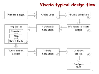
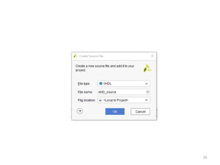
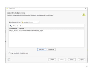
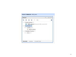
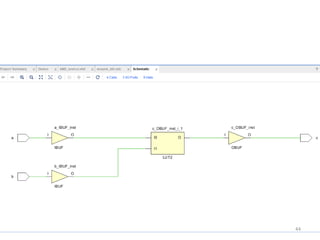
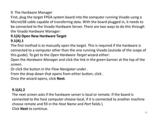
This document provides an overview of getting started with Vivado, Xilinx's IDE for FPGA design and implementation. It describes how to create a Vivado project targeting a Nexys4 DDR board, add VHDL source files to implement a simple 2-input logic AND gate, add a user constraints file to map design pins to board pins, run synthesis, implementation and bitstream generation to create a programming file, and use the hardware manager to download the bitstream and verify the design functionality on the board. The objectives are to create a Vivado project from HDL sources targeting a specific FPGA, constrain pin locations, synthesize, implement and generate a bitstream to program the FPGA.