The document discusses MOSFETs, including:
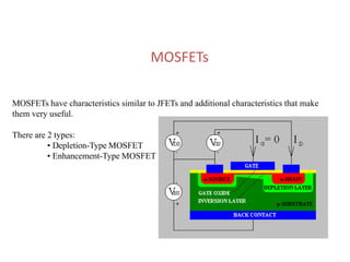
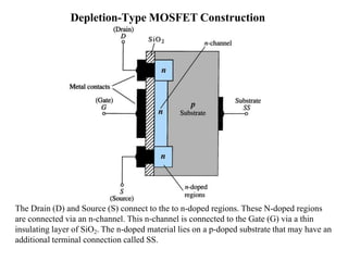
- There are two types of MOSFETs: depletion-type and enhancement-type.
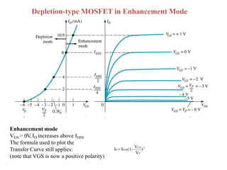
- Depletion-type MOSFETs can operate in depletion or enhancement mode depending on the gate-source voltage.
- Enhancement-type MOSFETs only operate in enhancement mode, where increasing the positive gate-source voltage above the threshold voltage increases drain current.
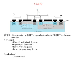
- CMOS uses both p-channel and n-channel enhancement-type MOSFETs on the same substrate, allowing for logic functions with high input impedance and low power.