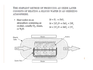
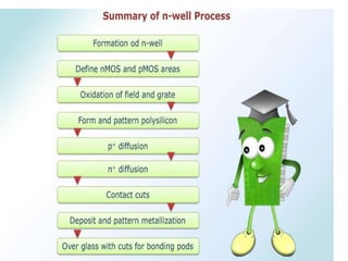
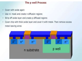
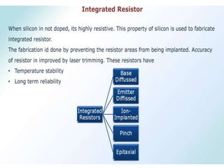
SlideShare a Scribd company logo
1 of 104
Tips for doing well in VLSI DESIGN
 Attend classes regularly, 75% attendance is mandatory
Work on your own for HW and Lab assignments
 Remember the study-lecture ratio
Study hrs. = Lecture hrs. x 3
Don’t just study for the exams - study to learn
 Study from text book and lecture notes thoroughly.
Don’t be afraid to ask questions
 As far as possible, study in groups – it helps a lot.
 If you want - we could arrange review sessions before exams.
But let me know in advance.
Don’t attempt to cheat !
- It’s you who will suffer in the exams.
Front End Design :
The front end design consists of those steps which involves manufacturing only on
softwares and functionality verification. It consists of following steps :
Design Specification : According to the requirements, they describe abstractly the
architecture, functionality and interface of the digital IC circuit to be designed. The
object is to describe the purpose of the design including all aspects, such as the
functions to be realized, timing constraints, and power dissipation requirements
etc.
Behavioural Description : Behavioral description is then created to analyze the
design in terms of functionality, performance, compliance to given standards, and
other specifications.
RTL Description : RTL description is done using HDLs and simulated to test
functionality. We need the help of EDA tools from here onwards. The various sub-
steps include verification of functionality and testing on a software. At the end, the
design is synthesized using the EDA tools and various timing constraints are
checked.
Back End Design :Back-end design, also known as physical design, involves the
translation of the RTL design into a physical layout that can be fabricated onto a chip.
Gate – level Netlist : RTL description is then converted to a gate-level netlist using
logic synthesis tools. It is a description of the circuit in terms of gates and connections
between them, such that they meet the timing, power and area specifications. The
design is partitioned into convenient compartments or functional blocks, placed on a
silicon floor and various interconnects are routed on the chip.
Physical Layout : Finally a physical layout is made, which will be verified and then
sent to fabrication.
Besides these three important parameters are to be kept in mind while designing the
VLSI circuits-Power, timing and area . According to the specifications, one parameter
is trade off above other. In order to tackle all these factor we have to consider as first
priority what the consumer want if someone want more speed then he/she has to
compromise with the power, and may be area it depends on architecture Overall,
Power consumption and area should be minimized and timing should be as fast as
possible.
The VLSI Design flow is a most general one. However different and efficient
methodology is being found out to have an efficient manufacturing of VLSI circuits
which are an unavoidable part of any electronic component. Obviously we want a
more fast and swift system which should be implemented on a small chip area and
having a consumption of very low power.
• Functional simulation is an iterative process, which
may require multiple simulations to achieve the
desired end functionality of the design.
• Synthesis is the process of transforming your HDL
design into a gate-level netlist, given all the specified
constraints and optimization settings i.e Hardware
SEMICONDUCTORS AND DOPING
 Adding trace amounts of certain materials to semiconductors alters
the crystal structure and can change their electrical properties in
particular it can change the number of free electrons or holes
 N-Type semiconductor has free electrons
 dopant is (typically) phosphorus, arsenic, antimony
 P-Type semiconductor has free holes
 dopant is (typically) boron, indium, gallium
 Dopants are usually implanted into the semiconductor using
Implantation Technology, followed by thermal process to diffuse
the dopants
 pMOS are 2.5 time slower than nMOS due to electron and hole
mobilities
f
• Computer-integrated manufacturing (CIM) is the manufacturing
approach of using computers to control entire production process.
This integration allows individual processes to exchange
information with each part.
• Chemical mechanical polishing (CMP) is a semiconductor process
technology that has been used for integrated circuit (IC)
manufacturing for more than 20 years.
• CMP or planarization is a process of smoothing surfaces with the
combination of chemical and mechanical forces.
• All the devices on the wafer are made at the same time
• After the circuitry has been placed on the chip
– the chip is over glassed (with a passivation layer) to protect it
– only those areas which connect to the outside world will be left
uncovered (the pads)
• The wafer finally passes to a test station
– test probes send test signal patterns to the chip and monitor the
output of the chip
• A chip with no manufacturing defect is called a good chip. Fraction
(or percentage) of good chips produced in a manufacturing process
is called the yield. The yield of a process is the percentage of die
which pass this testing.
• The wafer is then scribed and separated up into the individual chips.
These are then packaged
• Chips are ‘binned’ according to their performance
Czochralski Process is a Technique in Making Single-Crystal
Silicon
 A Solid Seed Crystal is Rotated and Slowly Extracted from a
Pool of Molten Si
 Requires Careful Control to Give Crystals Desired Purity and
Dimensions
The Silicon Cylinder is Known as an Ingot
Typical Ingot is About 1 or 2 Meters in Length Can be Sliced
into Hundreds of Smaller Circular Pieces Called Wafers
 Each Wafer Yields Hundreds or Thousands of Integrated
Circuits
WAFER MANUFACTURING
• The Silicon Crystal is Sliced by Using a Diamond-Tipped Saw into Thin
Wafers
• Sorted by Thickness
• Damaged Wafers Removed During Lapping
• Etch Wafers in Chemical to Remove any Remaining Crystal Damage
• Polishing Smoothes Uneven Surface Left by Sawing Process
OXIDATION
• SiO2 growth is a key process step in manufacturing all
Si devices
– Thick (- 1<mm) oxides are used for field oxides
(isolate devices from one another )
-Thin gate oxides (-100 Å) control MOS devices –for field
oxides
• The stability and ease of formation of SiO2 was one of
the reasons that Si replaced Ge as the semiconductor of
choice.
Dry oxide - Pure dry oxygen is employed
Disadvantage
- Dry oxide grows very slowly.
Advantage
 Oxide layers are very uniform.
 Relatively few defects exist at the oxide-silicon interface (These
defects interfere with the proper operation of semiconductor
devices)
 It has especially low surface state charges and thus make ideal
dielectrics for MOS transistors.
Wet oxide - In the same way as dry oxides, but steam is
injected.
Disadvantage
- Hydrogen atoms liberated by the decomposition of the
water molecules produce imperfections that may
degrade the oxide quality.
Advantage
- Wet oxide grows fast.
- Useful to grow a thick layer of field oxide
COMPARISON OF DIFFUSION AND ION IMPLANTATION
Diffusion is a cheaper and more simplistic method, but can only be
performed from the surface of the wafers.
Dopants also diffuse unevenly, and interact with each other altering
the diffusion rate.
Ion implantation is more expensive and complex. It does not require
high temperatures and also allows for greater control of dopant
concentration and profile.
It is an anisotropic process and therefore does not spread the dopant
implant as much as diffusion. This aids in the manufacture of self-
aligned structures which greatly improve the performance of MOS
transistors.
TWIN TUB PROCESS
Integrated circuits are made of various electronic components, which are
assembled as per the micro architecture design, to form the final circuit. Some
typical circuit components in an IC are as follows
1. Resistors and conductors 2. Capacitors 3. Diodes 4. Transistors 5. Fuses
 Resistors are used for controlling the current flow. Every doped or undoped
region in a wafer is a resistor. Dopant concentration is used for controlling
the resistance.
 Resistors can be formed by isolating regions of the wafer by using suitable
dielectrics. For a region of length L and area A, the resistance is given by
R = ρLA
where ρ is the resistivity of Si .
 A doped resistor can be made by patterning and exposing a certain region on the
wafer, which is then doped to the desired concentration.
 Electrical contacts are provided by Ohmic contacts and the resistor region is
separated from the rest of the wafer by either silicon oxide or nitride.
Integrated resistors and capacitors
Resistors can be linear or serpentine.
Serpentine resistors are used for increasing resistance by
increasing total length.
Epi resistors are formed by isolating a section of an epitaxial Si
layer that has been deposited by chemical vapor deposition
process.
The resistor is isolated using trenches and the contacts are
patterned through the oxide layer on top.
Pinch resistors are formed by having alternately doped regions
(like a npn BJT). The base region between the junctions are the
pinch resistors,
P-layer Substrate Manufacture. Being the base
layer of the IC, the P-type is silicon is first built
for the IC. ...
N-type Epitaxial Growth. ...
The Silicon Dioxide Insulation Layer. ...
Photolithographic Process for SiO2. ...
Isolation Diffusion. ...
Base Diffusion. ...
Emitter Diffusion. ...
Aluminium Metallization.
 A capacitor is a dielectric region sandwiched between two electrodes. The
simplest dielectric structure is the metal oxide semiconductor (MOS)
structure.
 The contact can be a metal layer or heavily doped poly Si. These
structures are similar to those created for the MOSFETs, except for the
absence of the source and drain.
 The arrangement of the MOS capacitor is similar to a parallel plate
capacitor. The dielectric material can be silicon oxide or oxy-nitride or a
high-k dielectric material.
 Another technique to form capacitors, is to use the depletion region, which
is formed between p − n junction. The junction capacitance value is
important for circuit design since it affects the speed of the circuit. The
natural junction capacitance has the effect of slowing down the circuit.
 In order to save space, capacitors can also be fabricated perpendicular to
the wafer surface. These are called trench capacitors, Trench capacitors are
typically grown by CVD, since they are high aspect ratio structures. One
of the contacts is poly Si while oxide is the dielectric material.
UNIT-1 VLSID-MREC-ECE-Dr.TM.pptx

More Related Content

Similar to UNIT-1 VLSID-MREC-ECE-Dr.TM.pptx

18EC655_Module-1.pptx
18EC655_Module-1.pptx18EC655_Module-1.pptx
18EC655_Module-1.pptxJazzSameer
 
Introduction To Microelectronics
Introduction To MicroelectronicsIntroduction To Microelectronics
Introduction To MicroelectronicsAnkita Jaiswal
 
Flipchip bonding.
Flipchip bonding.Flipchip bonding.
Flipchip bonding.venkata016
 
Integrated Circuits
Integrated CircuitsIntegrated Circuits
Integrated CircuitsANAND G
 
Printed Circuit Board Design Techniques for EMC Compliance_20240220_145105_00...
Printed Circuit Board Design Techniques for EMC Compliance_20240220_145105_00...Printed Circuit Board Design Techniques for EMC Compliance_20240220_145105_00...
Printed Circuit Board Design Techniques for EMC Compliance_20240220_145105_00...AlanGustavo13
 
Printed circuit board
Printed circuit boardPrinted circuit board
Printed circuit boardSuhail Ahmed
 
Chapter 1-IC Fabrication.pptx
Chapter 1-IC Fabrication.pptxChapter 1-IC Fabrication.pptx
Chapter 1-IC Fabrication.pptxKarthik Prof.
 
Lecture 2 ic fabrication processing & wafer preparation
Lecture 2 ic fabrication processing & wafer preparationLecture 2 ic fabrication processing & wafer preparation
Lecture 2 ic fabrication processing & wafer preparationDr. Ghanshyam Singh
 
Making of an Application Specific Integrated Circuit
Making of an Application Specific Integrated CircuitMaking of an Application Specific Integrated Circuit
Making of an Application Specific Integrated CircuitSWINDONSilicon
 
Low power in vlsi with upf basics part 1
Low power in vlsi with upf basics part 1Low power in vlsi with upf basics part 1
Low power in vlsi with upf basics part 1SUNODH GARLAPATI
 
Advanced mosfet architectures
Advanced mosfet architecturesAdvanced mosfet architectures
Advanced mosfet architecturesDenita Tom
 
Monolithic implementation of parasitic elements
Monolithic implementation of parasitic elementsMonolithic implementation of parasitic elements
Monolithic implementation of parasitic elementsGOPICHAND NAGUBOINA
 

Similar to UNIT-1 VLSID-MREC-ECE-Dr.TM.pptx (20)

basic vlsi ppt
basic vlsi pptbasic vlsi ppt
basic vlsi ppt
 
18EC655_Module-1.pptx
18EC655_Module-1.pptx18EC655_Module-1.pptx
18EC655_Module-1.pptx
 
Introduction To Microelectronics
Introduction To MicroelectronicsIntroduction To Microelectronics
Introduction To Microelectronics
 
Ue 1(v sem)
Ue 1(v sem)Ue 1(v sem)
Ue 1(v sem)
 
VLSIM2.pptx
VLSIM2.pptxVLSIM2.pptx
VLSIM2.pptx
 
VLSI FUNDAMENTALS--ABU SYED KUET
VLSI FUNDAMENTALS--ABU SYED KUETVLSI FUNDAMENTALS--ABU SYED KUET
VLSI FUNDAMENTALS--ABU SYED KUET
 
Flipchip bonding.
Flipchip bonding.Flipchip bonding.
Flipchip bonding.
 
Beyond cmos
Beyond cmosBeyond cmos
Beyond cmos
 
Integrated Circuits
Integrated CircuitsIntegrated Circuits
Integrated Circuits
 
integratedcircuits
integratedcircuitsintegratedcircuits
integratedcircuits
 
My VLSI.pptx
My VLSI.pptxMy VLSI.pptx
My VLSI.pptx
 
Printed Circuit Board Design Techniques for EMC Compliance_20240220_145105_00...
Printed Circuit Board Design Techniques for EMC Compliance_20240220_145105_00...Printed Circuit Board Design Techniques for EMC Compliance_20240220_145105_00...
Printed Circuit Board Design Techniques for EMC Compliance_20240220_145105_00...
 
Printed circuit board
Printed circuit boardPrinted circuit board
Printed circuit board
 
Chapter 1-IC Fabrication.pptx
Chapter 1-IC Fabrication.pptxChapter 1-IC Fabrication.pptx
Chapter 1-IC Fabrication.pptx
 
Lecture 2 ic fabrication processing & wafer preparation
Lecture 2 ic fabrication processing & wafer preparationLecture 2 ic fabrication processing & wafer preparation
Lecture 2 ic fabrication processing & wafer preparation
 
Making of an Application Specific Integrated Circuit
Making of an Application Specific Integrated CircuitMaking of an Application Specific Integrated Circuit
Making of an Application Specific Integrated Circuit
 
Low power in vlsi with upf basics part 1
Low power in vlsi with upf basics part 1Low power in vlsi with upf basics part 1
Low power in vlsi with upf basics part 1
 
Advanced mosfet architectures
Advanced mosfet architecturesAdvanced mosfet architectures
Advanced mosfet architectures
 
Analog vlsi
Analog vlsiAnalog vlsi
Analog vlsi
 
Monolithic implementation of parasitic elements
Monolithic implementation of parasitic elementsMonolithic implementation of parasitic elements
Monolithic implementation of parasitic elements
 

More from 8885684828

vlsi-unit-3-ppt.pptx
vlsi-unit-3-ppt.pptxvlsi-unit-3-ppt.pptx
vlsi-unit-3-ppt.pptx8885684828
 
mosfet ppt.pptx
mosfet ppt.pptxmosfet ppt.pptx
mosfet ppt.pptx8885684828
 
denoising.pptx
denoising.pptxdenoising.pptx
denoising.pptx8885684828
 
verilog basics.ppt
verilog basics.pptverilog basics.ppt
verilog basics.ppt8885684828
 
Basic VLSI.ppt
Basic VLSI.pptBasic VLSI.ppt
Basic VLSI.ppt8885684828
 
literature.pptx
literature.pptxliterature.pptx
literature.pptx8885684828
 
water verflow.pdf
water verflow.pdfwater verflow.pdf
water verflow.pdf8885684828
 
PROJECT PPT (1).pptx
PROJECT PPT (1).pptxPROJECT PPT (1).pptx
PROJECT PPT (1).pptx8885684828
 

More from 8885684828 (12)

ASCIC.ppt
ASCIC.pptASCIC.ppt
ASCIC.ppt
 
Module-4.pdf
Module-4.pdfModule-4.pdf
Module-4.pdf
 
vlsi-unit-3-ppt.pptx
vlsi-unit-3-ppt.pptxvlsi-unit-3-ppt.pptx
vlsi-unit-3-ppt.pptx
 
mosfet ppt.pptx
mosfet ppt.pptxmosfet ppt.pptx
mosfet ppt.pptx
 
denoising.pptx
denoising.pptxdenoising.pptx
denoising.pptx
 
verilog basics.ppt
verilog basics.pptverilog basics.ppt
verilog basics.ppt
 
Basic VLSI.ppt
Basic VLSI.pptBasic VLSI.ppt
Basic VLSI.ppt
 
literature.pptx
literature.pptxliterature.pptx
literature.pptx
 
Module-5A.pdf
Module-5A.pdfModule-5A.pdf
Module-5A.pdf
 
LPVLSI.ppt
LPVLSI.pptLPVLSI.ppt
LPVLSI.ppt
 
water verflow.pdf
water verflow.pdfwater verflow.pdf
water verflow.pdf
 
PROJECT PPT (1).pptx
PROJECT PPT (1).pptxPROJECT PPT (1).pptx
PROJECT PPT (1).pptx
 

Recently uploaded

IMPLICATIONS OF THE ABOVE HOLISTIC UNDERSTANDING OF HARMONY ON PROFESSIONAL E...
IMPLICATIONS OF THE ABOVE HOLISTIC UNDERSTANDING OF HARMONY ON PROFESSIONAL E...IMPLICATIONS OF THE ABOVE HOLISTIC UNDERSTANDING OF HARMONY ON PROFESSIONAL E...
IMPLICATIONS OF THE ABOVE HOLISTIC UNDERSTANDING OF HARMONY ON PROFESSIONAL E...RajaP95
 
OSVC_Meta-Data based Simulation Automation to overcome Verification Challenge...
OSVC_Meta-Data based Simulation Automation to overcome Verification Challenge...OSVC_Meta-Data based Simulation Automation to overcome Verification Challenge...
OSVC_Meta-Data based Simulation Automation to overcome Verification Challenge...Soham Mondal
 
Porous Ceramics seminar and technical writing
Porous Ceramics seminar and technical writingPorous Ceramics seminar and technical writing
Porous Ceramics seminar and technical writingrakeshbaidya232001
 
Call Girls in Nagpur Suman Call 7001035870 Meet With Nagpur Escorts
Call Girls in Nagpur Suman Call 7001035870 Meet With Nagpur EscortsCall Girls in Nagpur Suman Call 7001035870 Meet With Nagpur Escorts
Call Girls in Nagpur Suman Call 7001035870 Meet With Nagpur EscortsCall Girls in Nagpur High Profile
 
Introduction to IEEE STANDARDS and its different types.pptx
Introduction to IEEE STANDARDS and its different types.pptxIntroduction to IEEE STANDARDS and its different types.pptx
Introduction to IEEE STANDARDS and its different types.pptxupamatechverse
 
Processing & Properties of Floor and Wall Tiles.pptx
Processing & Properties of Floor and Wall Tiles.pptxProcessing & Properties of Floor and Wall Tiles.pptx
Processing & Properties of Floor and Wall Tiles.pptxpranjaldaimarysona
 
Call for Papers - African Journal of Biological Sciences, E-ISSN: 2663-2187, ...
Call for Papers - African Journal of Biological Sciences, E-ISSN: 2663-2187, ...Call for Papers - African Journal of Biological Sciences, E-ISSN: 2663-2187, ...
Call for Papers - African Journal of Biological Sciences, E-ISSN: 2663-2187, ...Christo Ananth
 
Model Call Girl in Narela Delhi reach out to us at 🔝8264348440🔝
Model Call Girl in Narela Delhi reach out to us at 🔝8264348440🔝Model Call Girl in Narela Delhi reach out to us at 🔝8264348440🔝
Model Call Girl in Narela Delhi reach out to us at 🔝8264348440🔝soniya singh
 
College Call Girls Nashik Nehal 7001305949 Independent Escort Service Nashik
College Call Girls Nashik Nehal 7001305949 Independent Escort Service NashikCollege Call Girls Nashik Nehal 7001305949 Independent Escort Service Nashik
College Call Girls Nashik Nehal 7001305949 Independent Escort Service NashikCall Girls in Nagpur High Profile
 
UNIT-III FMM. DIMENSIONAL ANALYSIS
UNIT-III FMM.        DIMENSIONAL ANALYSISUNIT-III FMM.        DIMENSIONAL ANALYSIS
UNIT-III FMM. DIMENSIONAL ANALYSISrknatarajan
 
Introduction and different types of Ethernet.pptx
Introduction and different types of Ethernet.pptxIntroduction and different types of Ethernet.pptx
Introduction and different types of Ethernet.pptxupamatechverse
 
MANUFACTURING PROCESS-II UNIT-5 NC MACHINE TOOLS
MANUFACTURING PROCESS-II UNIT-5 NC MACHINE TOOLSMANUFACTURING PROCESS-II UNIT-5 NC MACHINE TOOLS
MANUFACTURING PROCESS-II UNIT-5 NC MACHINE TOOLSSIVASHANKAR N
 
Introduction to Multiple Access Protocol.pptx
Introduction to Multiple Access Protocol.pptxIntroduction to Multiple Access Protocol.pptx
Introduction to Multiple Access Protocol.pptxupamatechverse
 
(ANJALI) Dange Chowk Call Girls Just Call 7001035870 [ Cash on Delivery ] Pun...
(ANJALI) Dange Chowk Call Girls Just Call 7001035870 [ Cash on Delivery ] Pun...(ANJALI) Dange Chowk Call Girls Just Call 7001035870 [ Cash on Delivery ] Pun...
(ANJALI) Dange Chowk Call Girls Just Call 7001035870 [ Cash on Delivery ] Pun...ranjana rawat
 
(TARA) Talegaon Dabhade Call Girls Just Call 7001035870 [ Cash on Delivery ] ...
(TARA) Talegaon Dabhade Call Girls Just Call 7001035870 [ Cash on Delivery ] ...(TARA) Talegaon Dabhade Call Girls Just Call 7001035870 [ Cash on Delivery ] ...
(TARA) Talegaon Dabhade Call Girls Just Call 7001035870 [ Cash on Delivery ] ...ranjana rawat
 
(SHREYA) Chakan Call Girls Just Call 7001035870 [ Cash on Delivery ] Pune Esc...
(SHREYA) Chakan Call Girls Just Call 7001035870 [ Cash on Delivery ] Pune Esc...(SHREYA) Chakan Call Girls Just Call 7001035870 [ Cash on Delivery ] Pune Esc...
(SHREYA) Chakan Call Girls Just Call 7001035870 [ Cash on Delivery ] Pune Esc...ranjana rawat
 
(RIA) Call Girls Bhosari ( 7001035870 ) HI-Fi Pune Escorts Service
(RIA) Call Girls Bhosari ( 7001035870 ) HI-Fi Pune Escorts Service(RIA) Call Girls Bhosari ( 7001035870 ) HI-Fi Pune Escorts Service
(RIA) Call Girls Bhosari ( 7001035870 ) HI-Fi Pune Escorts Serviceranjana rawat
 

Recently uploaded (20)

IMPLICATIONS OF THE ABOVE HOLISTIC UNDERSTANDING OF HARMONY ON PROFESSIONAL E...
IMPLICATIONS OF THE ABOVE HOLISTIC UNDERSTANDING OF HARMONY ON PROFESSIONAL E...IMPLICATIONS OF THE ABOVE HOLISTIC UNDERSTANDING OF HARMONY ON PROFESSIONAL E...
IMPLICATIONS OF THE ABOVE HOLISTIC UNDERSTANDING OF HARMONY ON PROFESSIONAL E...
 
OSVC_Meta-Data based Simulation Automation to overcome Verification Challenge...
OSVC_Meta-Data based Simulation Automation to overcome Verification Challenge...OSVC_Meta-Data based Simulation Automation to overcome Verification Challenge...
OSVC_Meta-Data based Simulation Automation to overcome Verification Challenge...
 
Porous Ceramics seminar and technical writing
Porous Ceramics seminar and technical writingPorous Ceramics seminar and technical writing
Porous Ceramics seminar and technical writing
 
Call Girls in Nagpur Suman Call 7001035870 Meet With Nagpur Escorts
Call Girls in Nagpur Suman Call 7001035870 Meet With Nagpur EscortsCall Girls in Nagpur Suman Call 7001035870 Meet With Nagpur Escorts
Call Girls in Nagpur Suman Call 7001035870 Meet With Nagpur Escorts
 
Introduction to IEEE STANDARDS and its different types.pptx
Introduction to IEEE STANDARDS and its different types.pptxIntroduction to IEEE STANDARDS and its different types.pptx
Introduction to IEEE STANDARDS and its different types.pptx
 
Processing & Properties of Floor and Wall Tiles.pptx
Processing & Properties of Floor and Wall Tiles.pptxProcessing & Properties of Floor and Wall Tiles.pptx
Processing & Properties of Floor and Wall Tiles.pptx
 
Call for Papers - African Journal of Biological Sciences, E-ISSN: 2663-2187, ...
Call for Papers - African Journal of Biological Sciences, E-ISSN: 2663-2187, ...Call for Papers - African Journal of Biological Sciences, E-ISSN: 2663-2187, ...
Call for Papers - African Journal of Biological Sciences, E-ISSN: 2663-2187, ...
 
Call Us -/9953056974- Call Girls In Vikaspuri-/- Delhi NCR
Call Us -/9953056974- Call Girls In Vikaspuri-/- Delhi NCRCall Us -/9953056974- Call Girls In Vikaspuri-/- Delhi NCR
Call Us -/9953056974- Call Girls In Vikaspuri-/- Delhi NCR
 
Model Call Girl in Narela Delhi reach out to us at 🔝8264348440🔝
Model Call Girl in Narela Delhi reach out to us at 🔝8264348440🔝Model Call Girl in Narela Delhi reach out to us at 🔝8264348440🔝
Model Call Girl in Narela Delhi reach out to us at 🔝8264348440🔝
 
College Call Girls Nashik Nehal 7001305949 Independent Escort Service Nashik
College Call Girls Nashik Nehal 7001305949 Independent Escort Service NashikCollege Call Girls Nashik Nehal 7001305949 Independent Escort Service Nashik
College Call Girls Nashik Nehal 7001305949 Independent Escort Service Nashik
 
UNIT-III FMM. DIMENSIONAL ANALYSIS
UNIT-III FMM.        DIMENSIONAL ANALYSISUNIT-III FMM.        DIMENSIONAL ANALYSIS
UNIT-III FMM. DIMENSIONAL ANALYSIS
 
Introduction and different types of Ethernet.pptx
Introduction and different types of Ethernet.pptxIntroduction and different types of Ethernet.pptx
Introduction and different types of Ethernet.pptx
 
MANUFACTURING PROCESS-II UNIT-5 NC MACHINE TOOLS
MANUFACTURING PROCESS-II UNIT-5 NC MACHINE TOOLSMANUFACTURING PROCESS-II UNIT-5 NC MACHINE TOOLS
MANUFACTURING PROCESS-II UNIT-5 NC MACHINE TOOLS
 
Introduction to Multiple Access Protocol.pptx
Introduction to Multiple Access Protocol.pptxIntroduction to Multiple Access Protocol.pptx
Introduction to Multiple Access Protocol.pptx
 
9953056974 Call Girls In South Ex, Escorts (Delhi) NCR.pdf
9953056974 Call Girls In South Ex, Escorts (Delhi) NCR.pdf9953056974 Call Girls In South Ex, Escorts (Delhi) NCR.pdf
9953056974 Call Girls In South Ex, Escorts (Delhi) NCR.pdf
 
(ANJALI) Dange Chowk Call Girls Just Call 7001035870 [ Cash on Delivery ] Pun...
(ANJALI) Dange Chowk Call Girls Just Call 7001035870 [ Cash on Delivery ] Pun...(ANJALI) Dange Chowk Call Girls Just Call 7001035870 [ Cash on Delivery ] Pun...
(ANJALI) Dange Chowk Call Girls Just Call 7001035870 [ Cash on Delivery ] Pun...
 
(TARA) Talegaon Dabhade Call Girls Just Call 7001035870 [ Cash on Delivery ] ...
(TARA) Talegaon Dabhade Call Girls Just Call 7001035870 [ Cash on Delivery ] ...(TARA) Talegaon Dabhade Call Girls Just Call 7001035870 [ Cash on Delivery ] ...
(TARA) Talegaon Dabhade Call Girls Just Call 7001035870 [ Cash on Delivery ] ...
 
DJARUM4D - SLOT GACOR ONLINE | SLOT DEMO ONLINE
DJARUM4D - SLOT GACOR ONLINE | SLOT DEMO ONLINEDJARUM4D - SLOT GACOR ONLINE | SLOT DEMO ONLINE
DJARUM4D - SLOT GACOR ONLINE | SLOT DEMO ONLINE
 
(SHREYA) Chakan Call Girls Just Call 7001035870 [ Cash on Delivery ] Pune Esc...
(SHREYA) Chakan Call Girls Just Call 7001035870 [ Cash on Delivery ] Pune Esc...(SHREYA) Chakan Call Girls Just Call 7001035870 [ Cash on Delivery ] Pune Esc...
(SHREYA) Chakan Call Girls Just Call 7001035870 [ Cash on Delivery ] Pune Esc...
 
(RIA) Call Girls Bhosari ( 7001035870 ) HI-Fi Pune Escorts Service
(RIA) Call Girls Bhosari ( 7001035870 ) HI-Fi Pune Escorts Service(RIA) Call Girls Bhosari ( 7001035870 ) HI-Fi Pune Escorts Service
(RIA) Call Girls Bhosari ( 7001035870 ) HI-Fi Pune Escorts Service
 

UNIT-1 VLSID-MREC-ECE-Dr.TM.pptx

  • 1. Tips for doing well in VLSI DESIGN  Attend classes regularly, 75% attendance is mandatory Work on your own for HW and Lab assignments  Remember the study-lecture ratio Study hrs. = Lecture hrs. x 3 Don’t just study for the exams - study to learn  Study from text book and lecture notes thoroughly. Don’t be afraid to ask questions  As far as possible, study in groups – it helps a lot.  If you want - we could arrange review sessions before exams. But let me know in advance.
  • 2. Don’t attempt to cheat ! - It’s you who will suffer in the exams.
  • 3.
  • 4. Front End Design : The front end design consists of those steps which involves manufacturing only on softwares and functionality verification. It consists of following steps : Design Specification : According to the requirements, they describe abstractly the architecture, functionality and interface of the digital IC circuit to be designed. The object is to describe the purpose of the design including all aspects, such as the functions to be realized, timing constraints, and power dissipation requirements etc. Behavioural Description : Behavioral description is then created to analyze the design in terms of functionality, performance, compliance to given standards, and other specifications. RTL Description : RTL description is done using HDLs and simulated to test functionality. We need the help of EDA tools from here onwards. The various sub- steps include verification of functionality and testing on a software. At the end, the design is synthesized using the EDA tools and various timing constraints are checked.
  • 5. Back End Design :Back-end design, also known as physical design, involves the translation of the RTL design into a physical layout that can be fabricated onto a chip. Gate – level Netlist : RTL description is then converted to a gate-level netlist using logic synthesis tools. It is a description of the circuit in terms of gates and connections between them, such that they meet the timing, power and area specifications. The design is partitioned into convenient compartments or functional blocks, placed on a silicon floor and various interconnects are routed on the chip. Physical Layout : Finally a physical layout is made, which will be verified and then sent to fabrication. Besides these three important parameters are to be kept in mind while designing the VLSI circuits-Power, timing and area . According to the specifications, one parameter is trade off above other. In order to tackle all these factor we have to consider as first priority what the consumer want if someone want more speed then he/she has to compromise with the power, and may be area it depends on architecture Overall, Power consumption and area should be minimized and timing should be as fast as possible. The VLSI Design flow is a most general one. However different and efficient methodology is being found out to have an efficient manufacturing of VLSI circuits which are an unavoidable part of any electronic component. Obviously we want a more fast and swift system which should be implemented on a small chip area and having a consumption of very low power.
  • 6. • Functional simulation is an iterative process, which may require multiple simulations to achieve the desired end functionality of the design. • Synthesis is the process of transforming your HDL design into a gate-level netlist, given all the specified constraints and optimization settings i.e Hardware
  • 7.
  • 8. SEMICONDUCTORS AND DOPING  Adding trace amounts of certain materials to semiconductors alters the crystal structure and can change their electrical properties in particular it can change the number of free electrons or holes  N-Type semiconductor has free electrons  dopant is (typically) phosphorus, arsenic, antimony  P-Type semiconductor has free holes  dopant is (typically) boron, indium, gallium  Dopants are usually implanted into the semiconductor using Implantation Technology, followed by thermal process to diffuse the dopants  pMOS are 2.5 time slower than nMOS due to electron and hole mobilities
  • 9.
  • 10.
  • 11.
  • 12.
  • 13.
  • 14.
  • 15. f
  • 16. • Computer-integrated manufacturing (CIM) is the manufacturing approach of using computers to control entire production process. This integration allows individual processes to exchange information with each part. • Chemical mechanical polishing (CMP) is a semiconductor process technology that has been used for integrated circuit (IC) manufacturing for more than 20 years. • CMP or planarization is a process of smoothing surfaces with the combination of chemical and mechanical forces.
  • 17. • All the devices on the wafer are made at the same time • After the circuitry has been placed on the chip – the chip is over glassed (with a passivation layer) to protect it – only those areas which connect to the outside world will be left uncovered (the pads) • The wafer finally passes to a test station – test probes send test signal patterns to the chip and monitor the output of the chip • A chip with no manufacturing defect is called a good chip. Fraction (or percentage) of good chips produced in a manufacturing process is called the yield. The yield of a process is the percentage of die which pass this testing. • The wafer is then scribed and separated up into the individual chips. These are then packaged • Chips are ‘binned’ according to their performance
  • 18.
  • 19.
  • 20.
  • 21.
  • 22.
  • 23.
  • 24.
  • 25.
  • 26.
  • 27. Czochralski Process is a Technique in Making Single-Crystal Silicon  A Solid Seed Crystal is Rotated and Slowly Extracted from a Pool of Molten Si  Requires Careful Control to Give Crystals Desired Purity and Dimensions The Silicon Cylinder is Known as an Ingot Typical Ingot is About 1 or 2 Meters in Length Can be Sliced into Hundreds of Smaller Circular Pieces Called Wafers  Each Wafer Yields Hundreds or Thousands of Integrated Circuits
  • 28.
  • 29. WAFER MANUFACTURING • The Silicon Crystal is Sliced by Using a Diamond-Tipped Saw into Thin Wafers • Sorted by Thickness • Damaged Wafers Removed During Lapping • Etch Wafers in Chemical to Remove any Remaining Crystal Damage • Polishing Smoothes Uneven Surface Left by Sawing Process
  • 30.
  • 31.
  • 32.
  • 33. OXIDATION • SiO2 growth is a key process step in manufacturing all Si devices – Thick (- 1<mm) oxides are used for field oxides (isolate devices from one another ) -Thin gate oxides (-100 Å) control MOS devices –for field oxides • The stability and ease of formation of SiO2 was one of the reasons that Si replaced Ge as the semiconductor of choice.
  • 34.
  • 35. Dry oxide - Pure dry oxygen is employed Disadvantage - Dry oxide grows very slowly. Advantage  Oxide layers are very uniform.  Relatively few defects exist at the oxide-silicon interface (These defects interfere with the proper operation of semiconductor devices)  It has especially low surface state charges and thus make ideal dielectrics for MOS transistors.
  • 36. Wet oxide - In the same way as dry oxides, but steam is injected. Disadvantage - Hydrogen atoms liberated by the decomposition of the water molecules produce imperfections that may degrade the oxide quality. Advantage - Wet oxide grows fast. - Useful to grow a thick layer of field oxide
  • 37.
  • 38.
  • 39.
  • 40.
  • 41.
  • 42.
  • 43.
  • 44.
  • 45.
  • 46.
  • 47.
  • 48.
  • 49.
  • 50.
  • 51.
  • 52.
  • 53.
  • 54.
  • 55.
  • 56.
  • 57. COMPARISON OF DIFFUSION AND ION IMPLANTATION Diffusion is a cheaper and more simplistic method, but can only be performed from the surface of the wafers. Dopants also diffuse unevenly, and interact with each other altering the diffusion rate. Ion implantation is more expensive and complex. It does not require high temperatures and also allows for greater control of dopant concentration and profile. It is an anisotropic process and therefore does not spread the dopant implant as much as diffusion. This aids in the manufacture of self- aligned structures which greatly improve the performance of MOS transistors.
  • 58.
  • 59.
  • 60.
  • 61.
  • 62.
  • 63.
  • 64.
  • 65.
  • 66.
  • 67.
  • 68.
  • 69.
  • 70.
  • 71.
  • 72.
  • 73.
  • 74.
  • 75.
  • 76.
  • 77.
  • 78.
  • 79.
  • 81.
  • 82.
  • 83. Integrated circuits are made of various electronic components, which are assembled as per the micro architecture design, to form the final circuit. Some typical circuit components in an IC are as follows 1. Resistors and conductors 2. Capacitors 3. Diodes 4. Transistors 5. Fuses  Resistors are used for controlling the current flow. Every doped or undoped region in a wafer is a resistor. Dopant concentration is used for controlling the resistance.  Resistors can be formed by isolating regions of the wafer by using suitable dielectrics. For a region of length L and area A, the resistance is given by R = ρLA where ρ is the resistivity of Si .  A doped resistor can be made by patterning and exposing a certain region on the wafer, which is then doped to the desired concentration.  Electrical contacts are provided by Ohmic contacts and the resistor region is separated from the rest of the wafer by either silicon oxide or nitride. Integrated resistors and capacitors
  • 84. Resistors can be linear or serpentine. Serpentine resistors are used for increasing resistance by increasing total length. Epi resistors are formed by isolating a section of an epitaxial Si layer that has been deposited by chemical vapor deposition process. The resistor is isolated using trenches and the contacts are patterned through the oxide layer on top. Pinch resistors are formed by having alternately doped regions (like a npn BJT). The base region between the junctions are the pinch resistors,
  • 85.
  • 86.
  • 87.
  • 88. P-layer Substrate Manufacture. Being the base layer of the IC, the P-type is silicon is first built for the IC. ... N-type Epitaxial Growth. ... The Silicon Dioxide Insulation Layer. ... Photolithographic Process for SiO2. ... Isolation Diffusion. ... Base Diffusion. ... Emitter Diffusion. ... Aluminium Metallization.
  • 89.
  • 90.
  • 91.  A capacitor is a dielectric region sandwiched between two electrodes. The simplest dielectric structure is the metal oxide semiconductor (MOS) structure.  The contact can be a metal layer or heavily doped poly Si. These structures are similar to those created for the MOSFETs, except for the absence of the source and drain.  The arrangement of the MOS capacitor is similar to a parallel plate capacitor. The dielectric material can be silicon oxide or oxy-nitride or a high-k dielectric material.  Another technique to form capacitors, is to use the depletion region, which is formed between p − n junction. The junction capacitance value is important for circuit design since it affects the speed of the circuit. The natural junction capacitance has the effect of slowing down the circuit.  In order to save space, capacitors can also be fabricated perpendicular to the wafer surface. These are called trench capacitors, Trench capacitors are typically grown by CVD, since they are high aspect ratio structures. One of the contacts is poly Si while oxide is the dielectric material.