#StandardsGoals for 2024: What’s new for BISAC - Tech Forum 2024
VLSI Design_ Stick Diagrams_slidess.pptx
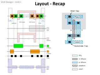
1. VLSI Design – Unit I
VLSI Design – Unit I
Layout - Recap
GND VDD
Y
A
substrate tap well tap
nMOS transistor pMOS transistor
Metal
Polysilicon
Contact
n+ Diffusion
p+ Diffusion
n well
2. VLSI Design – Unit I
VLSI Design – Unit I
Stick Diagram
Stick diagrams are used to display topography and layer information using simple
diagram – abstract model.
display layer information through colour coding.
If single colour is used, then line width and dashes are used to show different
layers.
An interface between symbolic circuit diagram and layout diagram.
show all components and via, and their relative placements.
need not to be of scale.
Stick diagrams do not show:
transistor sizes.
exact placement of components.
lengths, widths, well boundaries.
Metal 2
Metal 1
Metal 3
Poly-Si
N-diff
P-diff
Metal
Poly-Si
N-diff
P-diff
A stick diagram is a cartoon of a layout.
3. VLSI Design – Unit I
VLSI Design – Unit I
Stick Diagram Rules
Rule 1: When two or more sticks of same type (or layer) cross or touch each other,
there is an electrical contact between them.
Rule 2: When two or more sticks of different type cross or touch each other, there is
NO electrical contact between them.
If electrical contact is required, then show the connection explicitly.
4. VLSI Design – Unit I
VLSI Design – Unit I
Stick Diagram Rules (contd.)
Rule 3: When a poly cross the diffusion layer, then it represent a transistor.
If contact is shown, then it is not a transistor.
Rule 4: In CMOS a demarcation line is drawn to
avoid touching of p-diff with n-diff. All PMOS must lie
on one side of the line and all NMOS will have to be on
the other side.
pMOS at the top – pull-up network
nMOS at the bottom – pull-down network
5. VLSI Design – Unit I
VLSI Design – Unit I
How to draw Stick Diagram
First we’ll write the logic/Boolean expression in the complementary format.
Draw a static CMOS diagram.
Convert the design to stick diagram.
p-MOS
n-MOS
CMOS Inverter
VDD
A Y
GND
S
D
S
D
6. VLSI Design – Unit I
VLSI Design – Unit I
Euler Graph Technique can be used to determine if any complex CMOS gate can be
physically laid out in an optimum fashion!
Euler’s Path: path through all nodes in the graph such that each edge in the graph is
only visited once.
CMOS circuit equivalent:
Vertices – Source/Drain connections
Edges – Transistor gates that connect the S/D ‘Vertices’.
Diffusion – 1 row
PolySi runs vertically
Each transistor must “touch” electrically ones next to it – metal may be used.
To form an uninterrupted strip of diffusion, all transistors must be visited in sequence.
Both Euler paths for PUN and PDN must have the same sequence.
The sequence of edges in the Euler path equals the ordering of the inputs in the gate
layout.
Euler’s Path
Implement Boolean expression in the complementary format or CMOS Logic.
Draw a static CMOS diagram, and its logic graph.
Find a Euler path that cover the graph, sequence for PUN and PDN should be same.
Convert the design to stick diagram, keeping sequence of Euler path as the sequence
of the inputs.
7. VLSI Design – Unit I
VLSI Design – Unit I
Euler’s Path (Example)
A B C
8. VLSI Design – Unit I
VLSI Design – Unit I
Stick Diagram - Examples
CMOS NAND
A
B
Y
B A
VDD
GND
Vout
D D
S S
Y
D D
S S
A B
GND
VDD
(topological placement)
9. VLSI Design – Unit I
VLSI Design – Unit I
A
B
Y
Stick Diagram - Examples
CMOS NOR
10. VLSI Design – Unit I
VLSI Design – Unit I
Stick Diagram - Examples
11. VLSI Design – Unit I
VLSI Design – Unit I
MOS Transistor Characteristics
So far, we have treated transistors as ideal switches
MOS transistor is majority-carrier device.
Current in the conducting channel is controlled by VG.
An ON transistor passes a finite amount of current
Depends on terminal voltages
Derive current-voltage (I-V) relationships
• Transit times, Charge, carrier mobility, gate capacitance, Electric
field, permittivity of gate dielectric.
Transistor gate, source, drain all have capacitance
I = C (DV/Dt) -> Dt = (C/I) DV
Capacitance and current determine speed
12. VLSI Design – Unit I
VLSI Design – Unit I
MOS Capacitor
Gate and body form MOS capacitor
Operating mods
a) Accumulation
b) Depletion
c) Inversion
Threshold Voltage
Doping level
Thickness of oxide
13. VLSI Design – Unit I
VLSI Design – Unit I
Terminal Voltages
Mode of operation depends on Vg, Vd, Vs
Vgs = Vg – Vs
Vgd = Vg – Vd
Vds = Vd – Vs = Vgs – Vgd
Source and drain are symmetric diffusion
terminals
By convention, source is terminal at
lower voltage
Hence Vds 0
nMOS body is grounded. First assume source is 0
too.
Vg
Vs
Vd
Vgd
Vgs
Vds
+
-
+
-
+
-
14. VLSI Design – Unit I
VLSI Design – Unit I
nMOS Operation
Three regions of operation
Cutoff
• No channel
• Ids ≈ 0
Linear
• Channel forms
• Current flows from d to s
• e- from s to d
• Ids increases with Vds
• Similar to linear resistor
Saturation
• Channel pinches off
• Ids independent of Vds
• We say current saturates
• Similar to current source
+
-
Vgs
> Vt
n+ n+
+
-
Vgd
= Vgs
+
-
Vgs
> Vt
n+ n+
+
-
Vgs
> Vgd
> Vt
Vds
= 0
0 < Vds
< Vgs
-Vt
p-type body
p-type body
b
g
s d
b
g
s d
Ids
+
-
Vgs
= 0
n+ n+
+
-
Vgd
p-type body
b
g
s d
+
-
Vgs
> Vt
n+ n+
+
-
Vgd
< Vt
Vds
> Vgs
-Vt
p-type body
b
g
s d Ids
15. VLSI Design – Unit I
VLSI Design – Unit I
Long Channel I-V Characteristic
In Linear region, Ids depends on
How much charge is in the channel?
How fast is the charge moving?
Ids = Qchannel/t
t= time for charge to transit the channel
Assumption:
Channel length is long enough to have minimal lateral electric field.
Long-channel, Ideal, First-order, Shockley model.
Current (OFF) = 0.
16. VLSI Design – Unit I
VLSI Design – Unit I
Channel Charge
MOS structure looks like parallel plate capacitor while operating in inversions
(Q = CV)
Gate – oxide – channel
Qchannel = Cg (Vgc – Vt)
Cg = eoxWL/tox = CoxWL; Cox = eox / tox
V = Vgc – Vt = (Vgs – Vds/2) – Vt
• On the left of channel, Vgs
• On the right of Channel, Vgd =Vgs – Vds
• Computing the Average: Vgc = (Vgs + (Vgs – Vds))/2 = Vgs – Vds/2
Qchannel = CoxWL*((Vgs-Vds/2)-Vt)
17. VLSI Design – Unit I
VLSI Design – Unit I
Carrier Velocity
Charge is carried by e-
Carrier velocity, v, proportional to lateral E-field
v = mE m called mobility
Electron mobility ~ 2-3 times higher than hole mobility
Typical me- ~ 500-700 cm2/V.s
Electrons are propelled by the lateral electric field between source
and drain
E = Vds/L
Time for carrier to cross channel:
t = L / v
18. VLSI Design – Unit I
VLSI Design – Unit I
nMOS I-V: Linear
Now we know
How much charge Qchannel is in the channel
How much time t each carrier takes to cross
channel
ox 2
2
ds
ds
gs t ds
ds
gs t ds
Q
I
t
W V
C V V V
L
V
V V V
m
Linear Region:
Vgs > Vt
Vds ~ relatively small
19. VLSI Design – Unit I
VLSI Design – Unit I
nMOS I-V: Saturation
Vgd < Vt, channel pinches off near drain
Vds = VGT = Vgs-Vt
Channel no longer inverted in the vicinity of drain
When Vds > Vdsat = Vgs – Vt
Vdsat: Drain Saturation Voltage
Now drain voltage no longer increases current
2
2
2
dsat
ds gs t dsat
gs t
V
I V V V
V V
20. VLSI Design – Unit I
VLSI Design – Unit I
Long Channel I-V (nMOS)
2
cutoff
linear
saturatio
0
2
2
n
gs t
ds
ds gs t ds ds dsat
gs t ds dsat
V V
V
I V V V V V
V V V V
Shockley 1st order transistor models
21. VLSI Design – Unit I
VLSI Design – Unit I
Example
Fabrication process is 0.6 µm.
• From AMI Semiconductor
• tox = 100 Å
• m = 350 cm2/V*s
• Vt = 0.7 V
Plot Ids vs. Vds
• Vgs = 0, 1, 2, 3, 4, 5
• Use W/L = 4/2 l
14
2
8
3.9 8.85 10
350 120 μA/V
100 10
ox
W W W
C
L L L
m
0 1 2 3 4 5
0
0.5
1
1.5
2
2.5
Vds
I
ds
(mA)
Vgs
= 5
Vgs
= 4
Vgs
= 3
Vgs
= 2
Vgs
= 1
22. VLSI Design – Unit I
VLSI Design – Unit I
Capacitance
• Any two conductors separated by an insulator
have capacitance
• Gate to channel capacitor is very important
• Creates channel charge necessary for operation
• Source and drain have capacitance to body
• Across reverse-biased diodes
• Called diffusion capacitance because it is associated
with source/drain diffusion
23. VLSI Design – Unit I
VLSI Design – Unit I
Gate Capacitance
• Approximate channel as connected to
source
• Cgs = eoxWL/tox = CoxWL = CpermicronW
• Cpermicron is typically about 2 fF/mm
n+ n+
p-type body
W
L
tox
SiO2
gate oxide
(good insulator, eox
= 3.9e0
)
polysilicon
gate
24. VLSI Design – Unit I
VLSI Design – Unit I
Diffusion Capacitance
• Csb, Cdb
• Undesirable, called parasitic capacitance
• Capacitance depends on area and perimeter
• Use small diffusion nodes
• Comparable to Cg
for contacted diff
• ½ Cg for uncontacted
• Varies with process
In VLSI Design, firstly the front end engineer would design a circuit and then the back end engineer implement that design in VLSI chip.
Drawing these layouts to exact dimensions is very time consuming, and complicated to understand at a glance. We would like to have a way that may not be of size, but easy to understand the design concept.
Because deposition goes in layers.
Complementary format – pull-up n/w is in series, pull-down n/w is in parallel.
We learnt how to draw the static CMOS diagram in last class.
Mark the Gate, Source and Drain for the nMOS and pMOS.
Note: Source is the terminal closer to the supply rail, Drain is the terminal closer to the Output.
Marking S/D – S (next to VDD) for pMOS, S (next to GND) for nMOS. Drain of both nMOS and pMOS are connected together to output.
Euler’s path in a graph is defined as the path through …(bullet)
Sequence – drain of one device is the source of the next one.
N-MOS: Draw a p/n-diffusion layer, then draw a poly layer. – there is no contact to show a transistor.
CMOS inverter – first draw the metal rails for GND and VDD.
Euler’s path makes connection making for complex logic designs convenient.
Draw the VDD and GND rails – metal – blue, keep some space in middle to draw the logic.
Next draw the P-diffusion layer (yellow) and N-diffusion layer (green).
Then, we need transistors and need to draw polysilicon layers – depending on the number of inputs,, we’ll draw that many polysilicon layers – one input, one unbroken polysilicon layer. - we can see we get 2 transistors – mark S and D on these transistors.
Lastly we need to connect the source and drain of the transistors – make sure to put a black dot or (visually better) a cross to show the connections.
As seen from this example, we need to correctly draw the CMOS diagram first, and then convert it to stick diagram.
Also, marking the source and drains will make it easier to draw the connections.
** Performance and power of a chip depends on the current and capacitance of the transistors & Wires. (Bullet-ideal s/w)
Majority carrier device: nMOS – carriers are electrons; I controlled by V applied to Gate.
We’ll study ideal IV characteristics
MOS stack – good capacitor; used in operation.
Pn junctions from Source/Drain to body – parasitic capacitances.
Delay – determined by the time required for the current to charge or discharge the circuit capacitance.
Let’s consider a MOS structure – no S/D.
Body is grounded – voltage applied to the gate.
VG is –ve – positively charged holes are attracted to the region beneath the gate – accumulation Mode.
Small +ve VG – some +ve charge on Gate – holes are repelled from beneath the gate – depletion
+VG>Vthreshold – more +ve charge on gate – holes further repelled – electrons attracted – inversion layer is formed.
Vthreshold – number of dopants, tOX
MOS stack is between S&D.
Mode of operation depends on Vg, Vd, Vs.
* Potential difference between D & S, Vds=0 ie Vgs = Vgd – no electric field to push current from drain to source.
* Small +ve V applied to Drain – Current flows from D->S.
0<Vgs < VT – S/D: Free Electrons, Body: Free hole; Source – grounded – pn-junction @S-Body, Body-D: RB – little or no I – Cut off. IMP: we say no current. But this small leakage current through OFF Transistors become significant when multiplied by millions or billions of transistors on a chip.
Vgs > VT – inversion region of electrons – channel connect S & D – conductive path – transistor ON. Number of carriers increase with gate voltage and also drain V – Linear Region, also called – Resistive, Triode, Nonsaturated/Unsaturated.
Vds is large: Vgd<VT – Channel is no longer inverted near drain – pinch-off. Conduction is still occurs due to drift of electrons because of +ve drain V. (e- injected into depletion – accelerated towards Drain) – Saturation – I depends only on Vg.
Note: Threshold V of nMOS, pMOS are not necessarily equal.
By convention, majority carriers flow from S->D.
Lateral E-field: field b/w S & D – assumption no longer valid in nanometer devices.
Transistor ON – Vgs>Vt, channel is formed, Electrons drift from S-> D based on the electric field. Current can be computed, if we know charge in the channel, moving rate
Plate 1- gate, dielectric – oxide, plate 2 – channel
Cg: Gate-channel Capacitance; Vgc: Gate-Channel Potential;
Cox: Capacitance per unit area of gate oxide.
Vgc-Vt: amount of Voltage attracting charge to the channel, after inversion layer has been formed (at Vt).
Note: Nanometer devices – higher-k dielectric (such as HfO2, TiO2, Al2O3) are used – For same C, thinner films – Equivalent Oxide Thickness
( In smaller dimensions, “constants vary and variables don’t.”
Even though mobility is a constant, that’s true only in lower E-fields. For today’s short channel transistors with far higher fields, mobility is reduced. )
Time = channel length/velocity