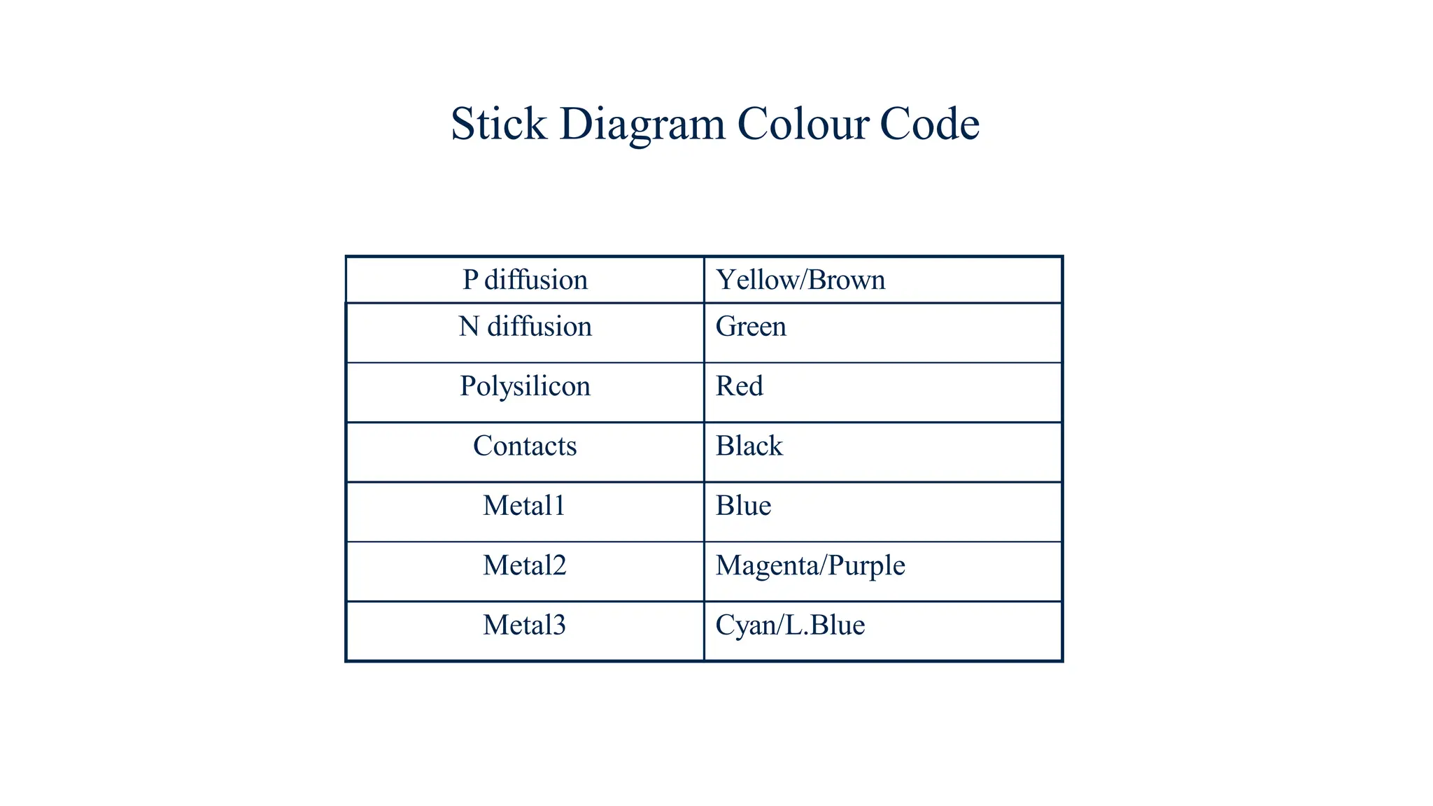
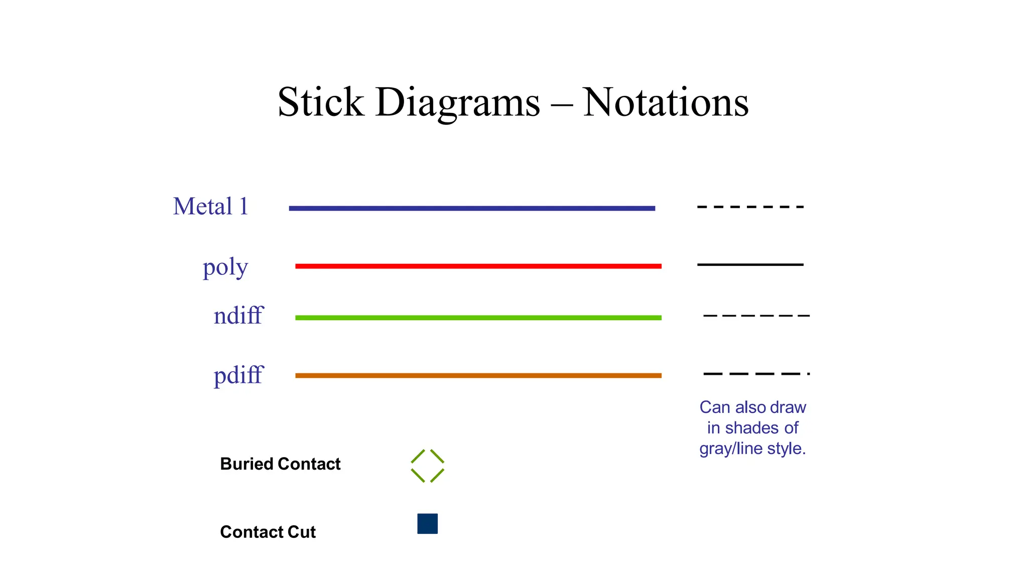
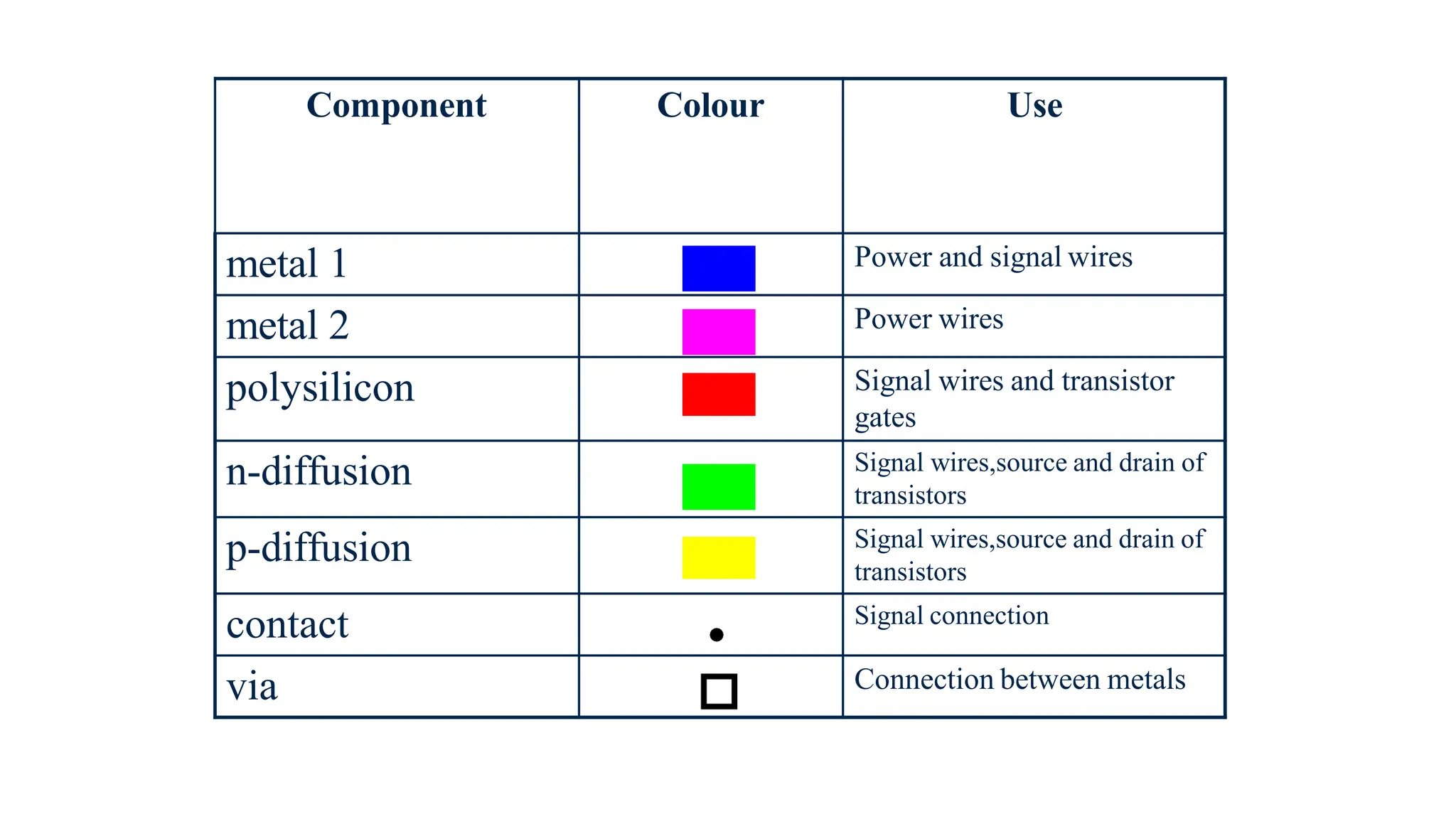
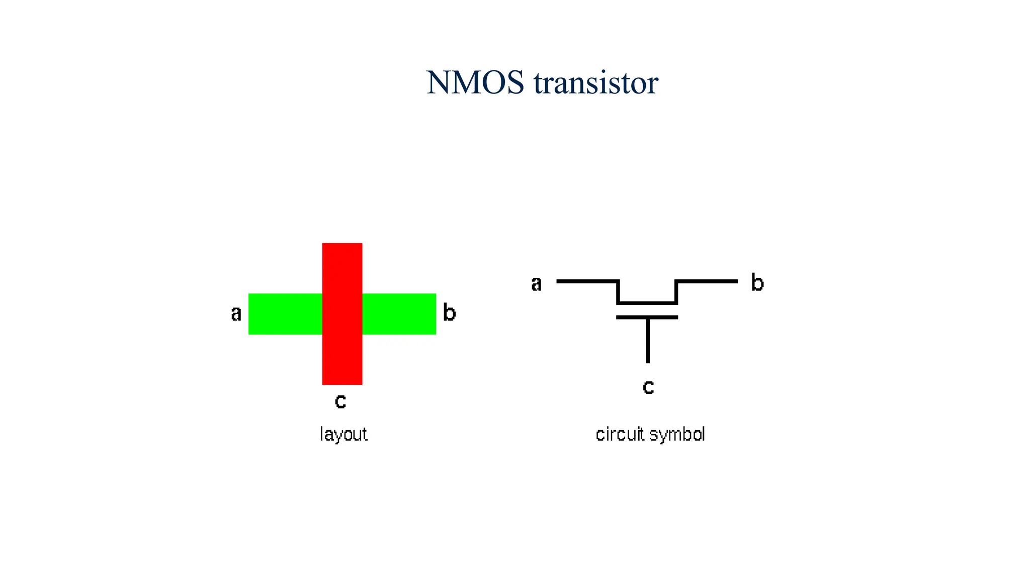
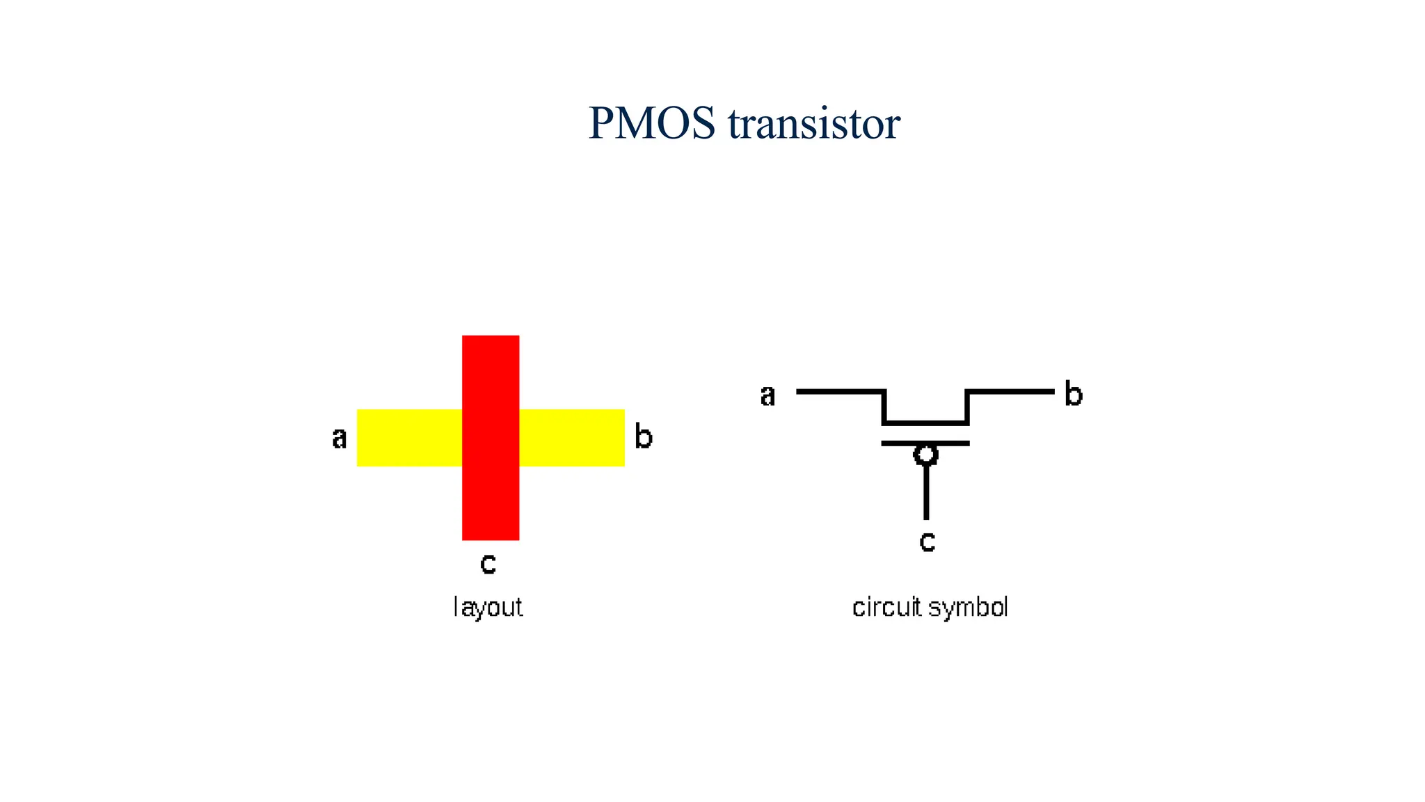
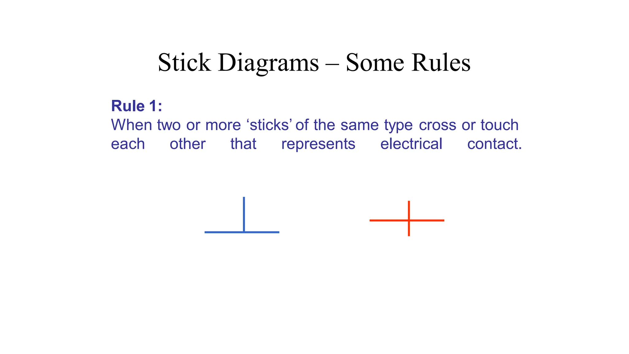
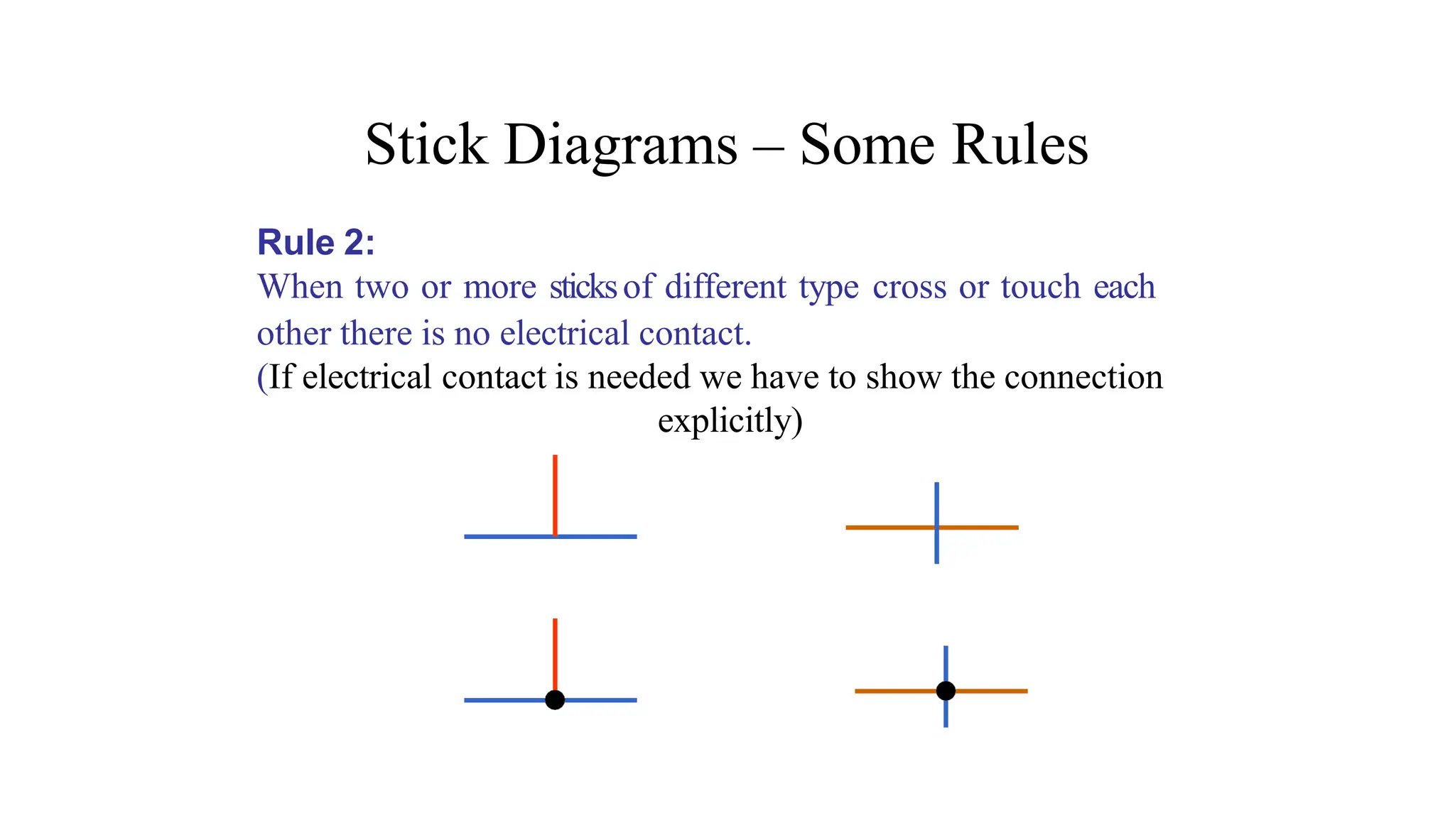
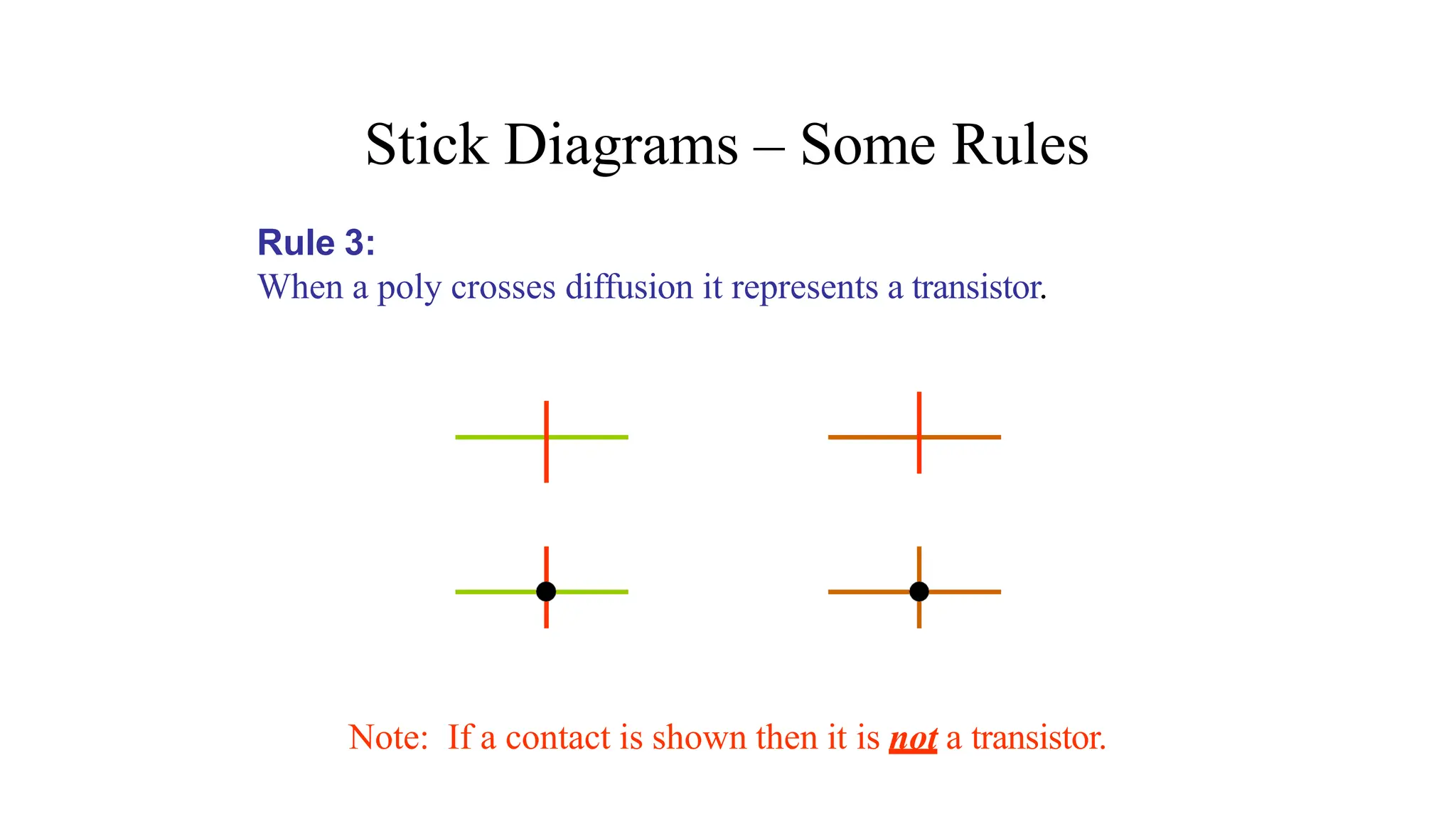
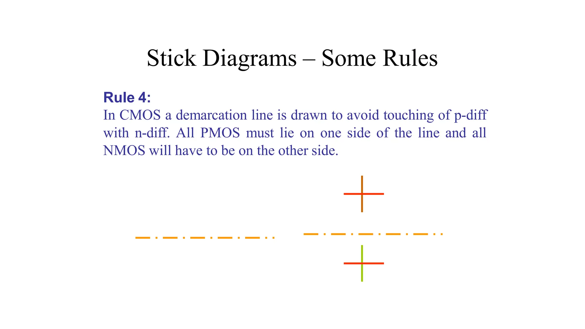
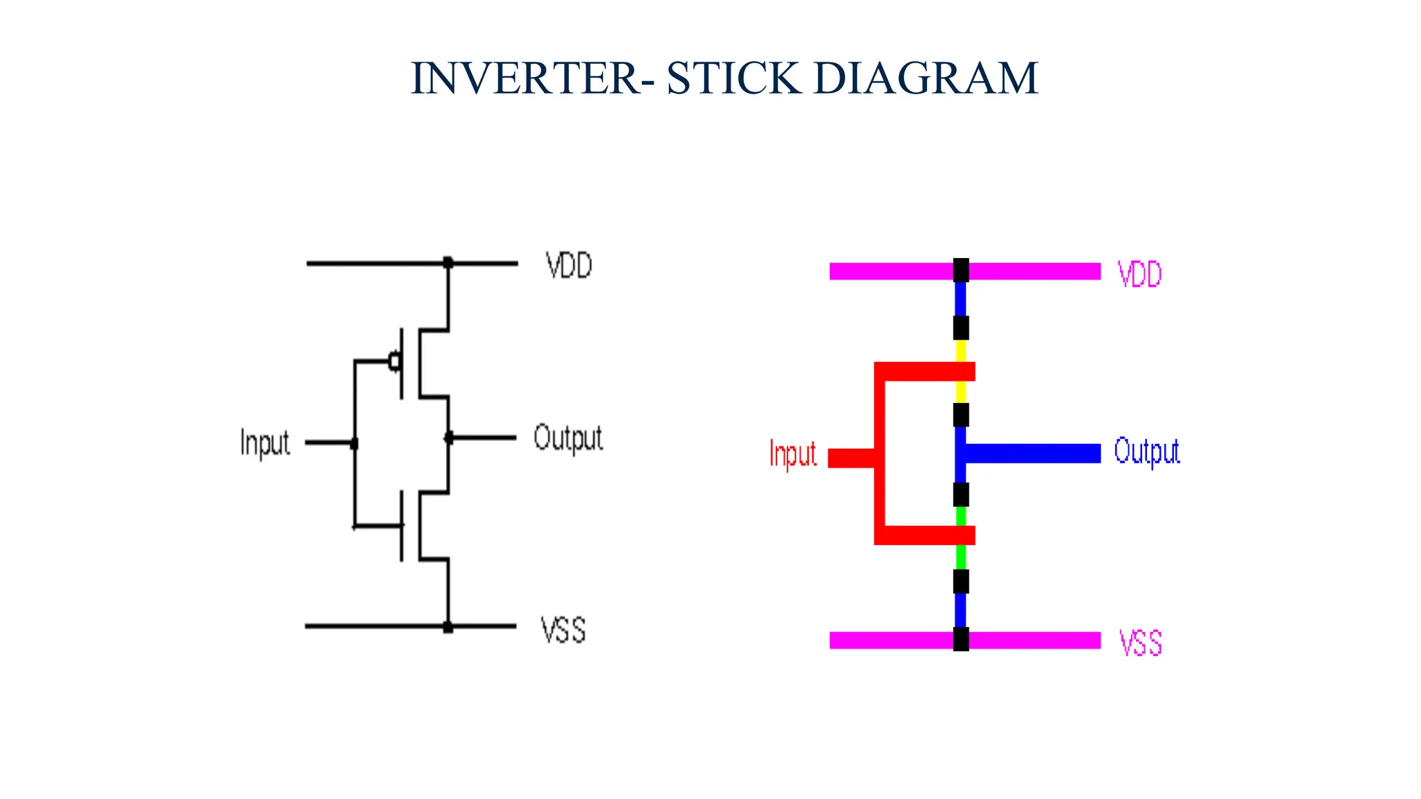
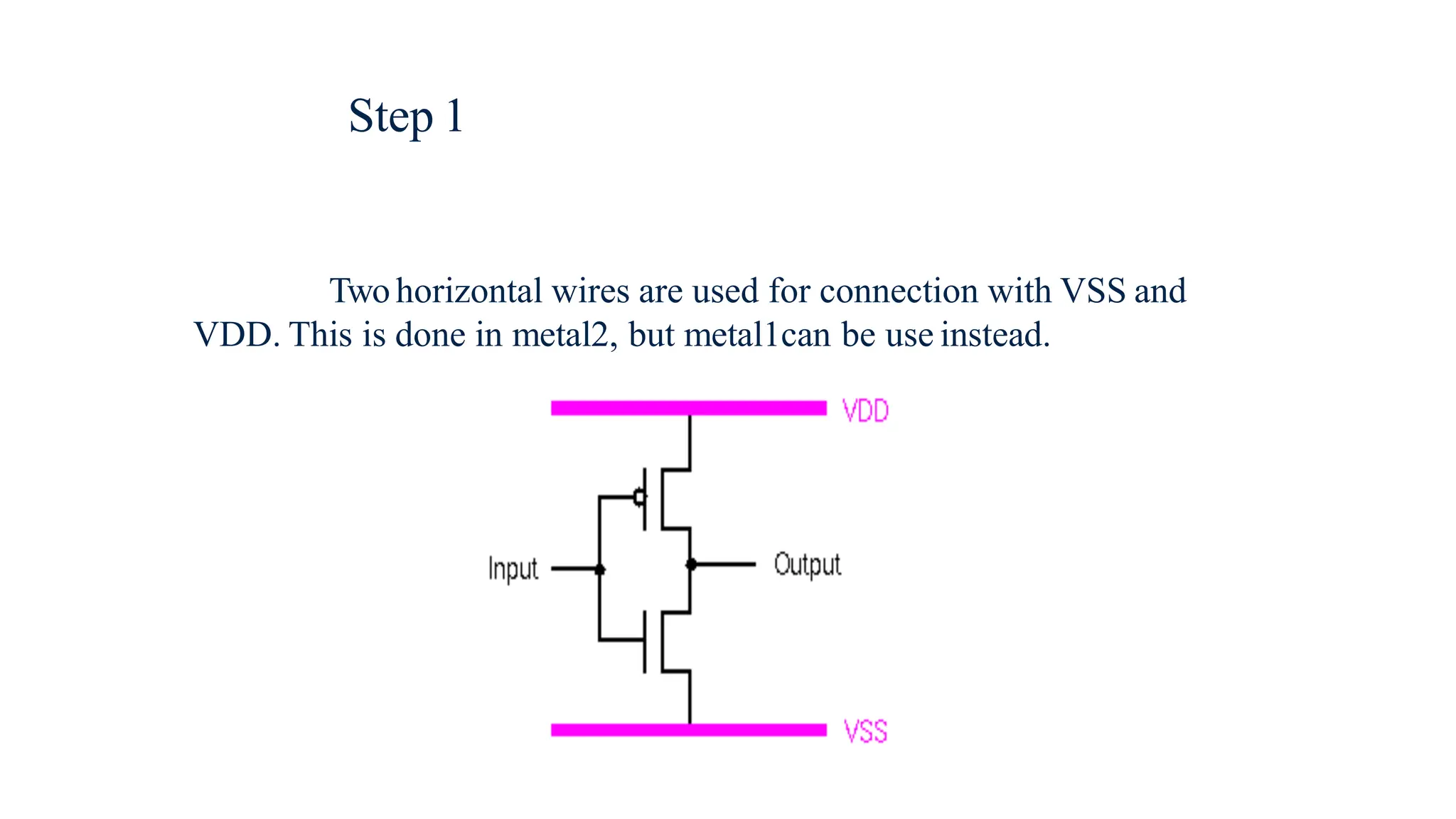
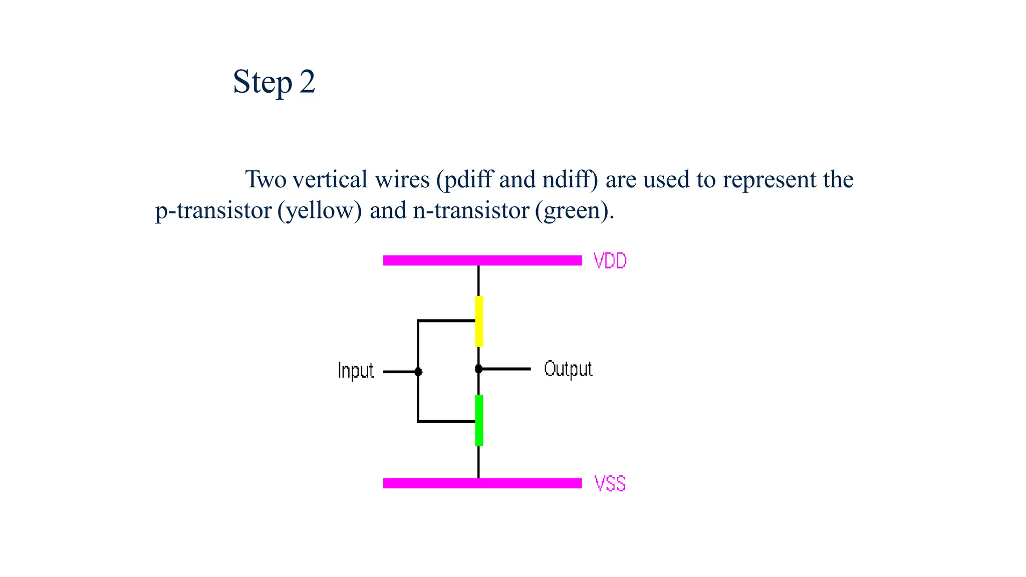
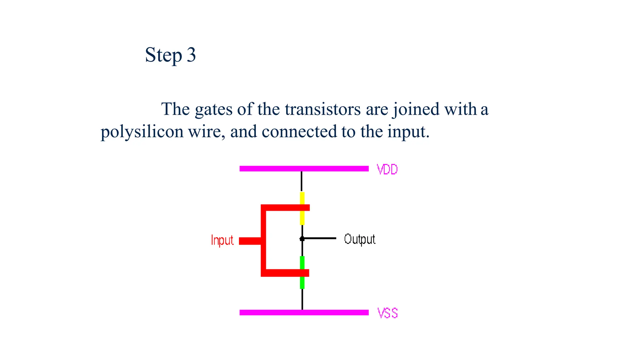
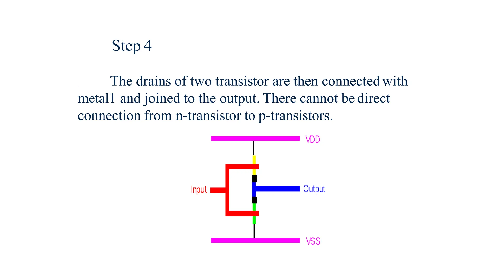
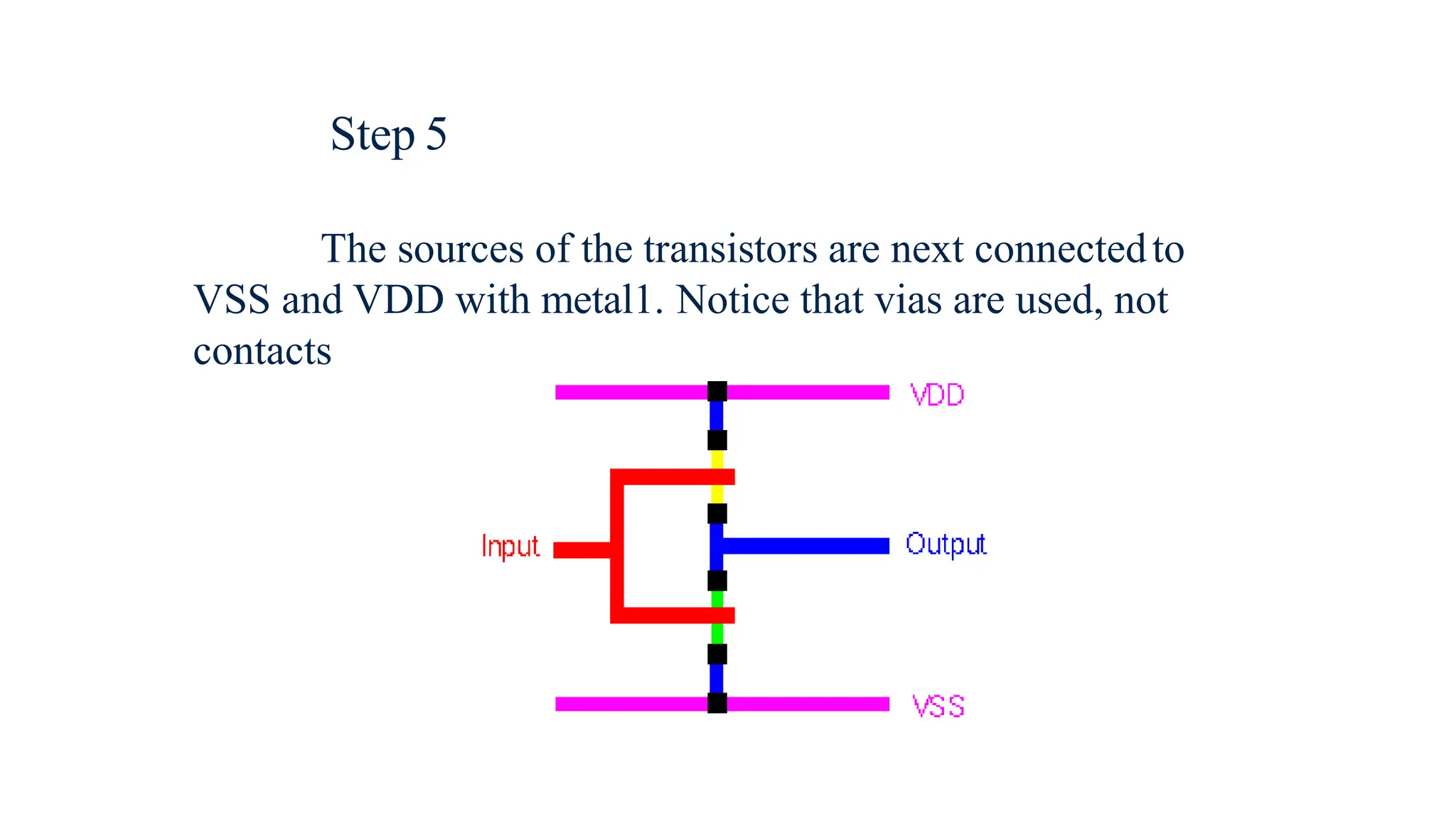
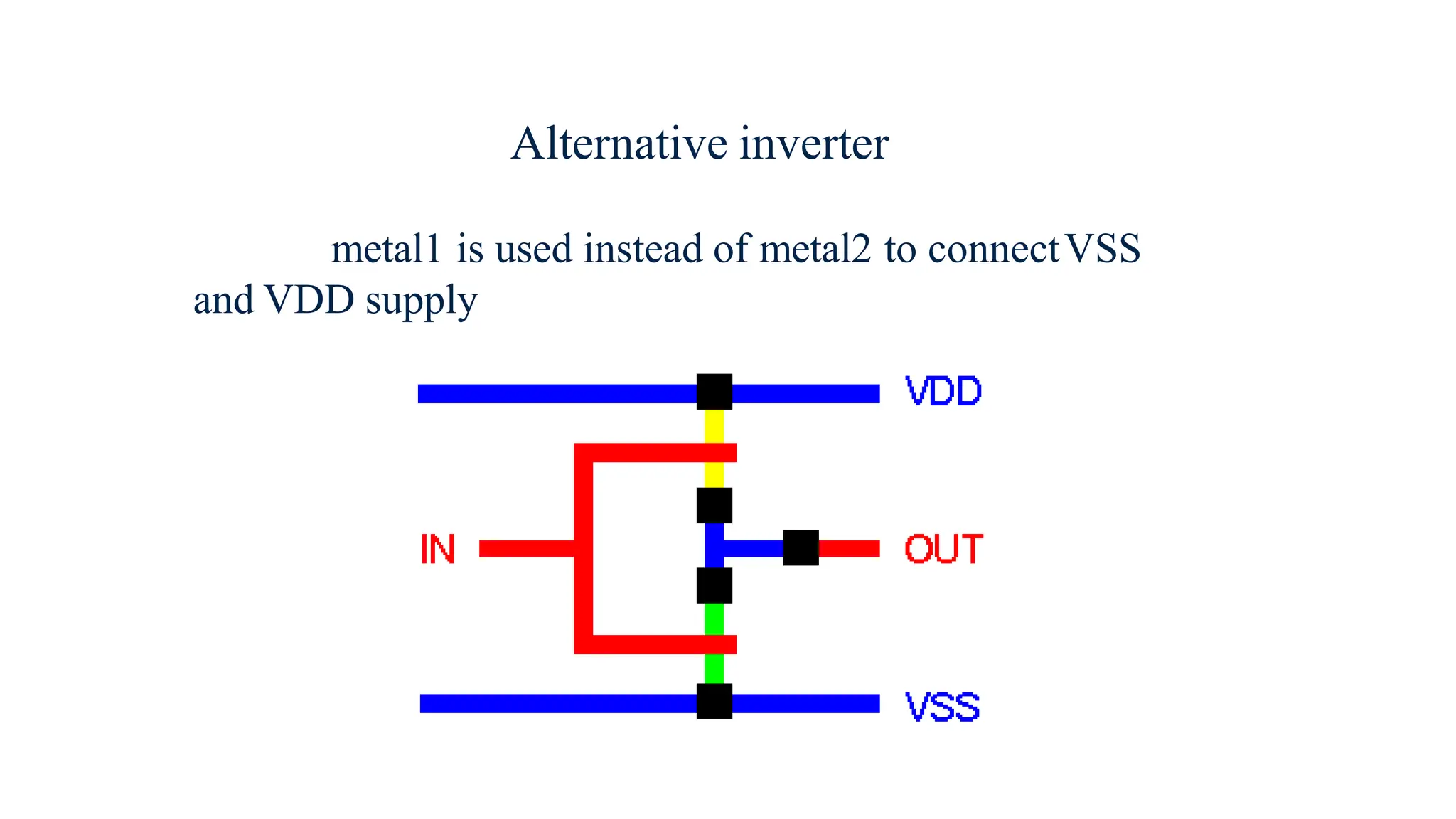
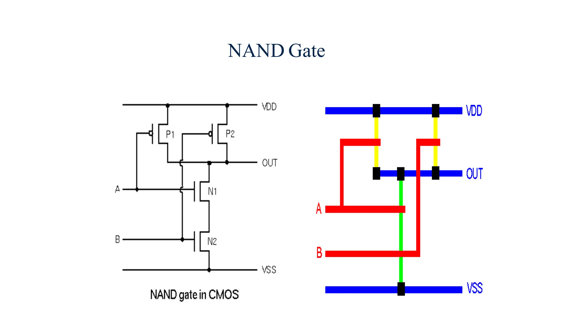
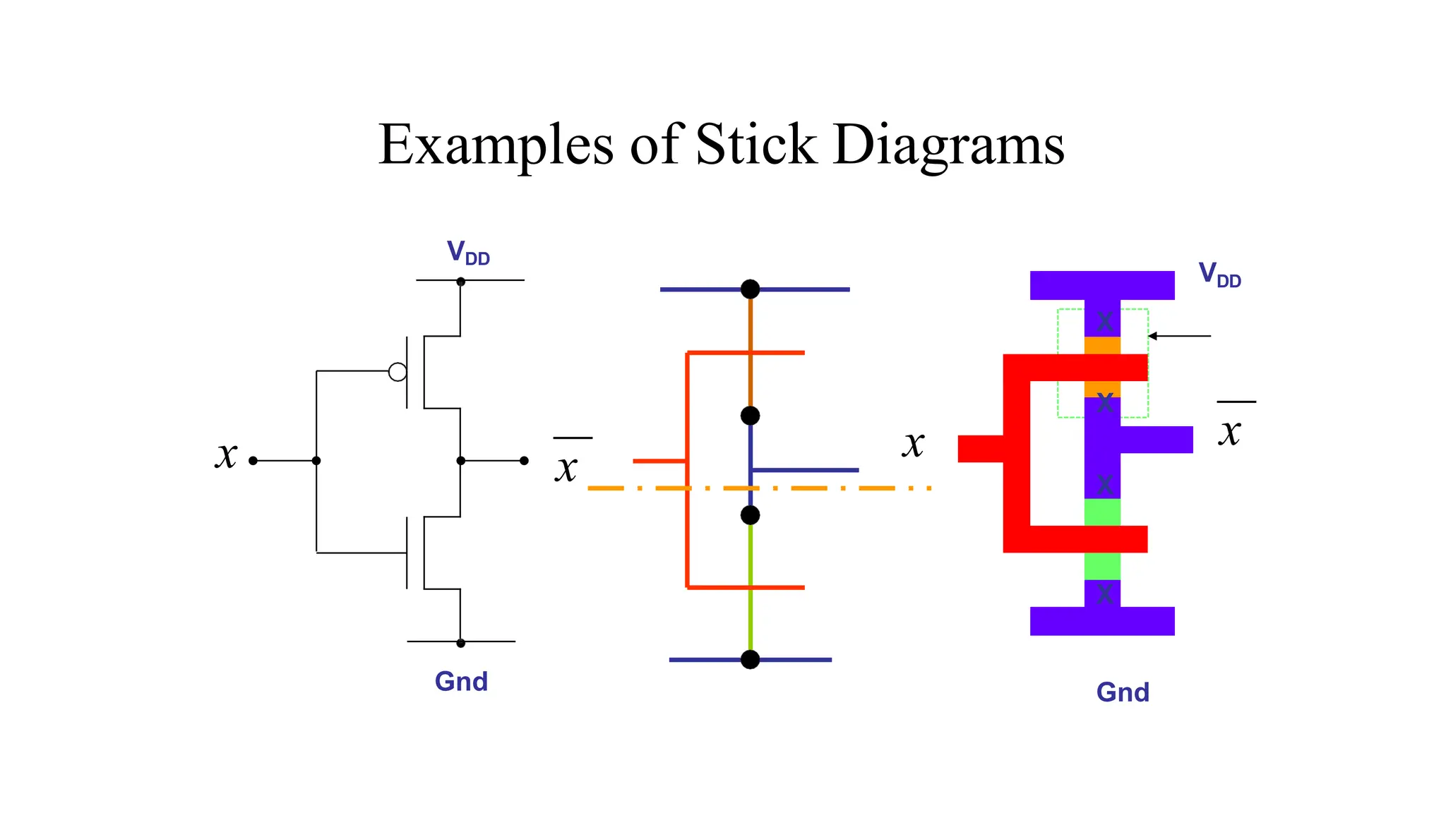
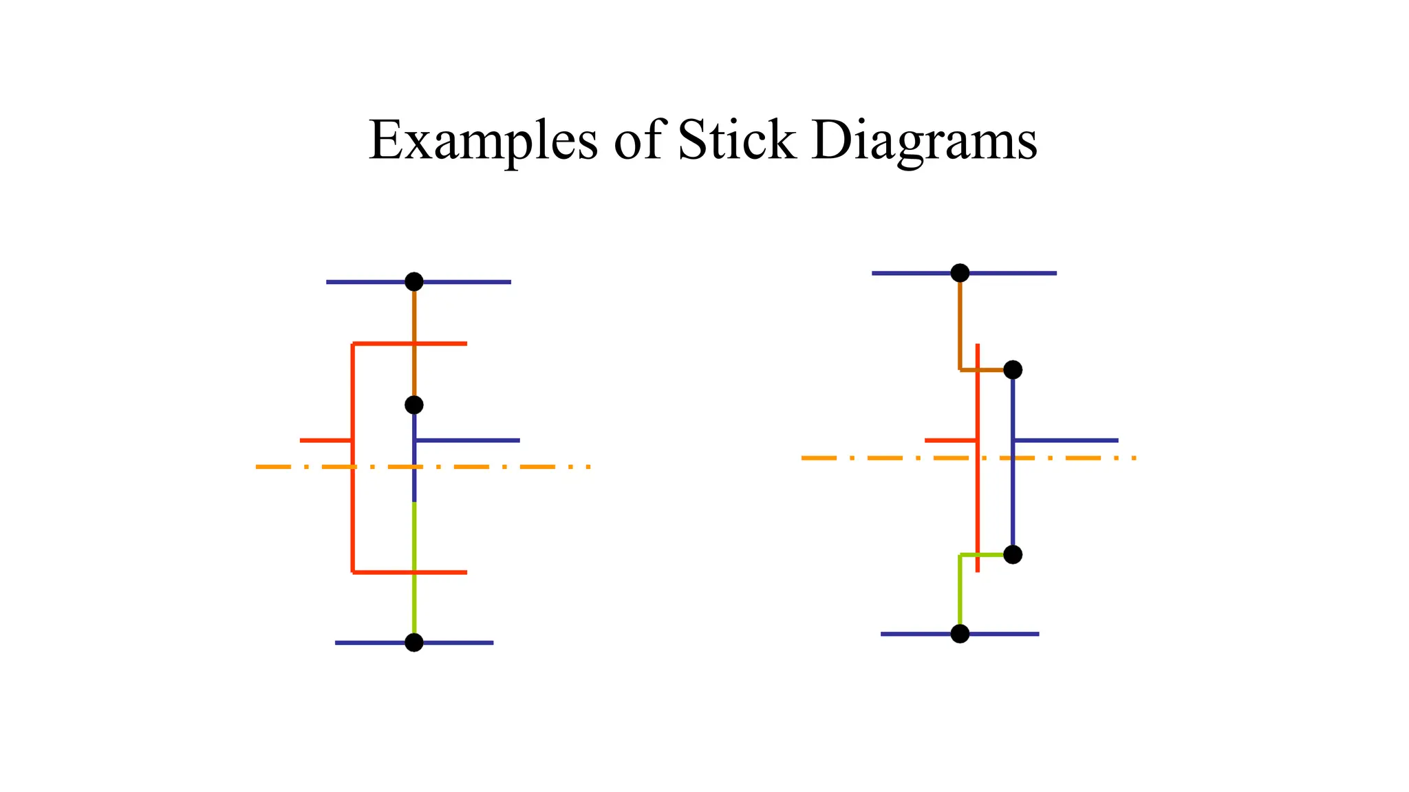
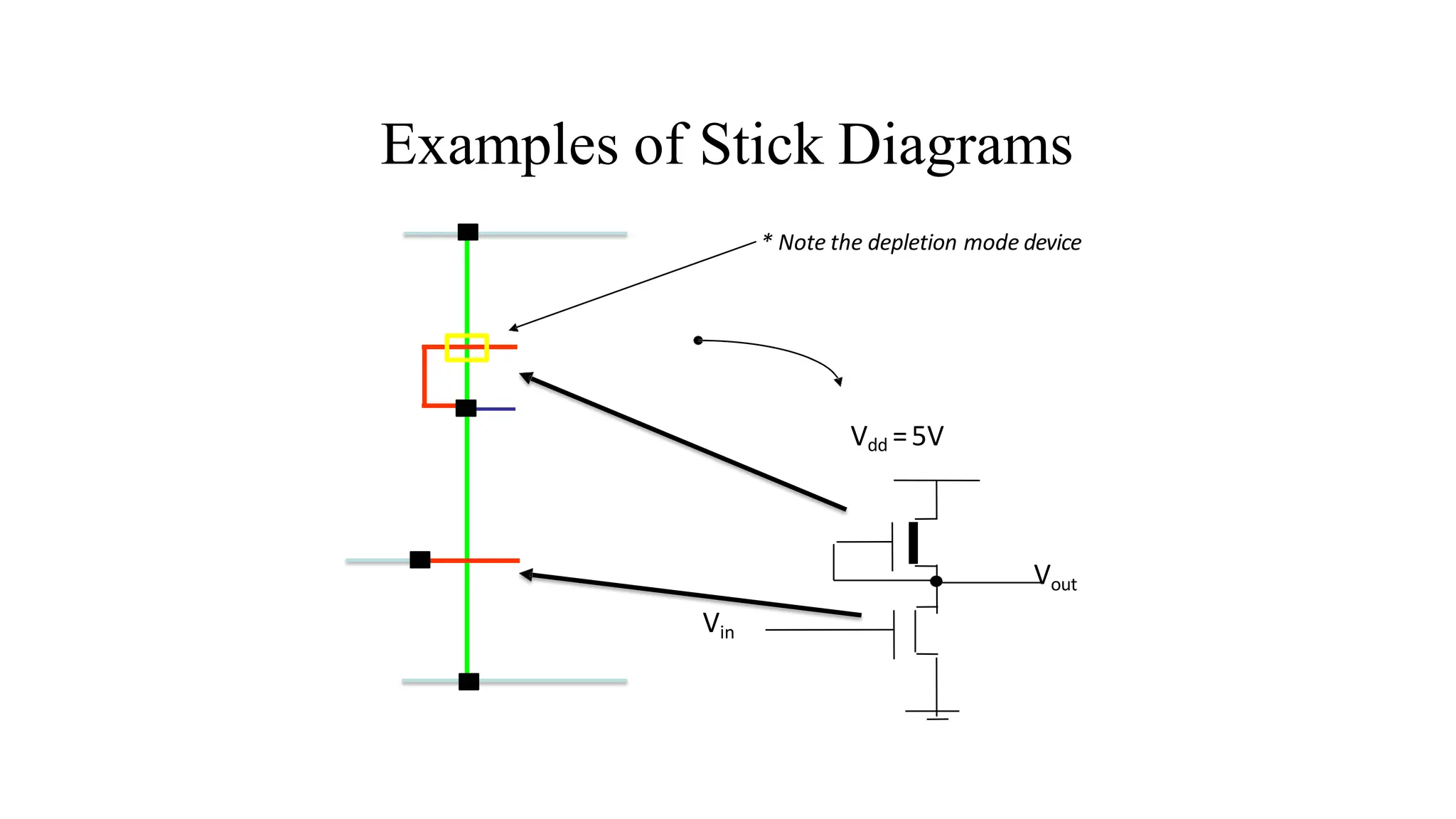
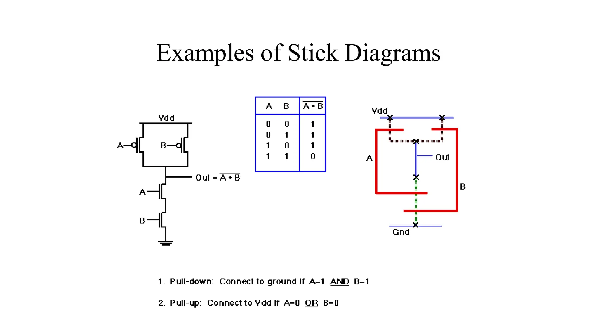
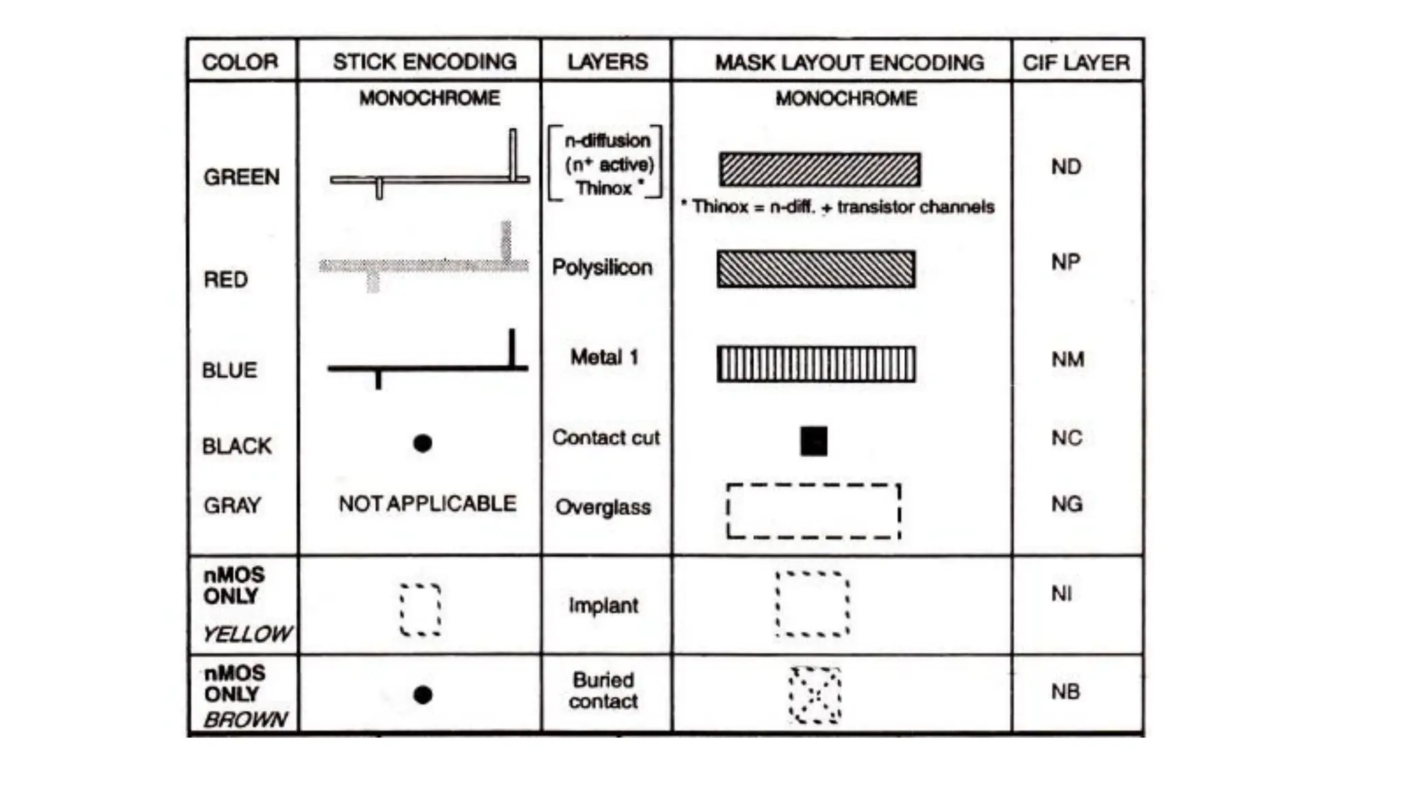
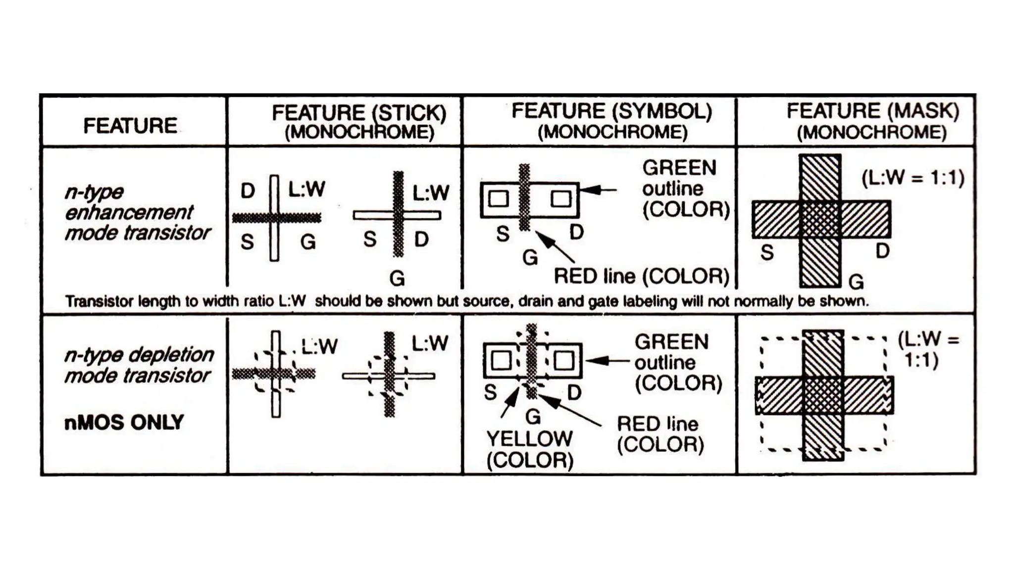
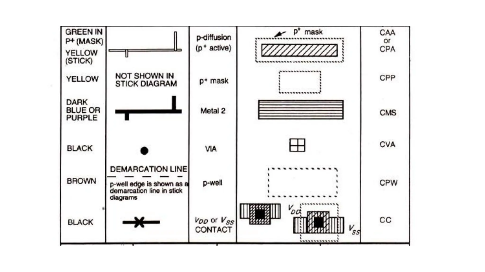
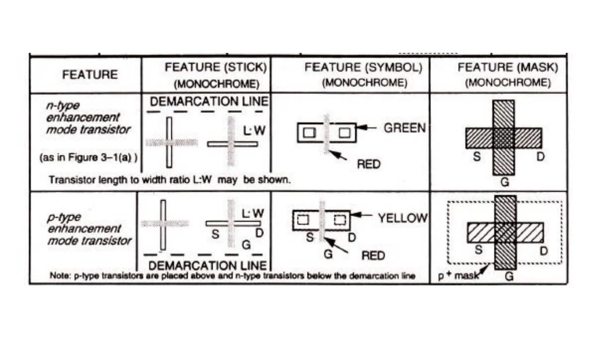
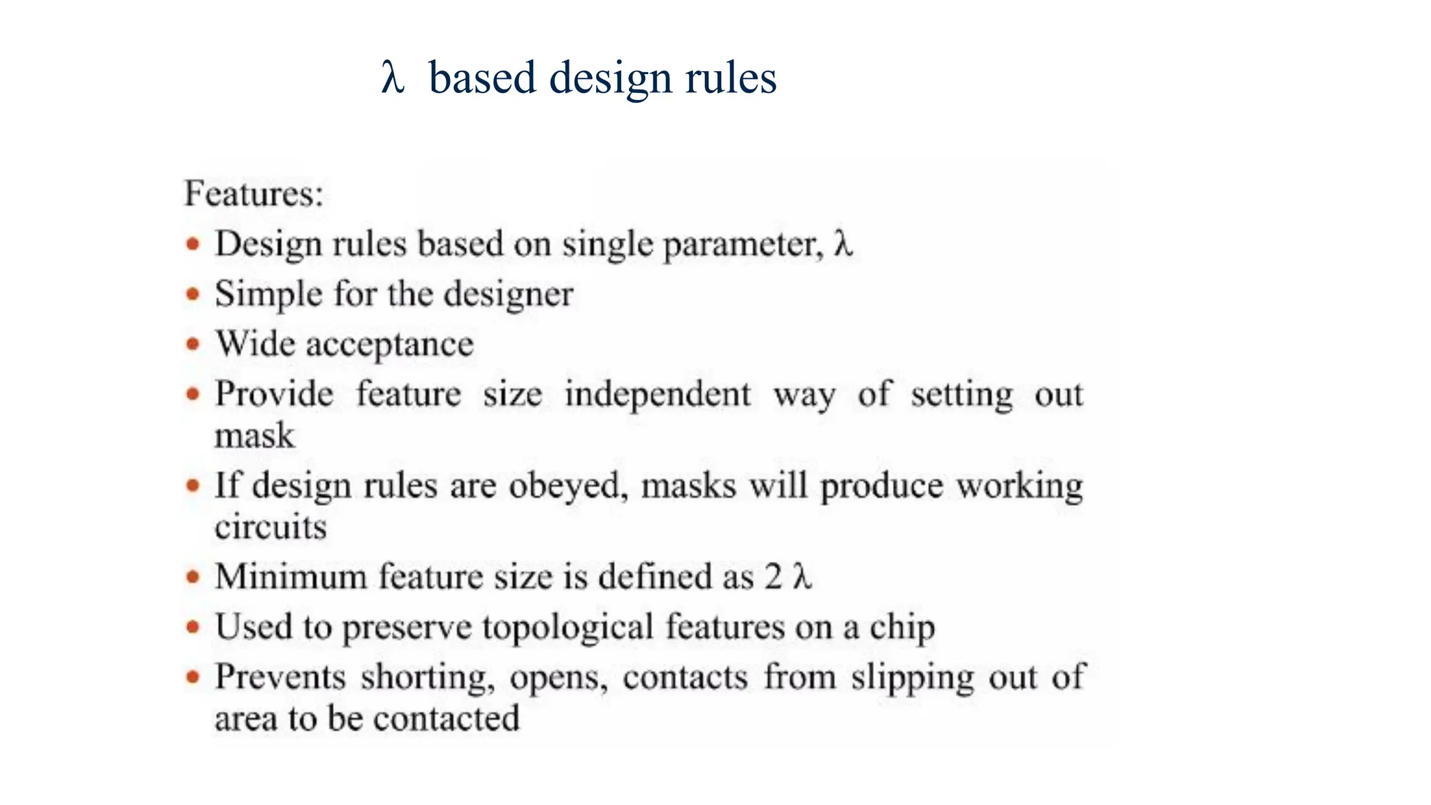
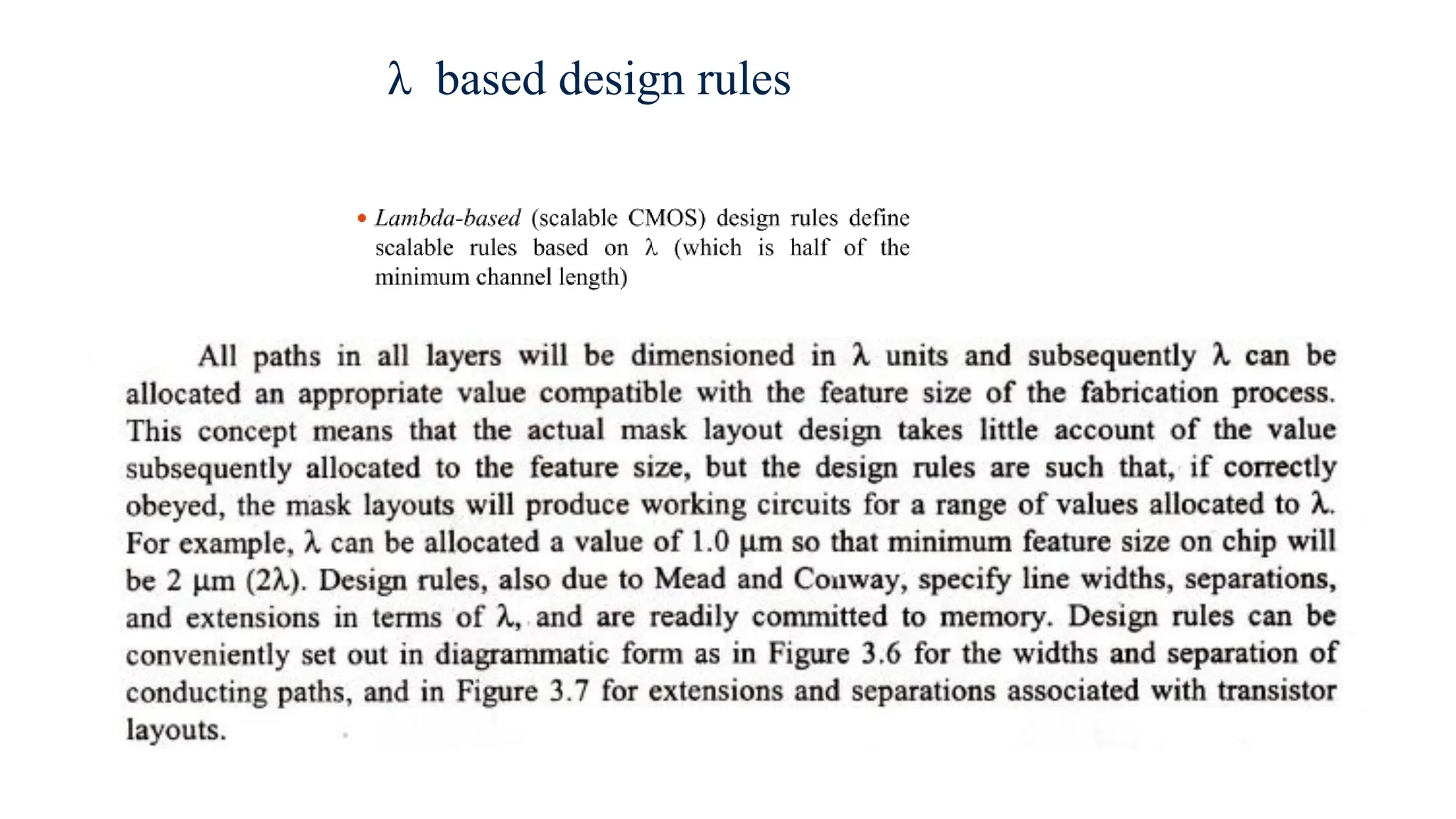
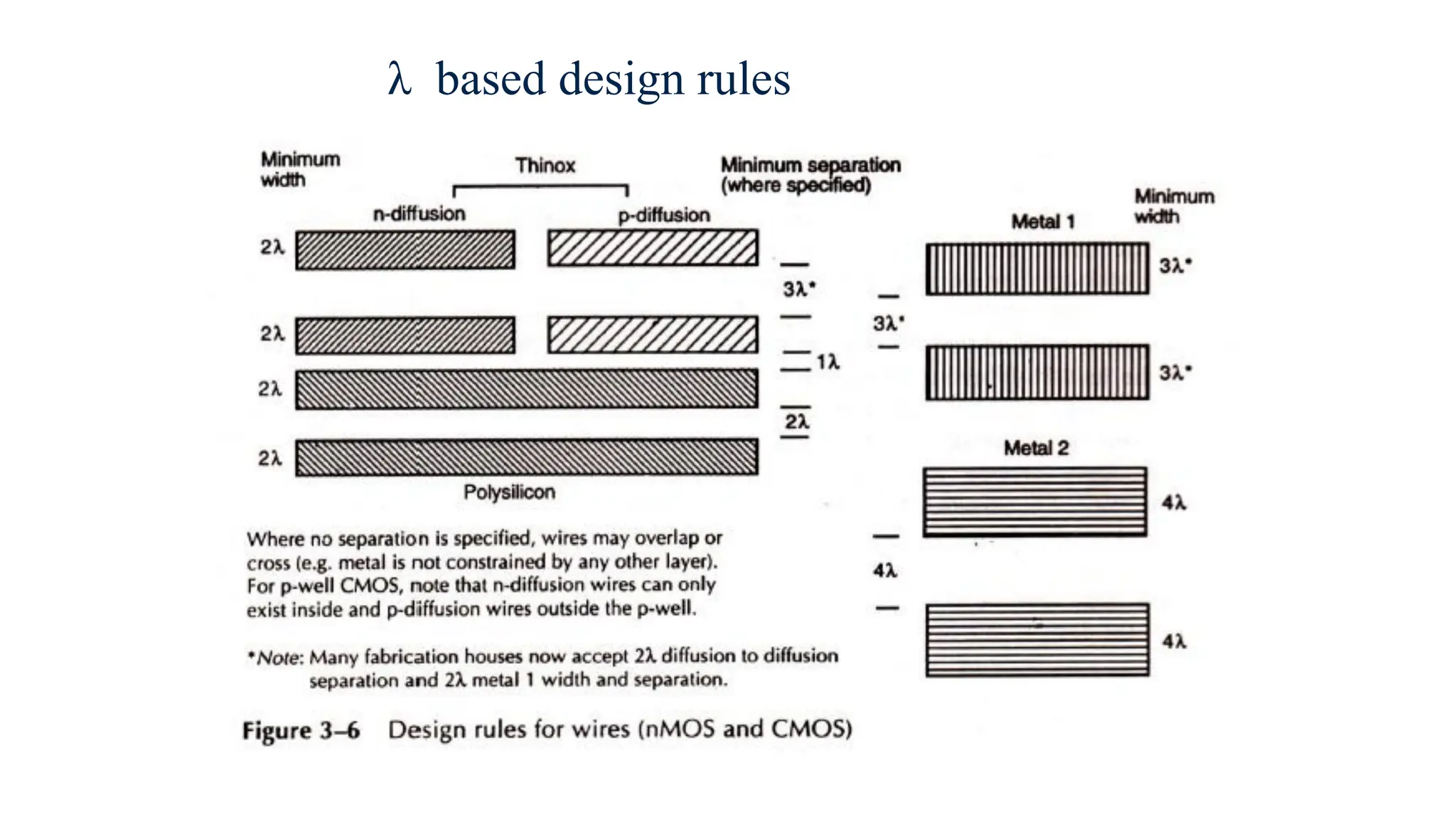
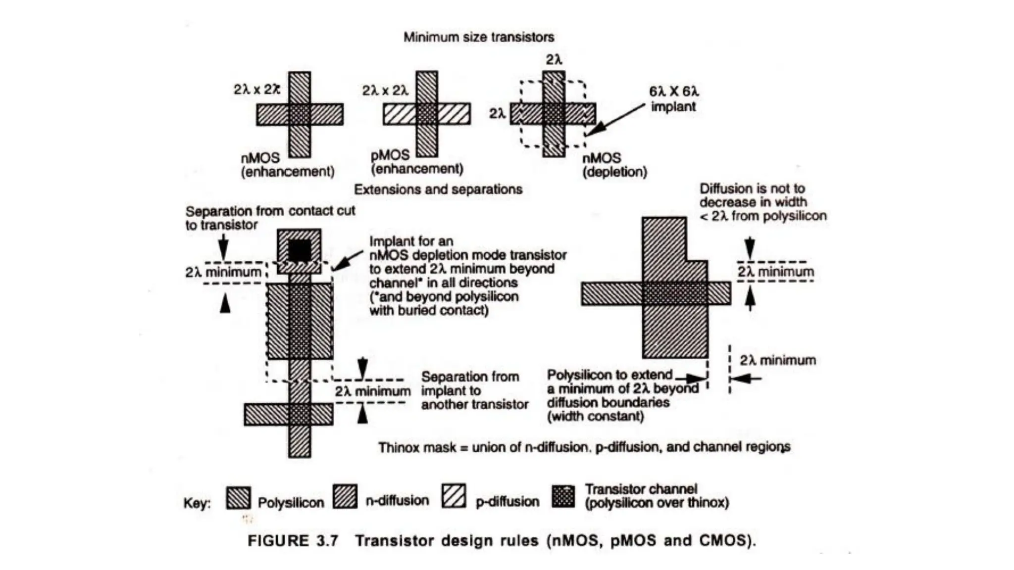
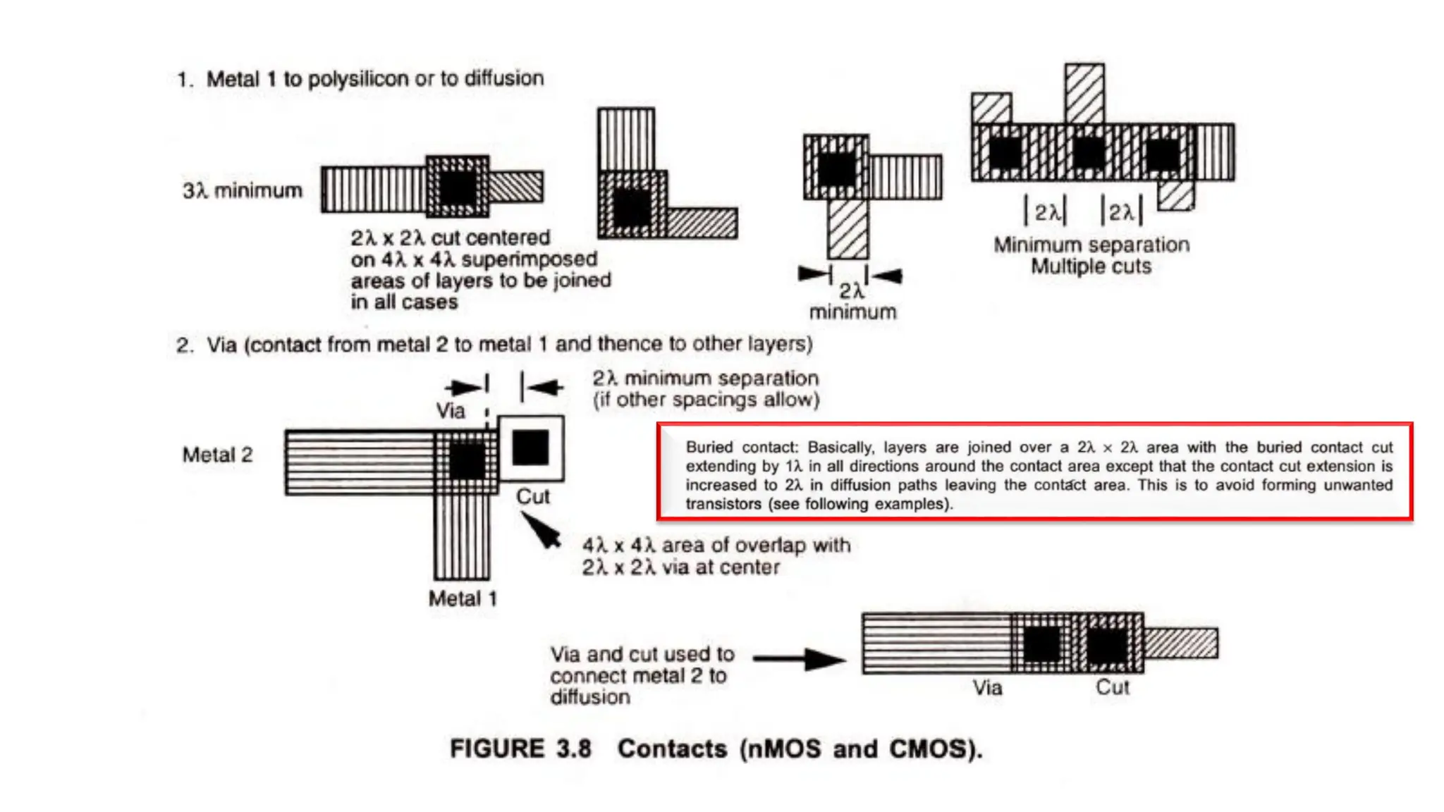
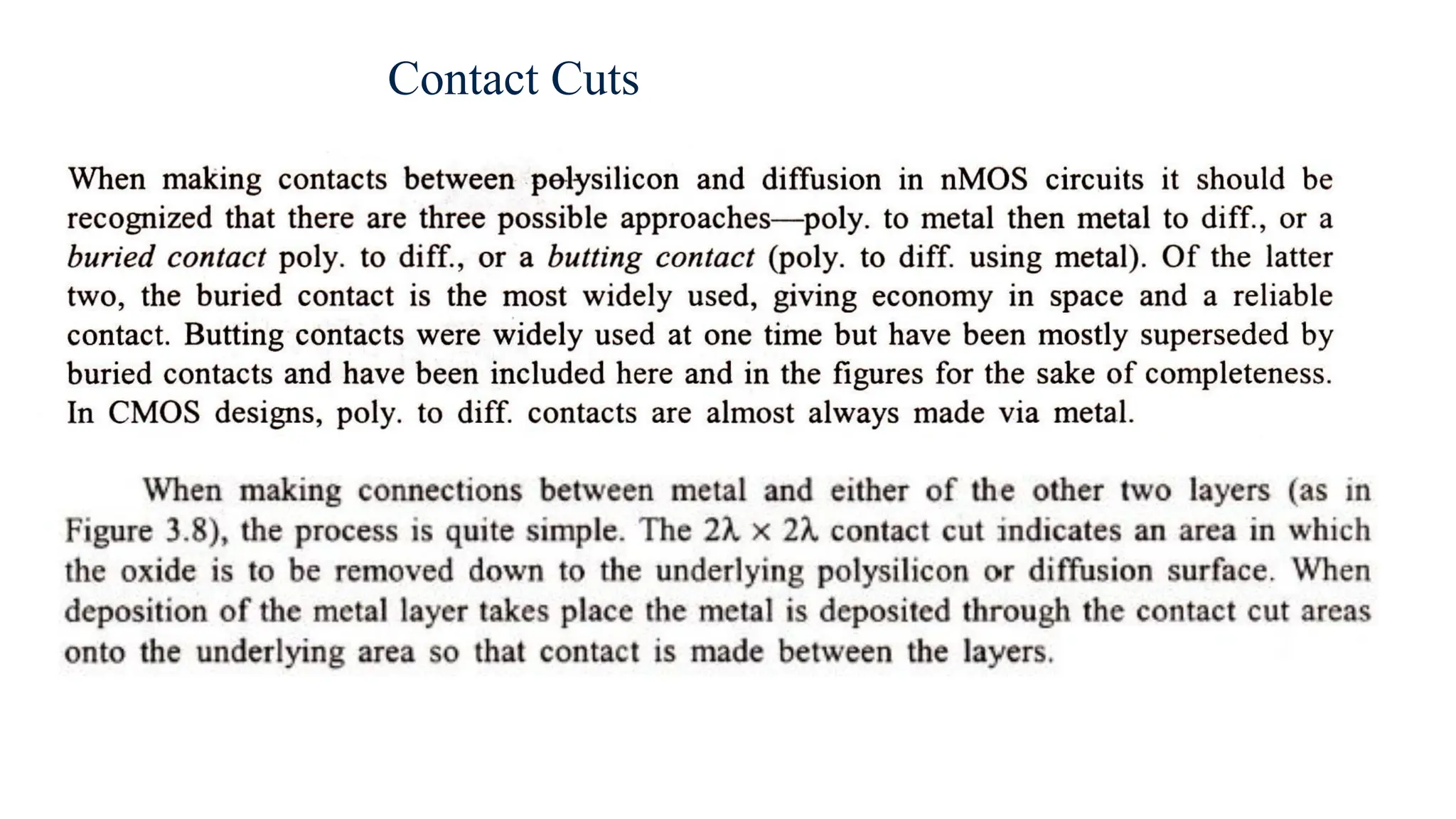
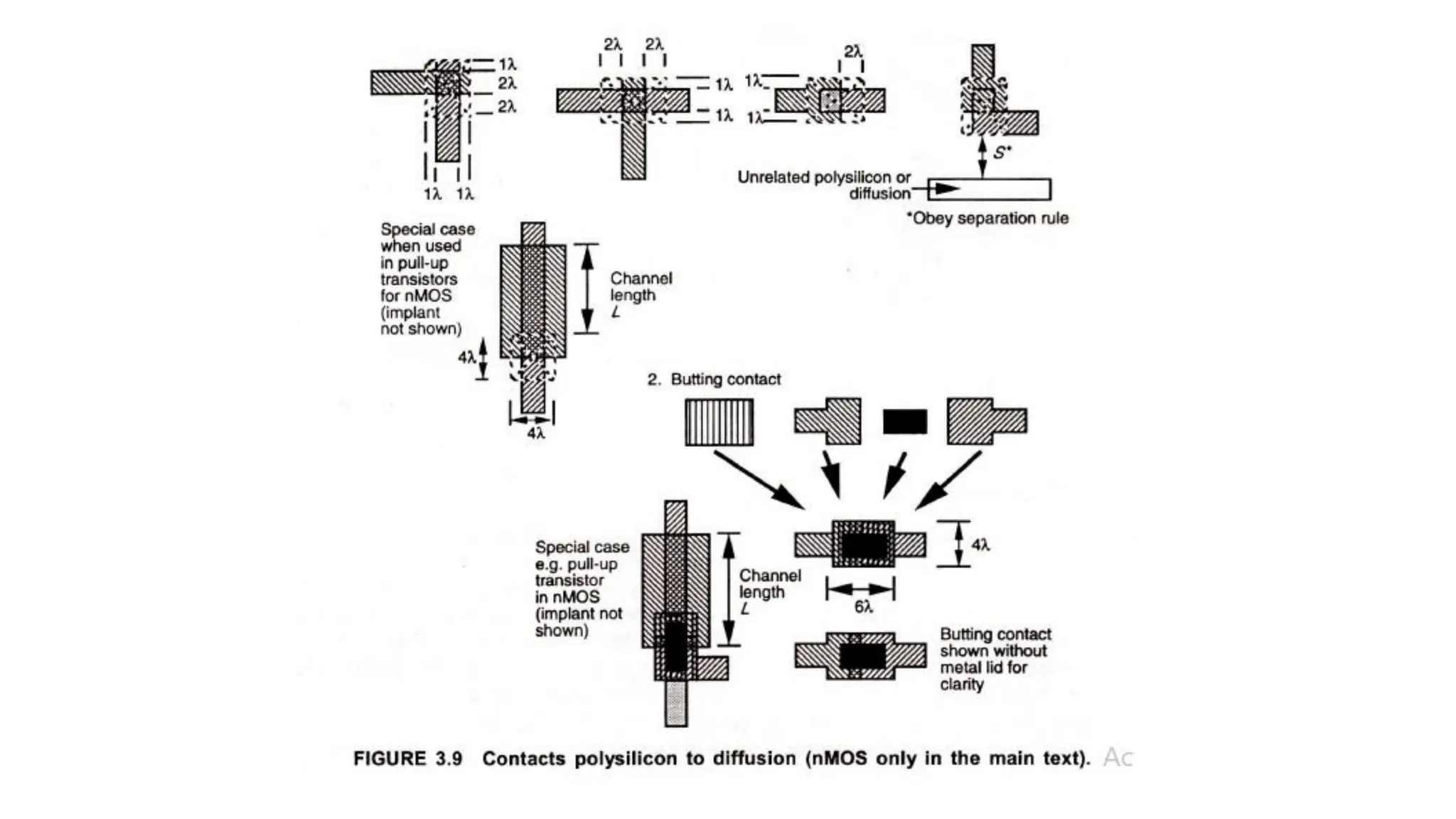
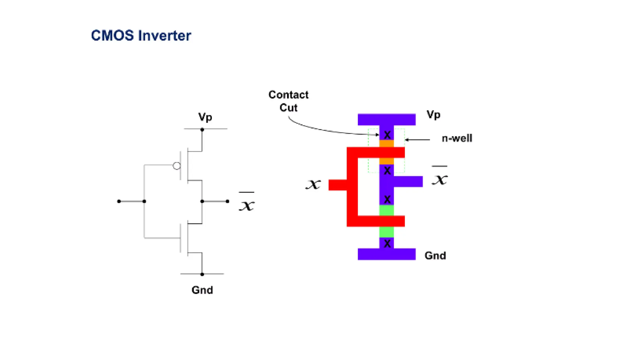
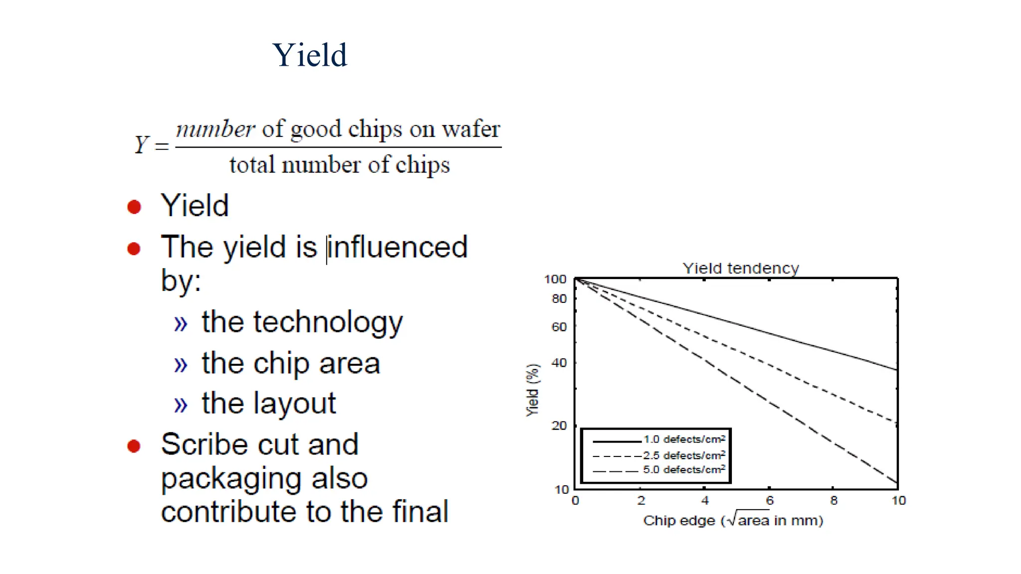
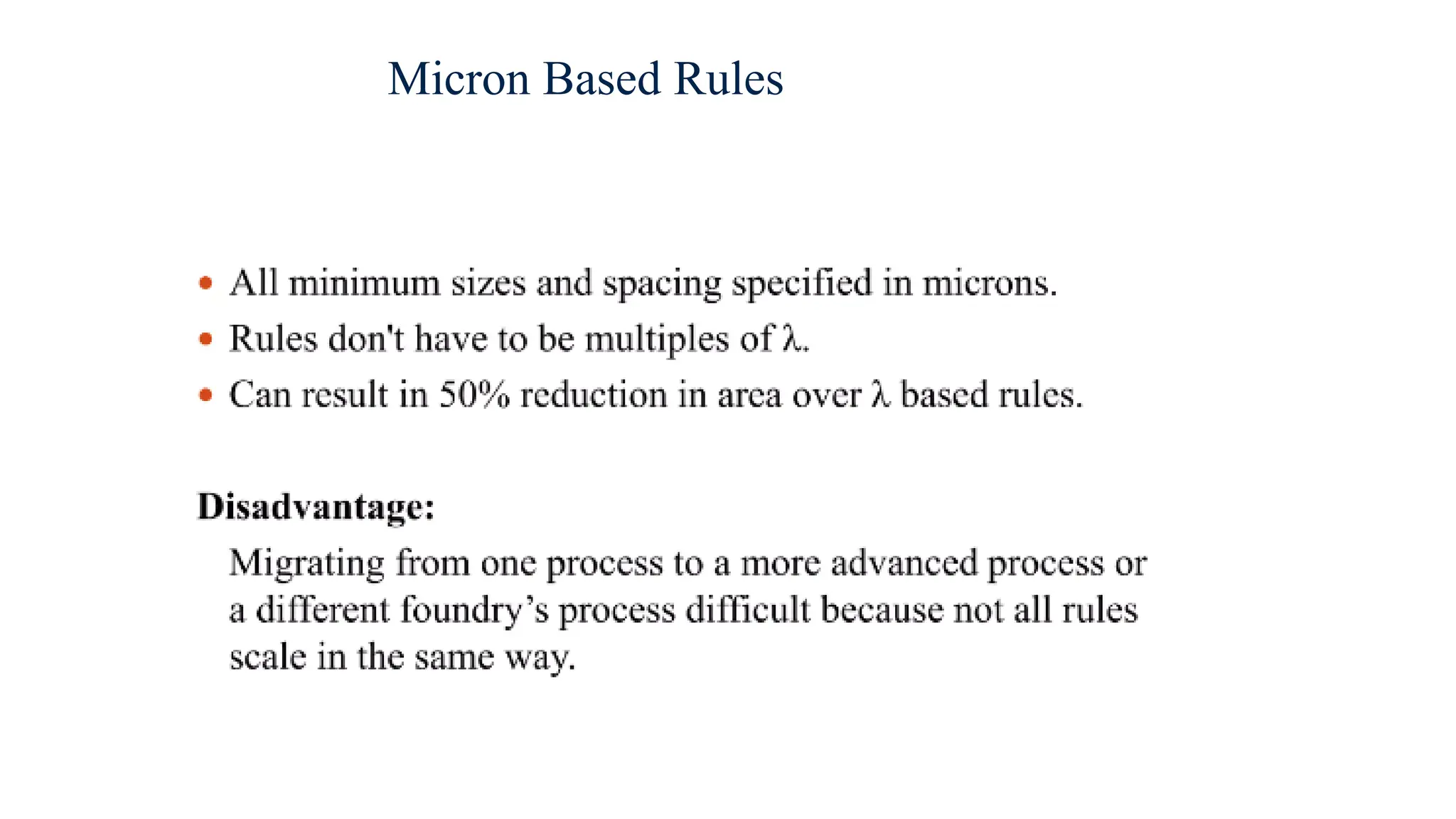
Basics of Stick Diagrams
• VLSI design aims to translate circuit concepts
onto silicon.
• Stick diagrams are a means of capturing
topography and layer information using simple
diagrams.
• Stick diagrams convey layer information
through color
encoding).
codes (or monochrome
• Acts as an interface between symbolic circuit
and the actual layout.
Stick Diagrams
• Does show all components/vias.
– Via is used to connect higher level metals from metal connection
• It shows relative placement of components.
• Goes one step closer to the layout
• Helps plan the layout and routing
A stick diagram is a cartoon of a layout.
Stick Diagrams
• Does not show
– Exact placement of components
– Transistor sizes
– Wire lengths, wire widths, tub boundaries
– Any other low level details such as
parasitics
Stick Diagrams
Stick Diagram Colour Code
P diffusion Yellow/Brown
N diffusion Green
Polysilicon Red
Contacts Black
Metal1 Blue
Metal2 Magenta/Purple
Metal3 Cyan/L.Blue
Metal 1
poly
ndiff
pdiff
Can also draw
in shades of
gray/line style.
Stick Diagrams – Notations
Buried Contact
Contact Cut
Component Colour Use
metal 1 Power and signal wires
metal 2 Power wires
polysilicon Signal wires and transistor
gates
n-diffusion Signal wires,source and drain of
transistors
p-diffusion Signal wires,source and drain of
transistors
contact Signal connection
via Connection between metals
NMOS transistor
PMOS transistor
Stick Diagrams – Some Rules
Rule 1:
When two or more ‘sticks’ of the same type cross or touch
each other that represents electrical contact.
Stick Diagrams – Some Rules
Rule 2:
When two or more sticksof different type cross or touch each
other there is no electrical contact.
(If electrical contact is needed we have to show the connection
explicitly)
Stick Diagrams – Some Rules
Rule 3:
When a poly crosses diffusion it represents a transistor.
Note: If a contact is shown then it is not a transistor.
Stick Diagrams – Some Rules
Rule 4:
In CMOS a demarcation line is drawn to avoid touching of p-diff
with n-diff. All PMOS must lie on one side of the line and all
NMOS will have to be on the other side.
INVERTER- STICK DIAGRAM
Twohorizontal wires are used for connection with VSS and
VDD. This is done in metal2, but metal1can be use instead.
Step 1
Step 2
Two vertical wires (pdiff and ndiff) are used to represent the
p-transistor (yellow) and n-transistor (green).
Step 3
The gates of the transistors are joined with a
polysilicon wire, and connected to the input.
Step 4
. The drains of two transistor are then connected with
metal1 and joined to the output. There cannot be direct
connection from n-transistor to p-transistors.
Step 5
The sources of the transistors are next connectedto
VSS and VDD with metal1. Notice that vias are used, not
contacts
metal1 is used instead of metal2 to connectVSS
and VDD supply
Alternative inverter
NAND Gate
NOR Gate
Examples of Stick Diagrams
Gnd
VDD
x x
X
X
X
X
VDD
x x
Gnd
Examples of Stick Diagrams
Vout
Vdd =5V
Vin
* Note the depletion mode device
Examples of Stick Diagrams
Design Rules
• The limitations of the patterning process give rise to a set of mask design
guidelines called design rules
• Design rules are a set of guidelines that specify the minimum dimensions and
spacings allowed in a layout drawing
• Violating a design rule might result in a non-functional circuit or in a highly
reduced yield
The design rules can be expressed as:
»A list of minimum feature sizes and spacings for all the masks required in a
given process
»Based on single parameter λ that characterize the linear feature (e.g. the
minimum grid dimension). λ base rules allow simple scaling
λ based design rules
Contact Cuts
Double Metal MOS Process
Yield
General Observations of design values
1. Every dimensions must be rounded up to whole lambda
2. The goal of any set of design rules should be to optimized yield while keeping
the geometry as small as possible without compromising the reliability of the
finished circuit.
3. The 3λ metal rules
4. Metal to metal separation is too large.
5. Lambda based rules try “to be all things to all people” they do suffer from
least common denominator effects and from the upward rounding of all
process line dimension parameters into integrer values of lambda.
Design Rules Reality
Micron Based Rules

Stick Diagram presentation slide for VLSI.pdf

  • 1.
  • 2.
    • VLSI designaims to translate circuit concepts onto silicon. • Stick diagrams are a means of capturing topography and layer information using simple diagrams. • Stick diagrams convey layer information through color encoding). codes (or monochrome • Acts as an interface between symbolic circuit and the actual layout. Stick Diagrams
  • 3.
    • Does showall components/vias. – Via is used to connect higher level metals from metal connection • It shows relative placement of components. • Goes one step closer to the layout • Helps plan the layout and routing A stick diagram is a cartoon of a layout. Stick Diagrams
  • 4.
    • Does notshow – Exact placement of components – Transistor sizes – Wire lengths, wire widths, tub boundaries – Any other low level details such as parasitics Stick Diagrams
  • 5.
    Stick Diagram ColourCode P diffusion Yellow/Brown N diffusion Green Polysilicon Red Contacts Black Metal1 Blue Metal2 Magenta/Purple Metal3 Cyan/L.Blue
  • 6.
    Metal 1 poly ndiff pdiff Can alsodraw in shades of gray/line style. Stick Diagrams – Notations Buried Contact Contact Cut
  • 7.
    Component Colour Use metal1 Power and signal wires metal 2 Power wires polysilicon Signal wires and transistor gates n-diffusion Signal wires,source and drain of transistors p-diffusion Signal wires,source and drain of transistors contact Signal connection via Connection between metals
  • 8.
  • 9.
  • 10.
    Stick Diagrams –Some Rules Rule 1: When two or more ‘sticks’ of the same type cross or touch each other that represents electrical contact.
  • 11.
    Stick Diagrams –Some Rules Rule 2: When two or more sticksof different type cross or touch each other there is no electrical contact. (If electrical contact is needed we have to show the connection explicitly)
  • 12.
    Stick Diagrams –Some Rules Rule 3: When a poly crosses diffusion it represents a transistor. Note: If a contact is shown then it is not a transistor.
  • 13.
    Stick Diagrams –Some Rules Rule 4: In CMOS a demarcation line is drawn to avoid touching of p-diff with n-diff. All PMOS must lie on one side of the line and all NMOS will have to be on the other side.
  • 14.
  • 15.
    Twohorizontal wires areused for connection with VSS and VDD. This is done in metal2, but metal1can be use instead. Step 1
  • 16.
    Step 2 Two verticalwires (pdiff and ndiff) are used to represent the p-transistor (yellow) and n-transistor (green).
  • 17.
    Step 3 The gatesof the transistors are joined with a polysilicon wire, and connected to the input.
  • 18.
    Step 4 . Thedrains of two transistor are then connected with metal1 and joined to the output. There cannot be direct connection from n-transistor to p-transistors.
  • 19.
    Step 5 The sourcesof the transistors are next connectedto VSS and VDD with metal1. Notice that vias are used, not contacts
  • 20.
    metal1 is usedinstead of metal2 to connectVSS and VDD supply Alternative inverter
  • 21.
  • 22.
  • 23.
    Examples of StickDiagrams Gnd VDD x x X X X X VDD x x Gnd
  • 24.
  • 25.
    Examples of StickDiagrams Vout Vdd =5V Vin * Note the depletion mode device
  • 26.
  • 31.
    Design Rules • Thelimitations of the patterning process give rise to a set of mask design guidelines called design rules • Design rules are a set of guidelines that specify the minimum dimensions and spacings allowed in a layout drawing • Violating a design rule might result in a non-functional circuit or in a highly reduced yield The design rules can be expressed as: »A list of minimum feature sizes and spacings for all the masks required in a given process »Based on single parameter λ that characterize the linear feature (e.g. the minimum grid dimension). λ base rules allow simple scaling
  • 32.
  • 33.
  • 34.
  • 35.
  • 37.
  • 49.
  • 50.
  • 51.
    General Observations ofdesign values 1. Every dimensions must be rounded up to whole lambda 2. The goal of any set of design rules should be to optimized yield while keeping the geometry as small as possible without compromising the reliability of the finished circuit. 3. The 3λ metal rules 4. Metal to metal separation is too large. 5. Lambda based rules try “to be all things to all people” they do suffer from least common denominator effects and from the upward rounding of all process line dimension parameters into integrer values of lambda.
  • 52.
  • 55.