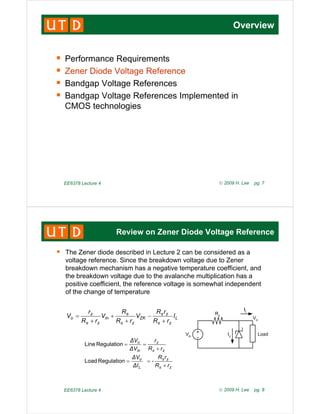
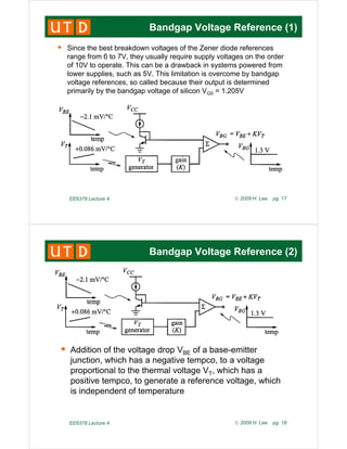
This document provides an overview of voltage references and describes a lecture on bandgap voltage references. It discusses the performance requirements of voltage references including accuracy, stability, load regulation, and thermal stability. It then summarizes zener diode references and describes how a bandgap voltage reference works by combining the positive temperature coefficient of thermal voltage VT with the negative coefficient of the base-emitter voltage VBE to produce an output voltage independent of temperature. The document explains the fundamentals and shows a bandgap voltage reference circuit using two bipolar transistors with different emitter areas to generate proportional to absolute temperature (PTAT) and complementary to absolute temperature (CTAT) voltages.


![Load Regulation (1)
ƒ The load regulation is directly related to the output
impedance. To find Ro, we suppress the input source
Vz and apply the test-voltage technique. By voltage
divider formula:
divider formula:
v
R
r
R
r
R
v
in
in
N
2
1
1
//
//
+
=
ƒ Summing currents at the output node
0
=
−
−
+
−
+ N
N v
Av
v
v
i
ƒ Eliminating vN and solving for the Ro=v/I, we obtain
0
2
=
+
+
o
r
R
i
1
2
1
2
1
where
)]
/
/
1
/(
)
/
/
[(
1
R
b
r
r
R
R
R
r
r
R
r
A
r
R
o
in
in
o
o
o
o
=
≈
+
+
+
+
+
=
EE6378 Lecture 4 © 2009 H. Lee pg. 11
2
1
where
1 R
R
b
Ab +
+
Load Regulation (2)
ƒ Typically rin is in the MΩ range or
greater, R1 and R2 are in kΩ range
and ro is on the order of 102 Ω. The
t /R / d R / th
terms ro/R1, ro/rin, and R2/rin can thus
be ignored to yield Ro≈ro/(1+Ab)
ƒ The load regulation R r /(1+Ab)
ƒ The load regulation Ro≈ro/(1+Ab)
which is much smaller than the Zener
diode voltage reference without
opamp
p p
ƒ Since ro and A are frequency
dependent, so are the load
regulation. In general, load regulation
tends to degrade with frequency
EE6378 Lecture 4 © 2009 H. Lee pg. 12](https://image.slidesharecdn.com/ee6378bandgapreference-220317062427/85/Ee6378-bandgap-reference-6-320.jpg)
![Thermal Stability (1)
ƒ Thermal stability is one of the most demanding performance
requirement of voltage references due to the fact that semiconductor
components are strongly influenced by temperature
ƒ The for ard bias oltage V and c rrent I of a silicon pn j nction
ƒ The forward-bias voltage VD and current ID of a silicon pn junction,
which forms the basis of the diodes and BJTs, are related as
VD=VTln(ID/IS), where VT is the thermal voltage and IS is the saturation
current. Their expressions are
p
where
)
/
exp(
and
/ 0
3
T
G
S
T V
V
BT
I
q
kT
V −
=
=
k=1.381×10⁻²³ is Boltzmann’s constant
q=1.602 ×10⁻²³ C is the electron charge
T is the absolute temperature
p
B is a proportionality constant
VG0 = 1.205V is the bandgap voltage for silicon
EE6378 Lecture 4 © 2009 H. Lee pg. 13
Thermal Stability (2)
ƒ The temperature coefficient (TC) of the thermal voltage:
C
mV/
0862
0
)
(
TC o
=
=
∂
=
k
V
V T
T C
mV/
0862
.
0
)
(
TC =
=
∂
=
q
T
VT
)
3
(
)
ln
3
(
]
[ln
)
ln(
)
(
TC 0
0
k
V
V
V
V
T
V
V
I
I
V
I
V
V D
G
T
G
D
S
D
D
T
+
−
=
−
∂
=
∂
+
∂
=
Assume VD=650mV at 25oC, we get TC(VD) ≈ -2.1mV/oC.
)
-(
)
ln(
)
(
TC
q
T
T
V
T
T
V
I
T
V T
T
S
D +
=
∂
−
=
∂
+
∂
=
ƒ TC(VT) have a positive tempco and TC(VD) have a negative tempco,
so these two equations form the basis of two common approaches to
thermal stabilization, namely, thermal compensated Zener diode
, y, p
references and bandgap references
EE6378 Lecture 4 © 2009 H. Lee pg. 14](https://image.slidesharecdn.com/ee6378bandgapreference-220317062427/85/Ee6378-bandgap-reference-7-320.jpg)


![Offset Voltage Consideration
1
2
ln( )
( )[ ln( ) ]
T OFF
V N V
I
R
R
V V V N V
+
=
⇒ + +
A l N i d t i i i
2
2
1
( )[ ln( ) ]
ref EB T OFF
V V V N V
R
⇒ = + ⋅ +
ƒ A larger N is used to minimize
the required R2/R1, and the
effect of the amplifier offset
I hi
ƒ Increase chip area
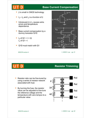
EE6378 Lecture 4 © 2009 H. Lee pg. 39
Base Resistance Consideration
ƒ Large base resistance of
parasitic vertical BJT
ƒ Diode-connected BJT ≠ VEB
ƒ As mentioned before, I <
0.1mA
ƒ Not due to low-power
design, but due to reduce
voltage across RB
ƒ On layout, more N-well
contacts to reduce RB
EE6378 Lecture 4 © 2009 H. Lee pg. 40](https://image.slidesharecdn.com/ee6378bandgapreference-220317062427/85/Ee6378-bandgap-reference-20-320.jpg)