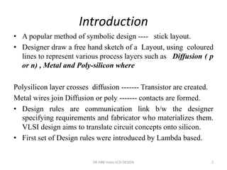
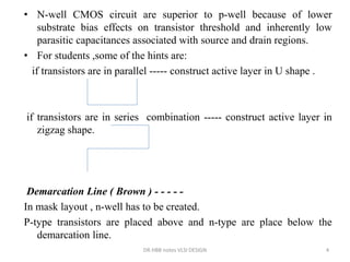
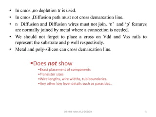
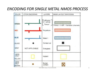
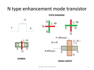
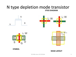
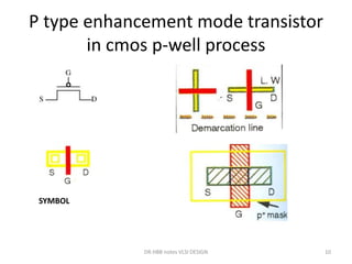
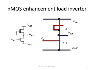
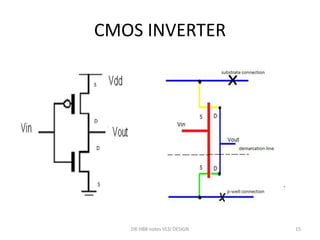
1) Stick diagrams are a popular method for symbolically designing VLSI layouts using colored lines to represent different layers like diffusion, metal, and polysilicon.
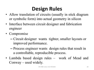
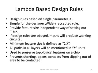
2) Design rules are used to communicate requirements between designers and fabricators to ensure layouts can be successfully materialized in silicon.
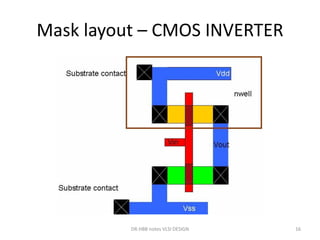
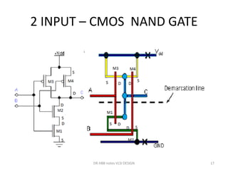
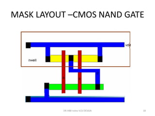
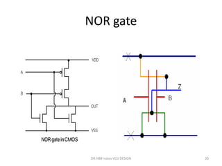
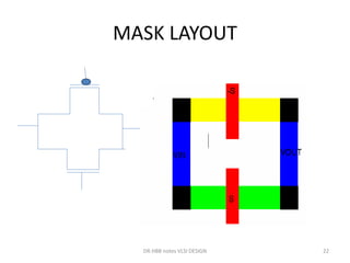
3) Stick diagrams convey layer information through color coding and are essentially the same as mask layouts but must show aspect ratios and dimensions between features for fabrication.


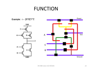
![stick diagram nMOS implementation
of the function f’ = [(x.y)+z]
DR.HBB notes VLSI DESIGN 24](https://image.slidesharecdn.com/vlsi-module-3-230810115728-8a8e796f/85/VLSI-Module-3-pdf-24-320.jpg)