VLSI circuit design involves a standardized process of scaling down transistor sizes over multiple generations. This document outlines key aspects of the VLSI design process including:
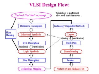
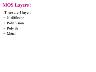
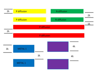
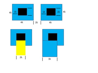
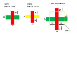
1) MOSFET layers, stick diagrams, design rules and layout diagrams are used to plan and design VLSI circuits before fabrication.
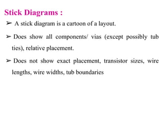
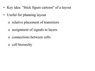
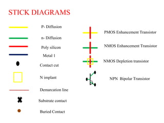
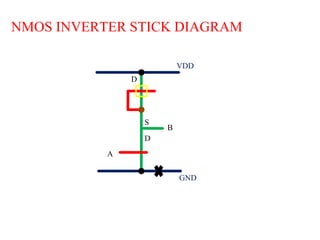
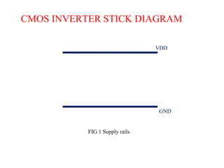
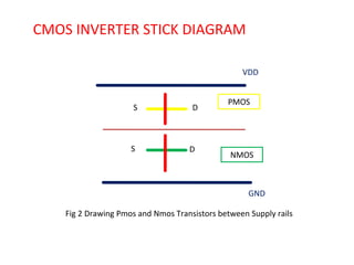
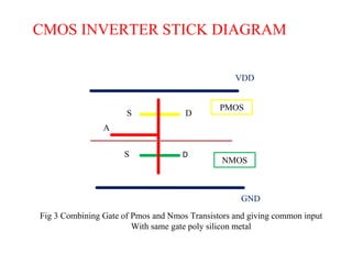
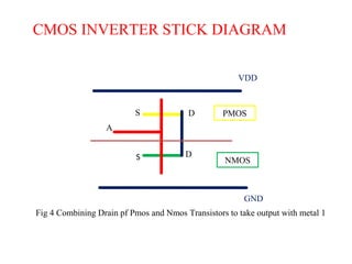
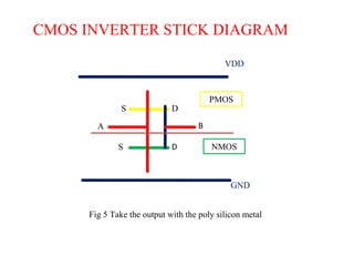
2) Stick diagrams provide a simplified cartoon view of layouts showing relative placement of transistors without exact sizes or spacings.
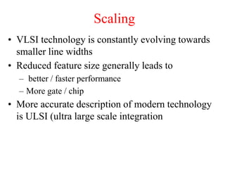
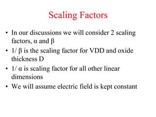
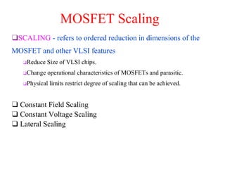
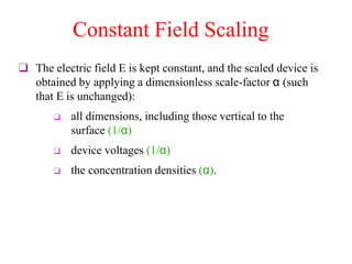
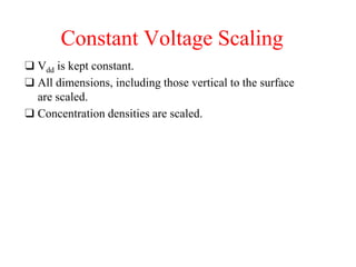
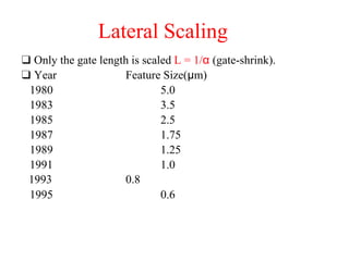
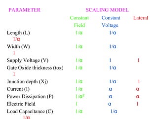
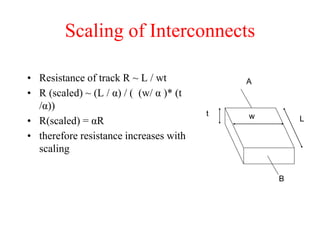
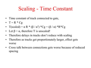
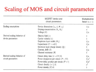
3) Scaling down transistor dimensions according to standard scaling factors allows more transistors to fit on chips leading to improved performance over generations, but also introduces challenges like increased interconnect delays and crosstalk.