This document summarizes the basics of SRAM and DRAM memories. It discusses the architecture and operation of SRAM, including the typical components of an SRAM like the memory array, row and column decoders, sense amplifiers, and timing diagrams for read and write cycles. It also explains the basic 6T SRAM memory cell design and its read and write operations. Finally, it briefly mentions future trends in DRAM development.
LPVLSI
Module V: Low-VoltageLow-Power Memories
Basics of SRAM, Memory Cell, Precharge
and Equalization Circuit
Low-Power SRAM Technologies
Basics of DRAM
Self-Refresh Circuit
Future Trend and Development of
DRAM.
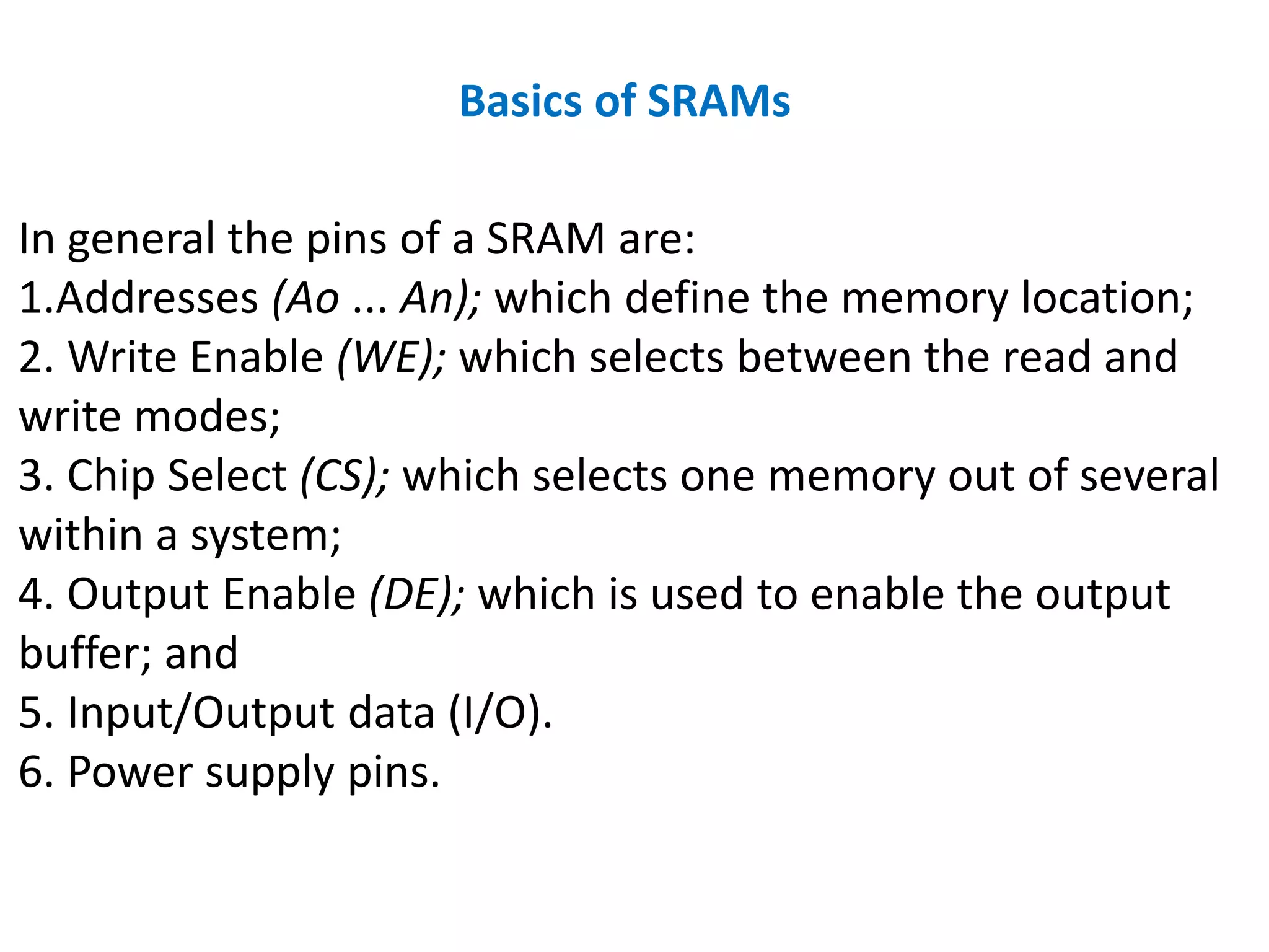
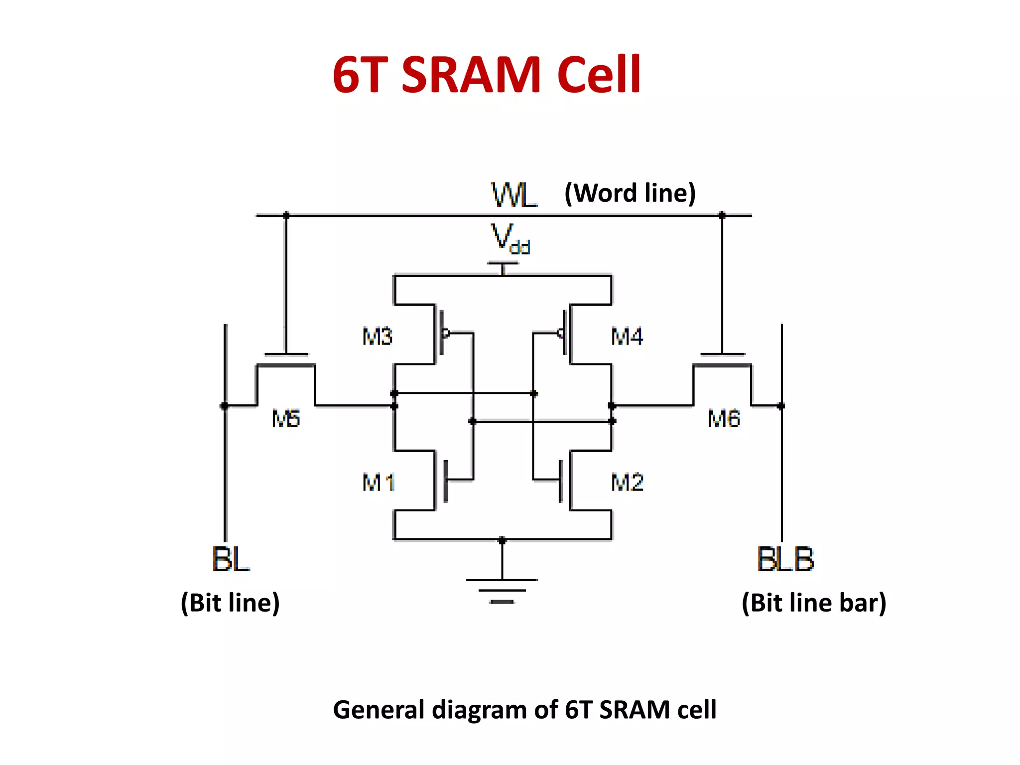
Basics of SRAMs
Ingeneral the pins of a SRAM are:
1.Addresses (Ao ... An); which define the memory location;
2. Write Enable (WE); which selects between the read and
write modes;
3. Chip Select (CS); which selects one memory out of several
within a system;
4. Output Enable (DE); which is used to enable the output
buffer; and
5. Input/Output data (I/O).
6. Power supply pins.
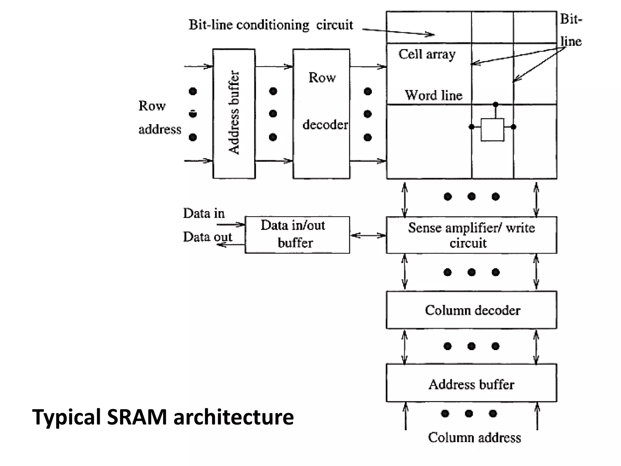
The memory arraycontains the memory cells
which are readable and writable.
The row decoder (X-decoder) selects I out of
n = 2K rows, while the column decoder (Y-
decoder) selects I = 2i out of m = 2j columns.
The address (row and column) are not
multiplexed as in the case of a DRAM.
Sense amplifiers detect small voltage
variations on the memory complementary
bit-line which reduces the reading time.
6.
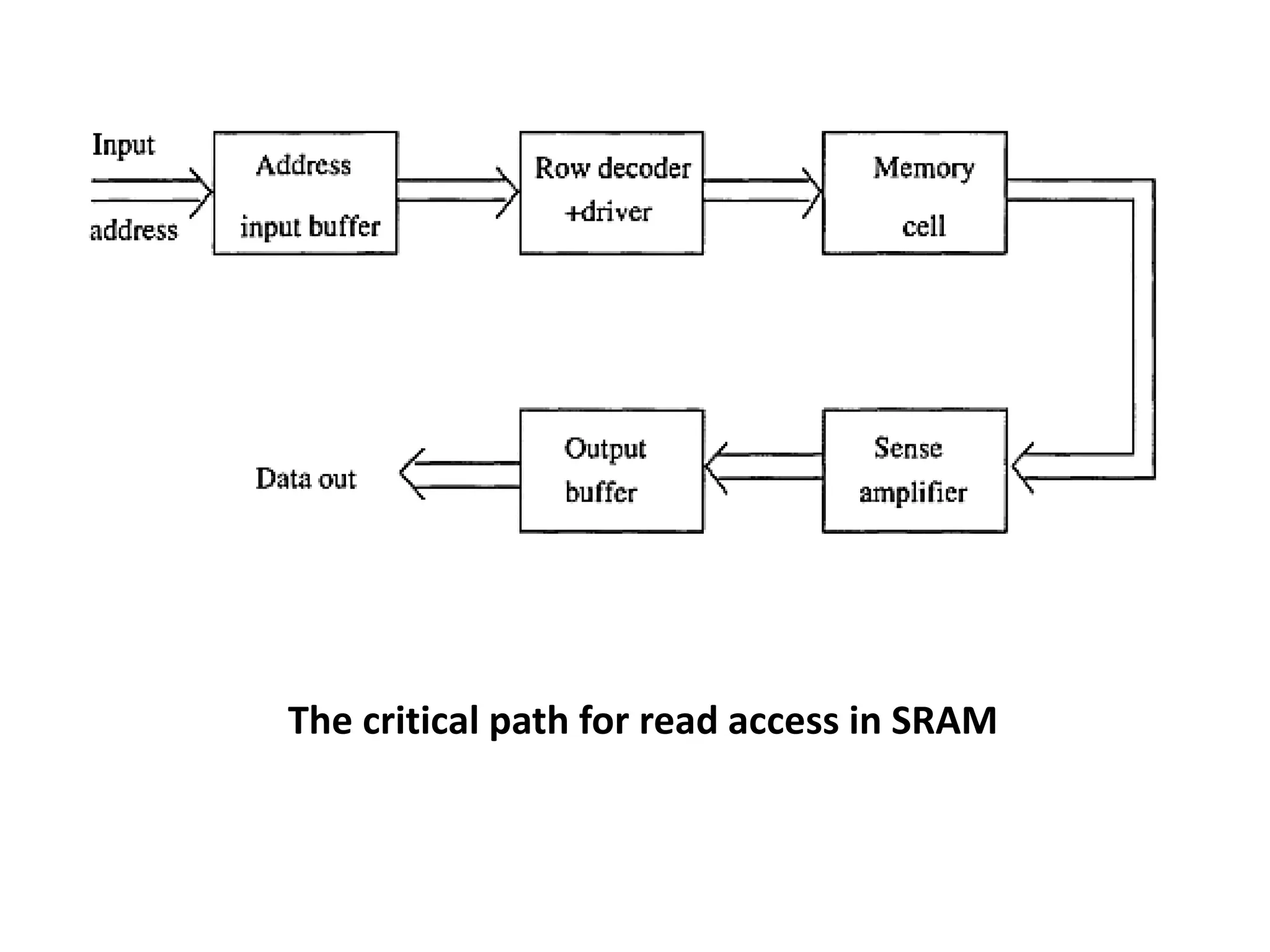
The conditioning circuitpermits the
precharge of the bit-lines.
The access time is determined by the critical
path from the address input to the data
output as shown below.
This path contains address input buffer, row
decoder, memory cell array, sense amplifier
and output buffer circuits.
The word-line decoding and bit-lines sensing
delay times are critical delay components.
7.
To reduce thesensing time during a read
operation, the swing on the bit-lines should
be as small as possible.
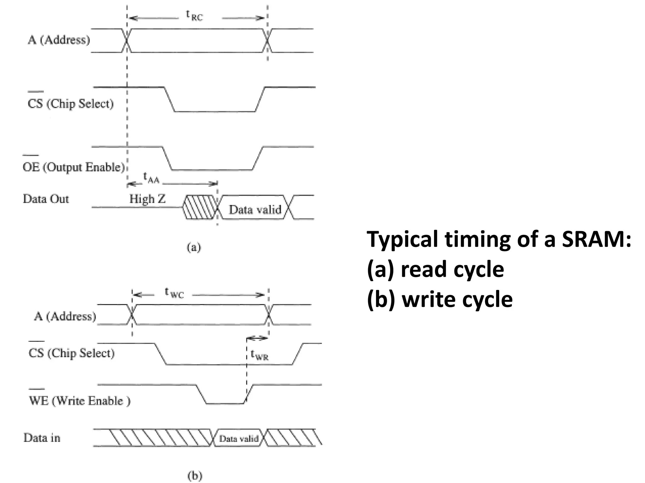
A timing diagramduring read cycle is shown above.
During this time the data stored in a specific
SRAM location (defined by the address) is read
out.
For a read cycle, two times are shown in the
figure; the read cycle time, tRC, and the address
access time, tAA.
Figure shows the write cycle which permits
change to the data in an SRAM.
Two times are indicated, the write cycle time, tWC,
and the write recovery time, tWR.


![MID_TERM_PPT[1].pdf128228282828828282828282](https://cdn.slidesharecdn.com/ss_thumbnails/midtermppt1-250106164820-22402fb8-thumbnail.jpg?width=640&height=640&fit=bounds)