Downloaded 11 times


The document provides an overview of VLSI (Very Large Scale Integration) circuit design and associated technologies including various types of integrated circuits, such as processors, memory chips, and embedded systems. It discusses Moore's Law and its historical significance in predicting the growth of transistor density and performance over time, alongside a brief history of significant advancements in transistor technology. Additionally, it touches upon key figures in semiconductor history, including Julius Edgar Lilienfeld and the development of the first transistors and integrated circuits.
Introduction to VLSI Circuit Design, focusing on Very Large Scale Integration.
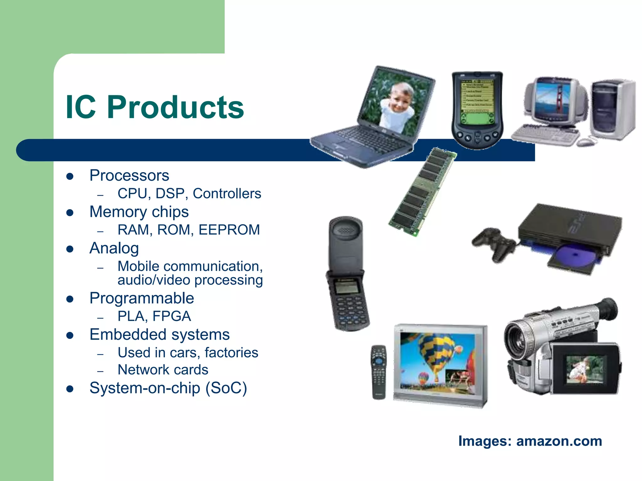
Overview of various IC products including processors, memory chips, analog devices, programmable devices, and embedded systems.
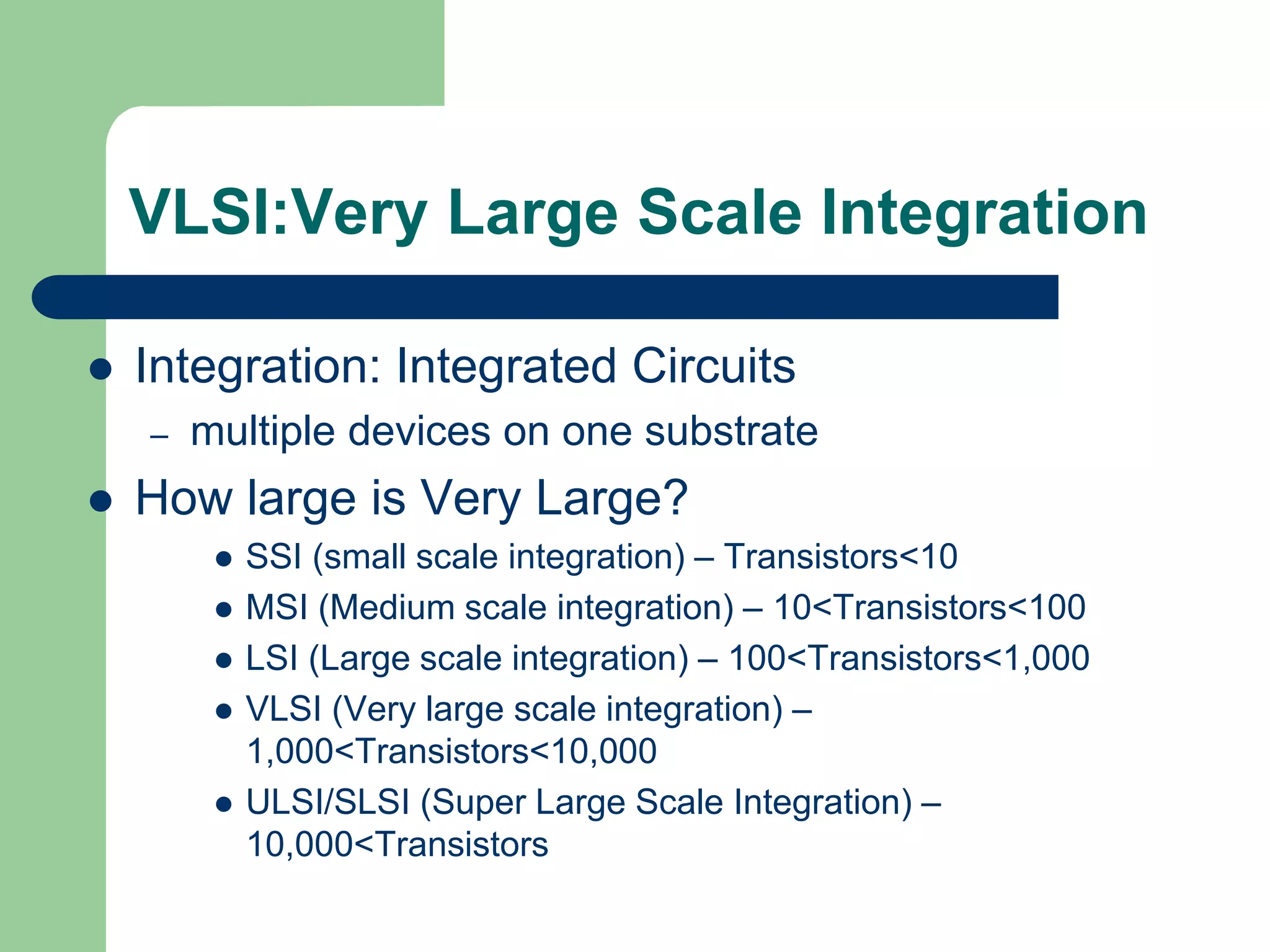
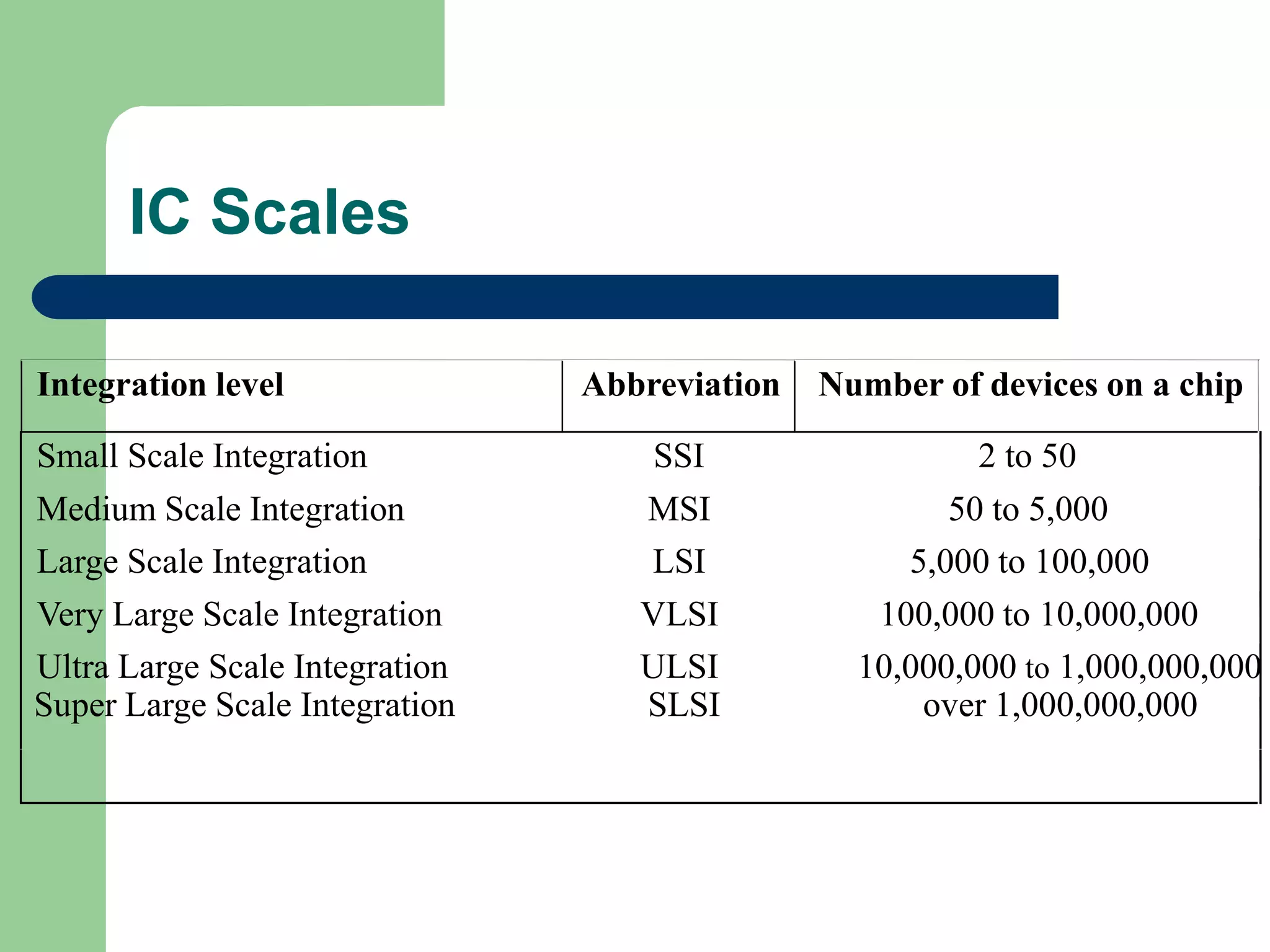
Definition of VLSI - Very Large Scale Integration and explanation of different integration scales from SSI to ULSI.
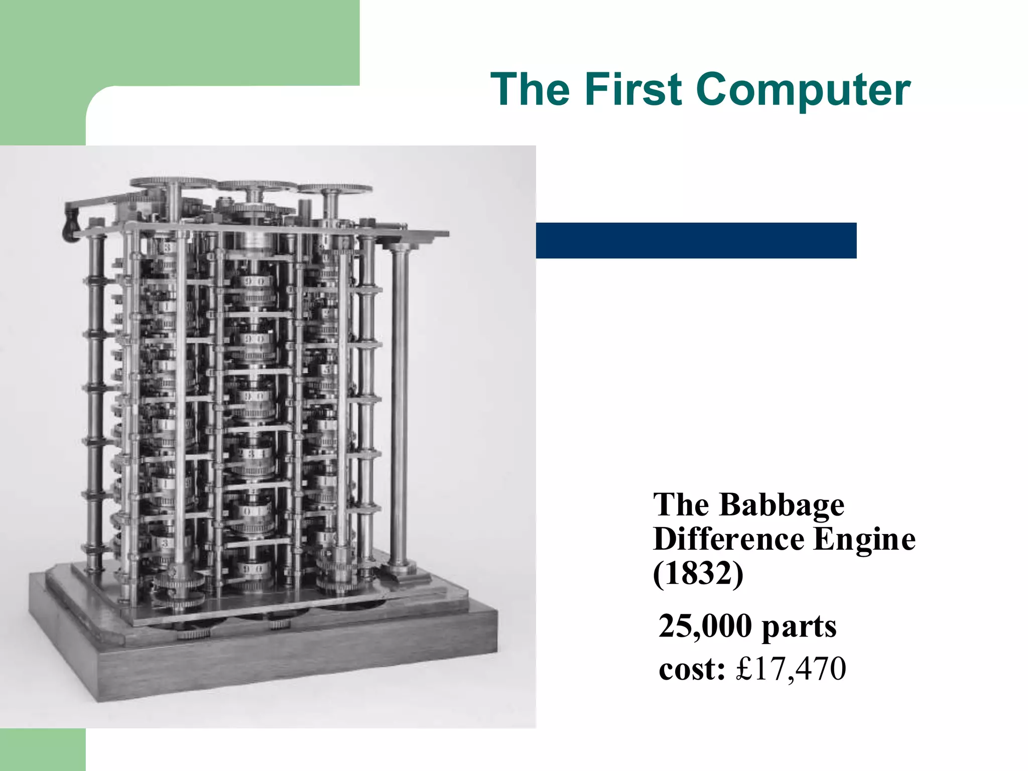
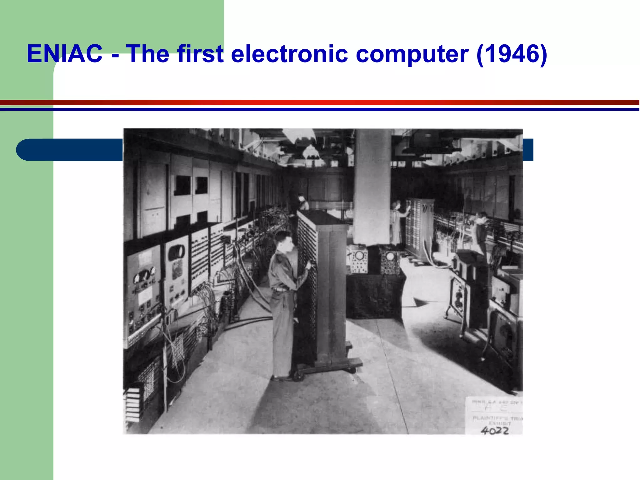
Achievements in early computing, highlighting Charles Babbage's Difference Engine and ENIAC as significant milestones.
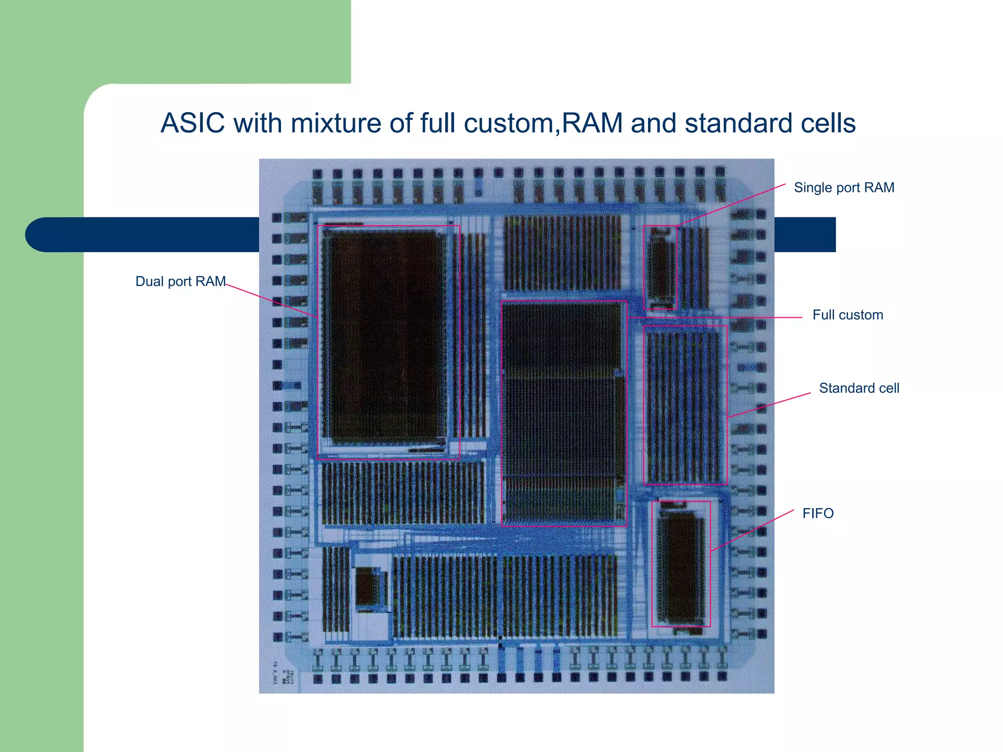
Different types of memory configurations like Dual port RAM, FIFO, and ASIC components.
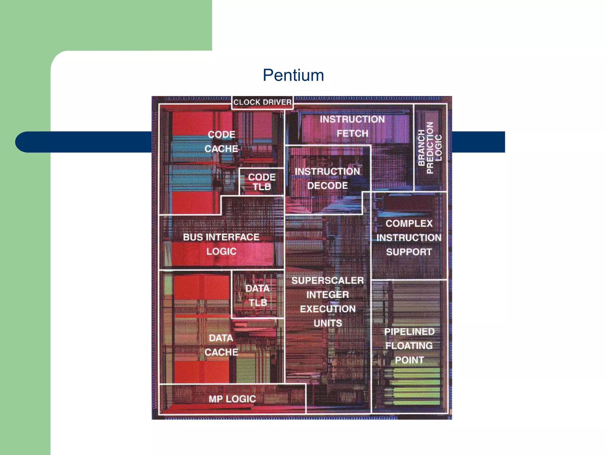
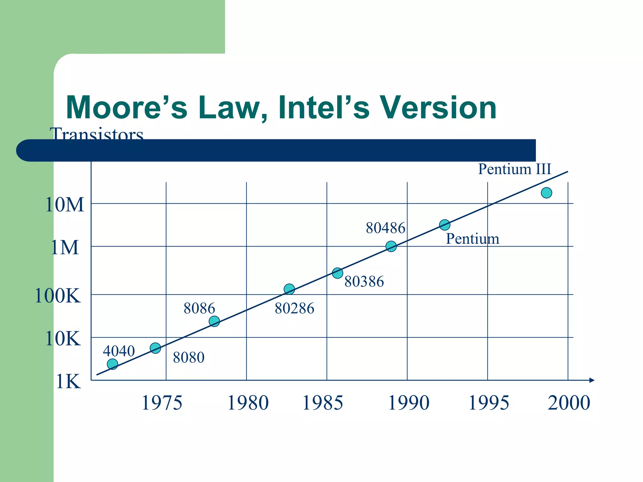
Introduction to the Pentium microprocessor, a significant development in VLSI technology.
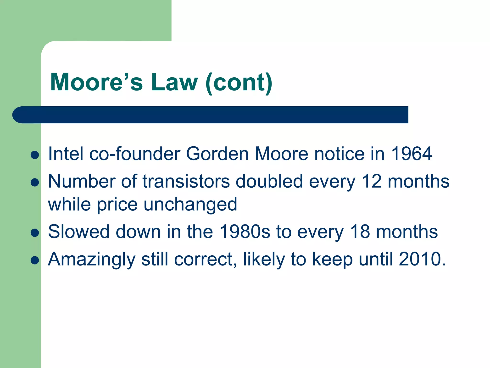
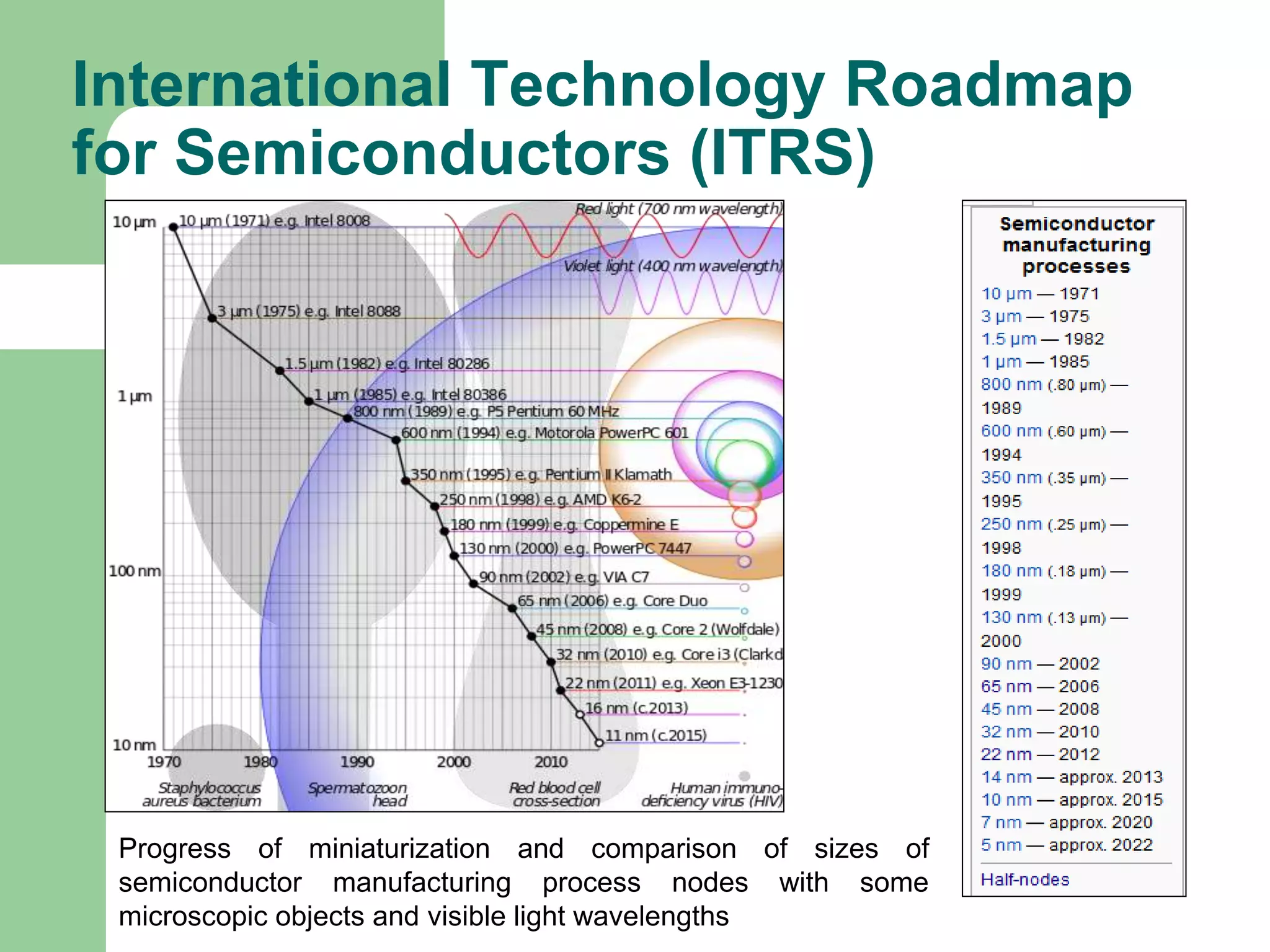
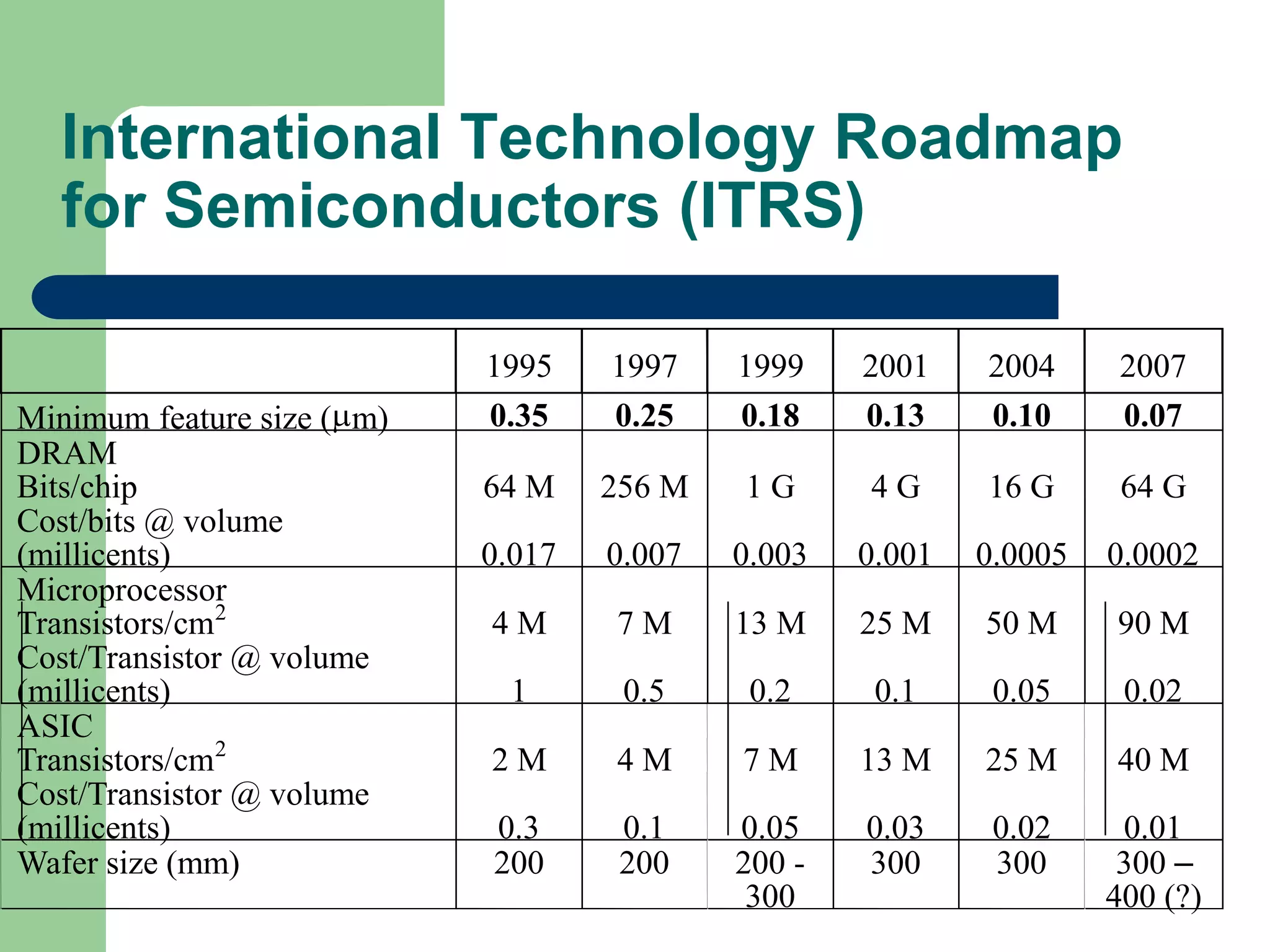
Presentation of Moore's Law stating the doubling of transistor density and performance every 18-24 months, and discussing its implications and limitations. Details on IC scales from SSI to SLSI and an overview of the International Technology Roadmap for Semiconductors comparing manufacturing processes.
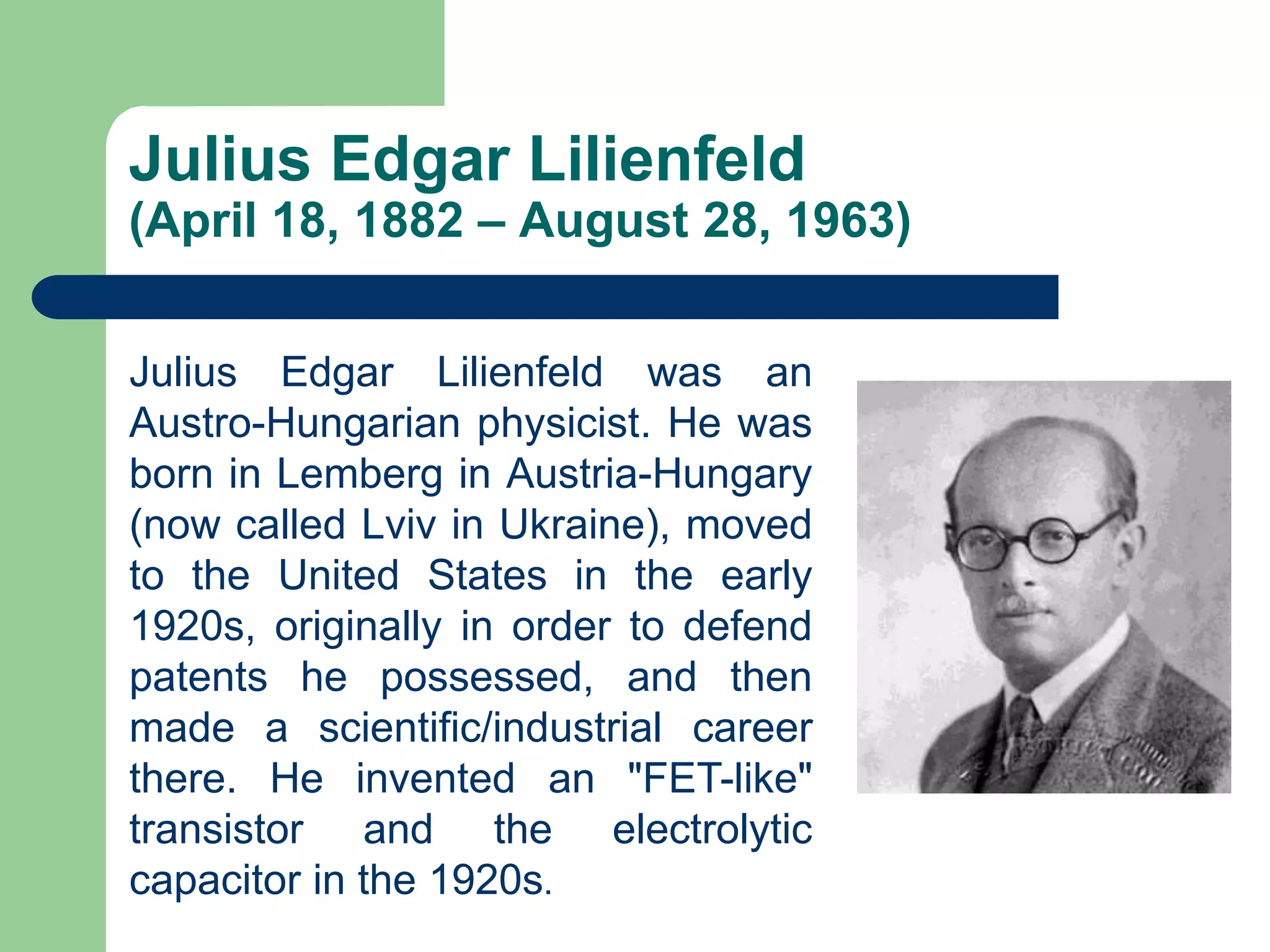
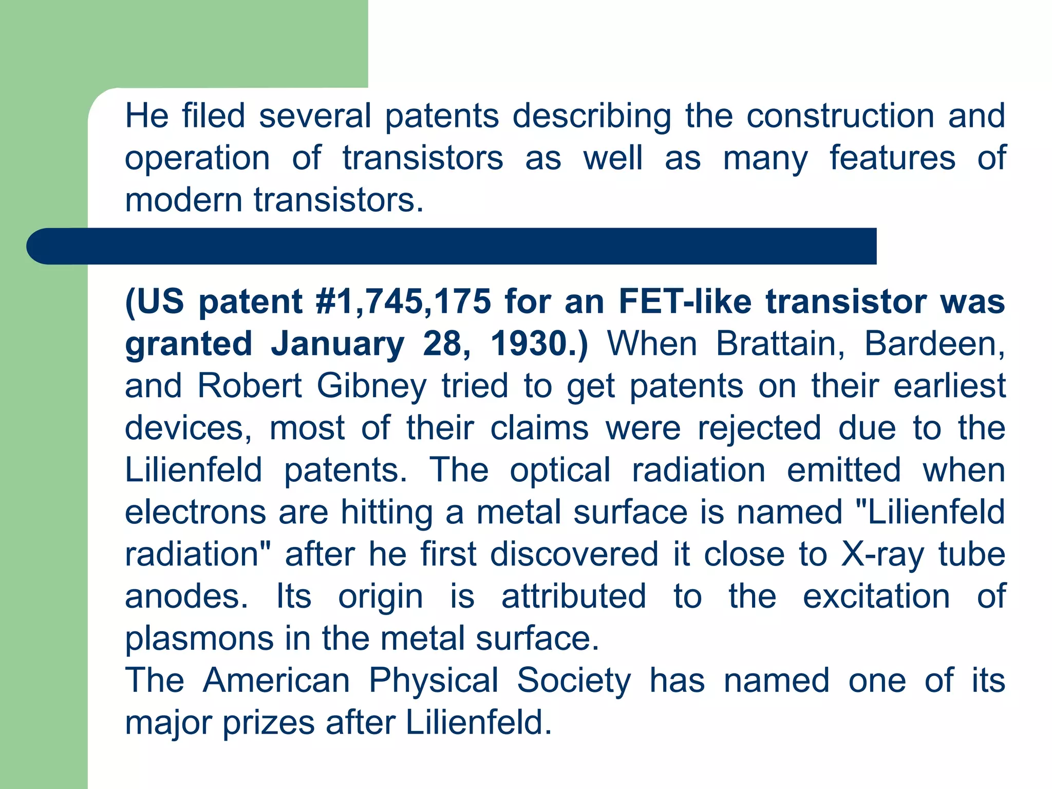
Biographical details of Julius Edgar Lilienfeld, a pioneer in transistor development and his contributions to the field.
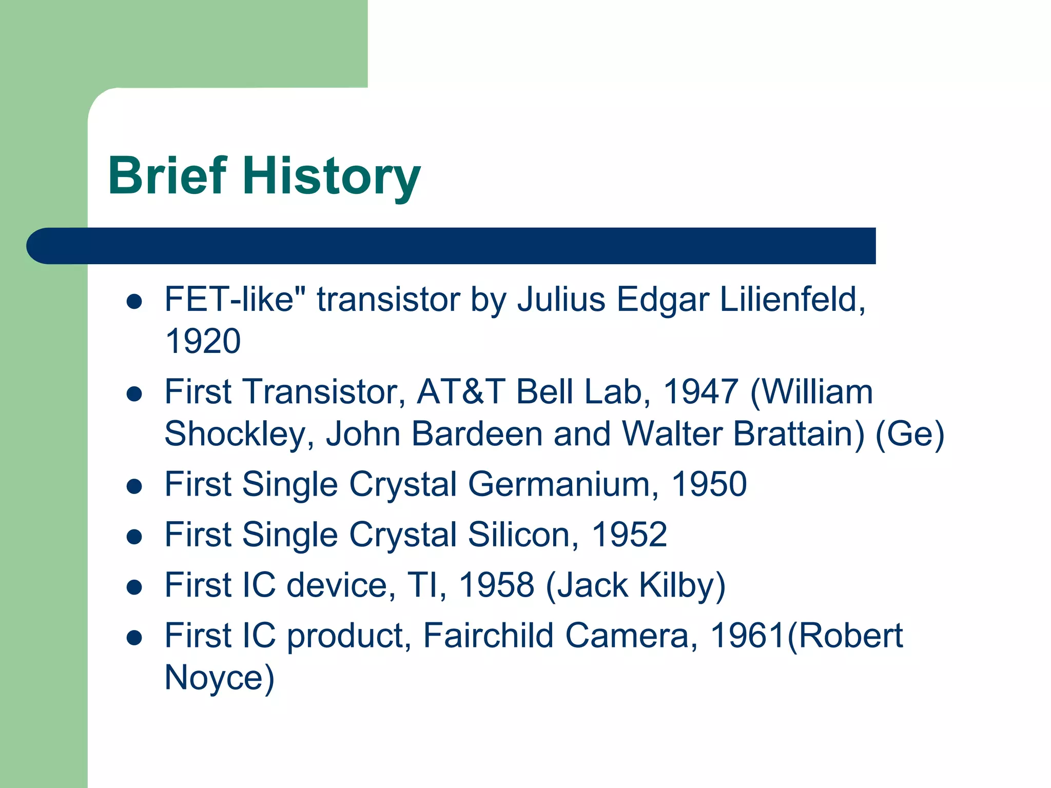
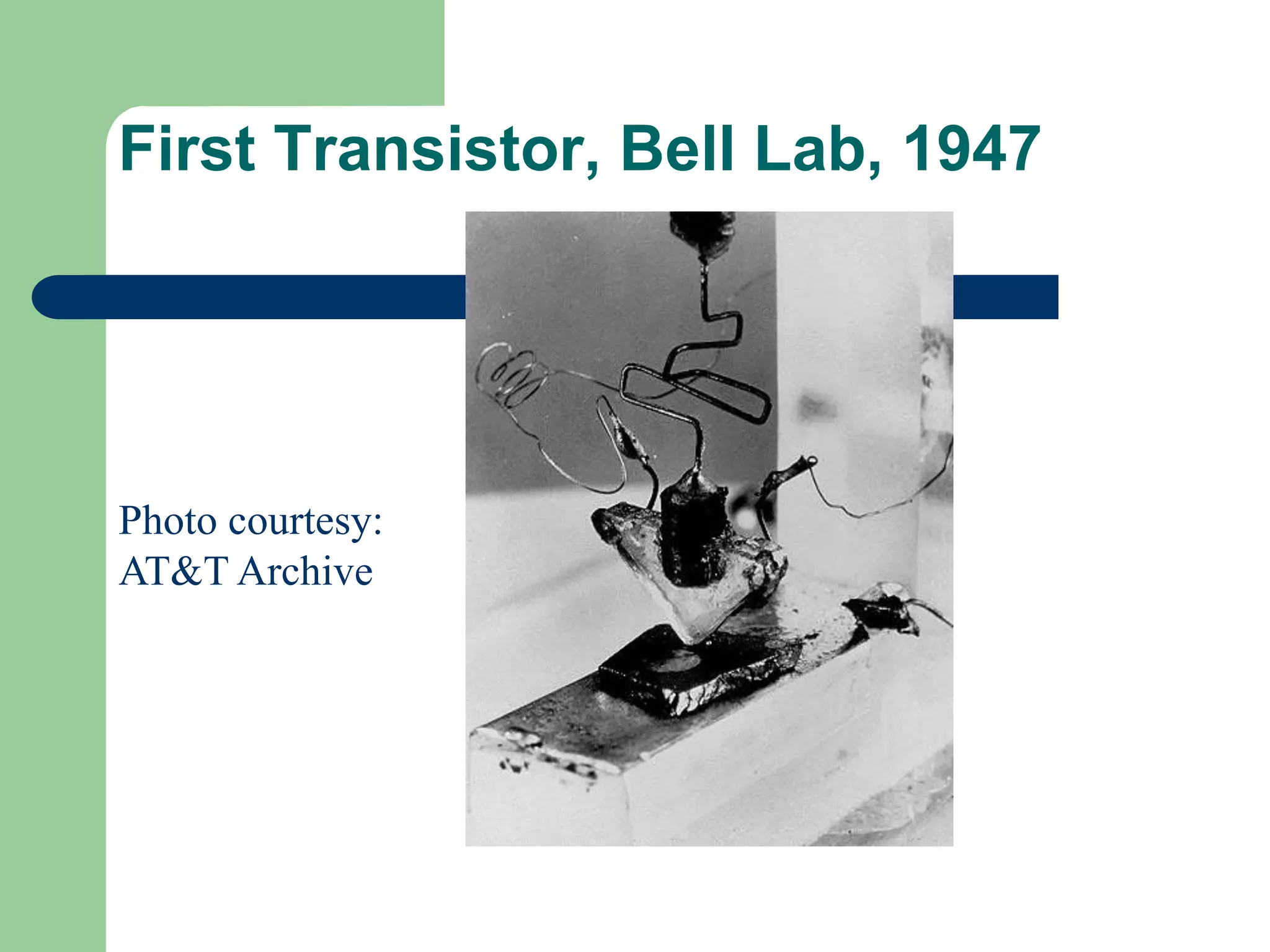
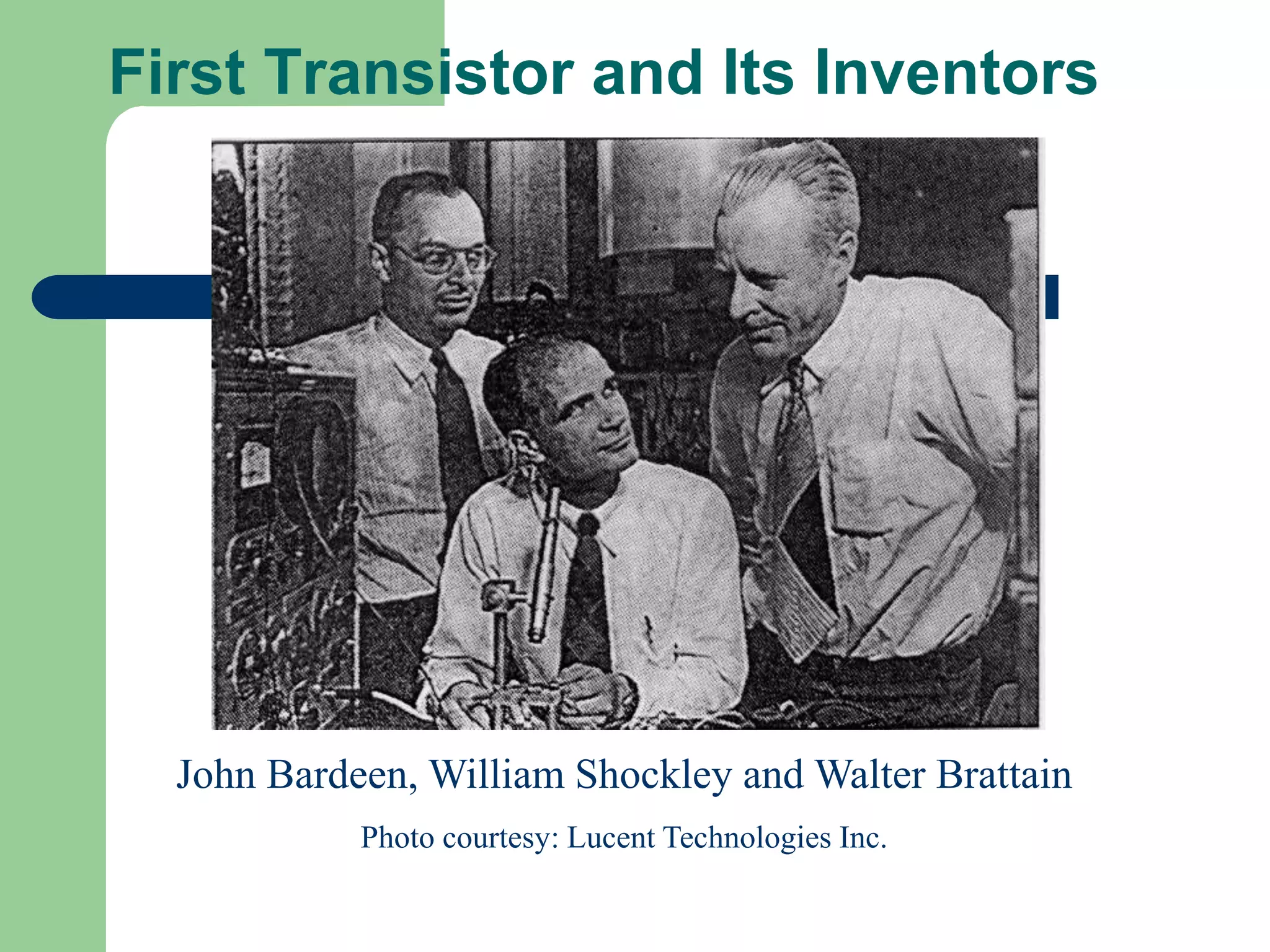
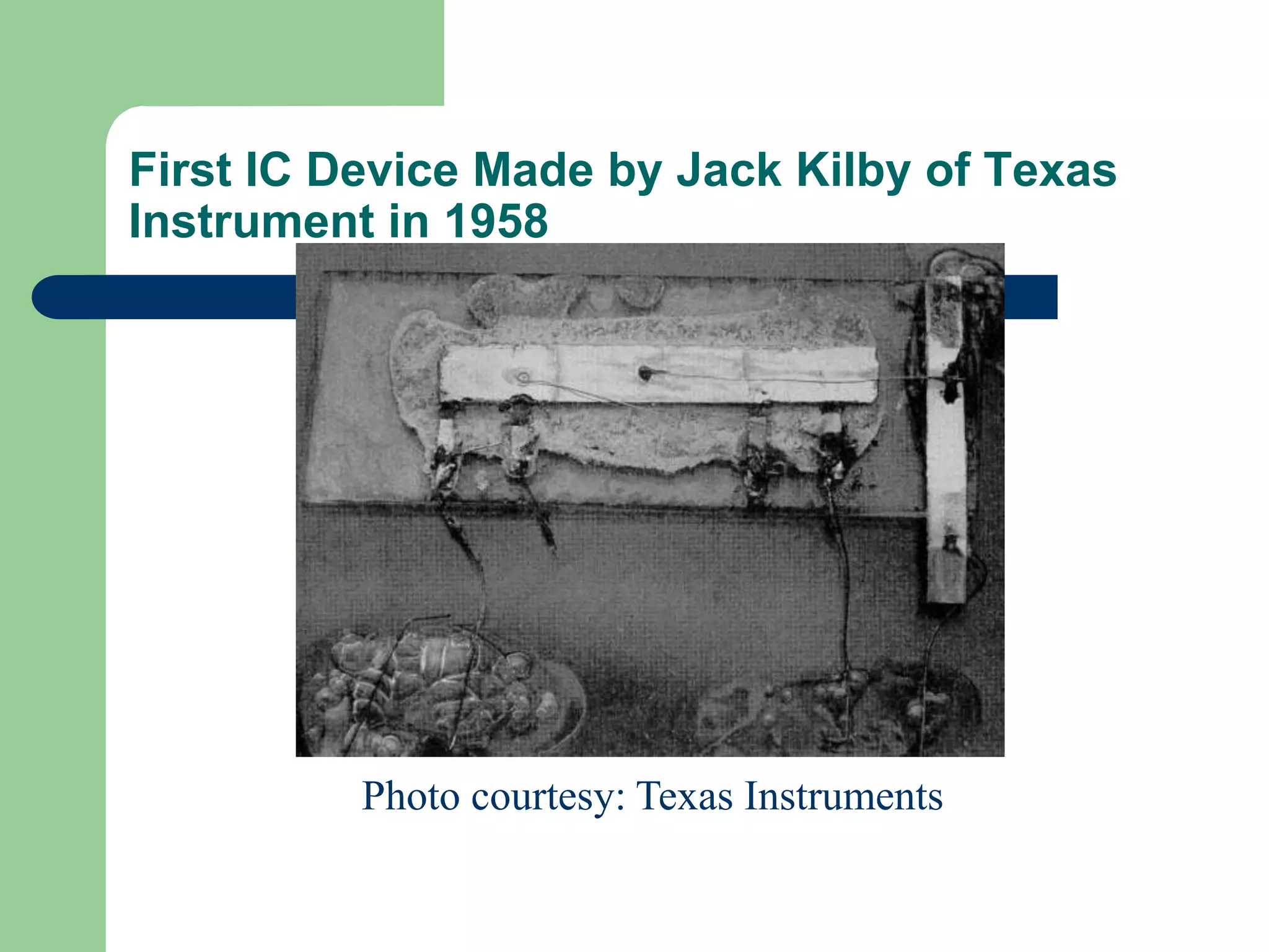
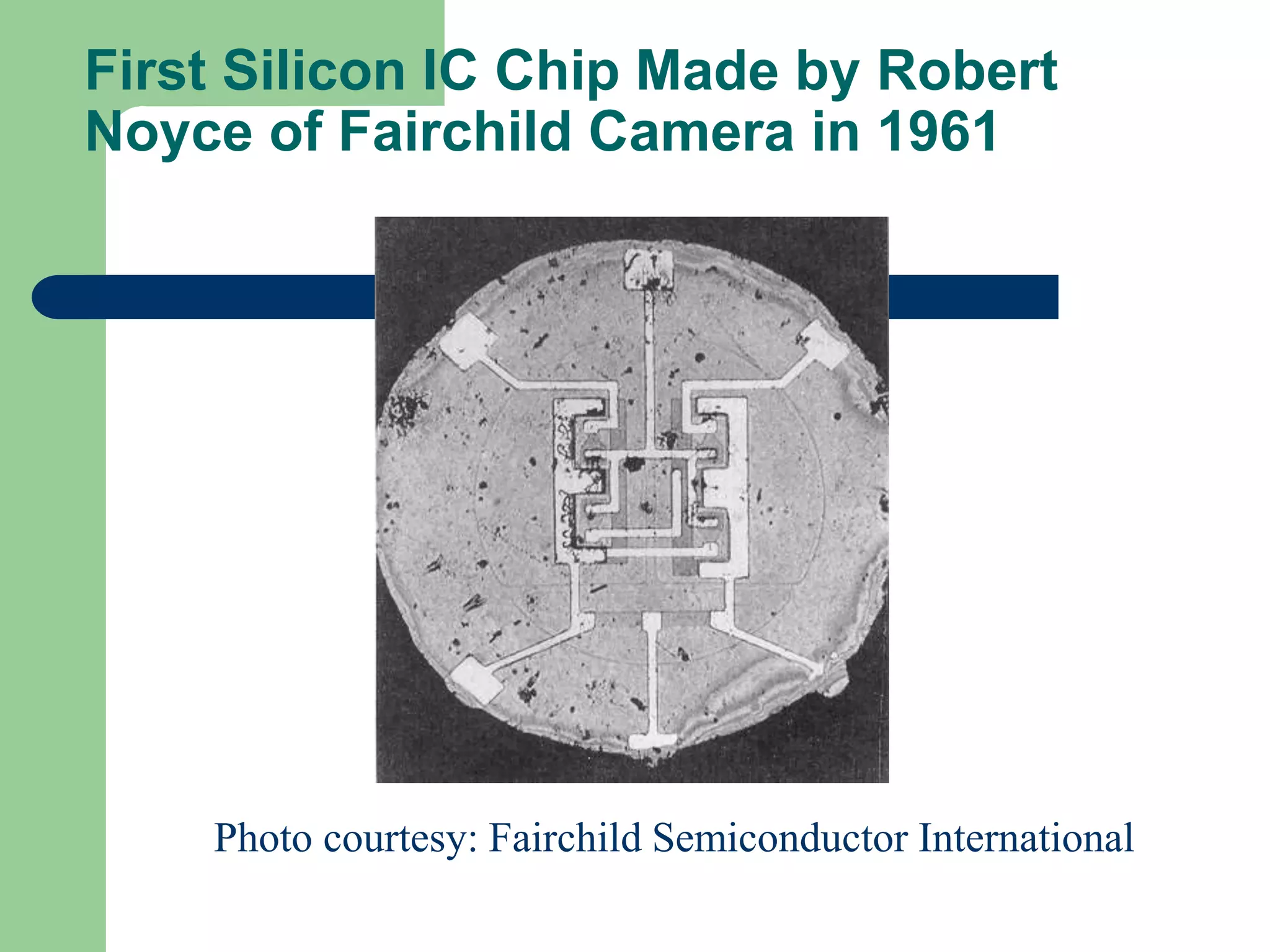
Timeline of key events in transistor history, from its invention by Lilienfeld to the development of the first IC devices.
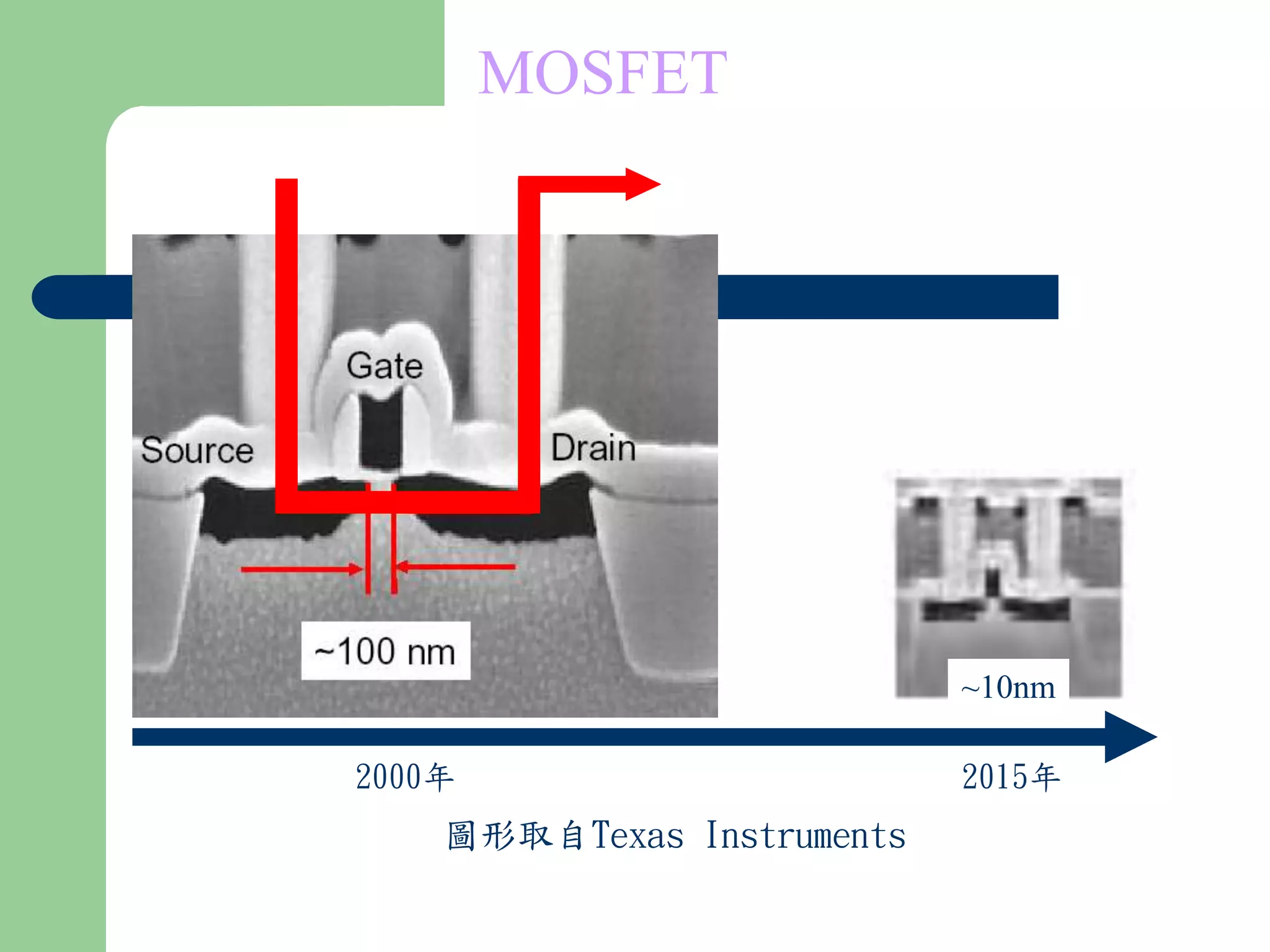
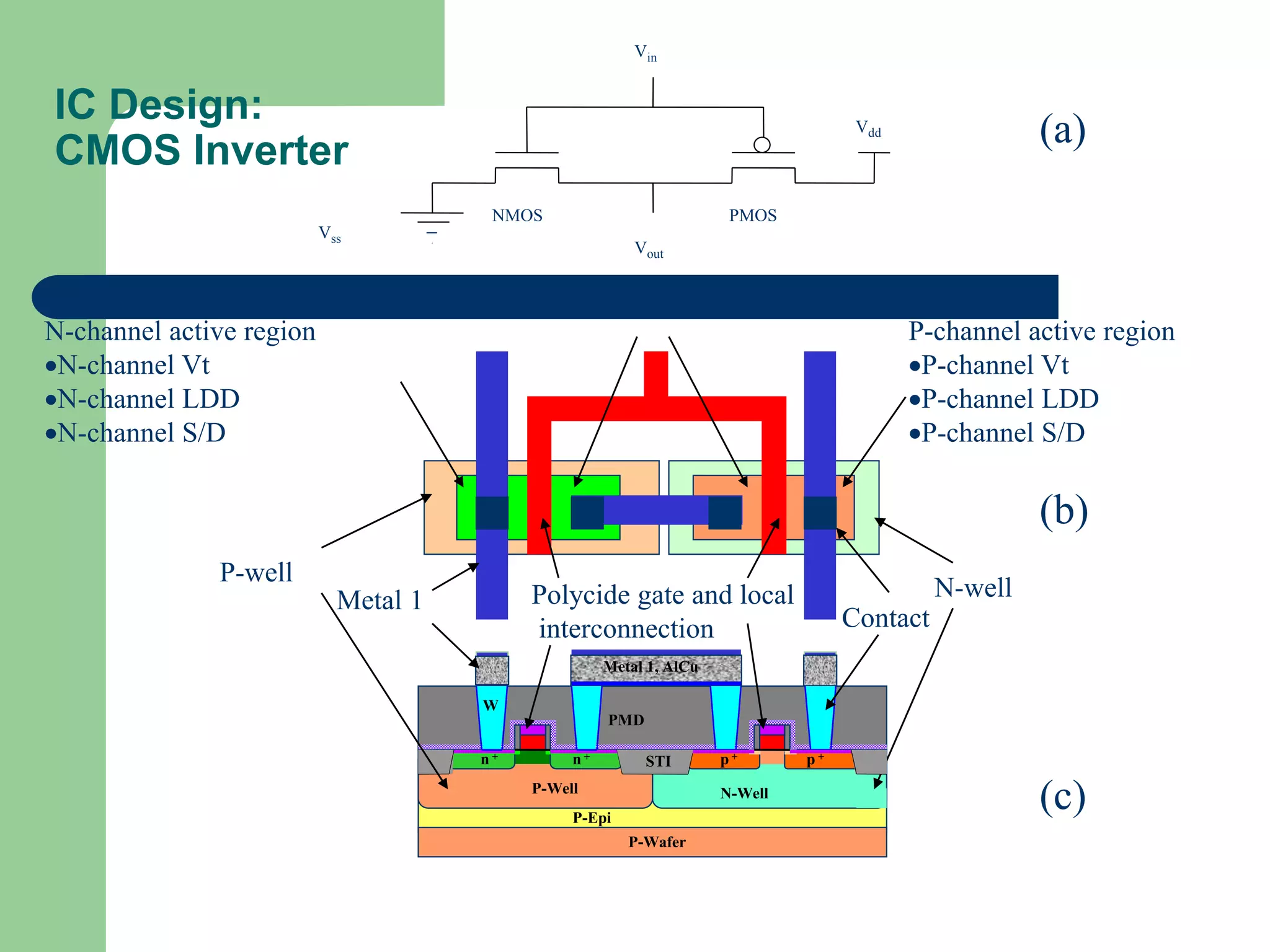
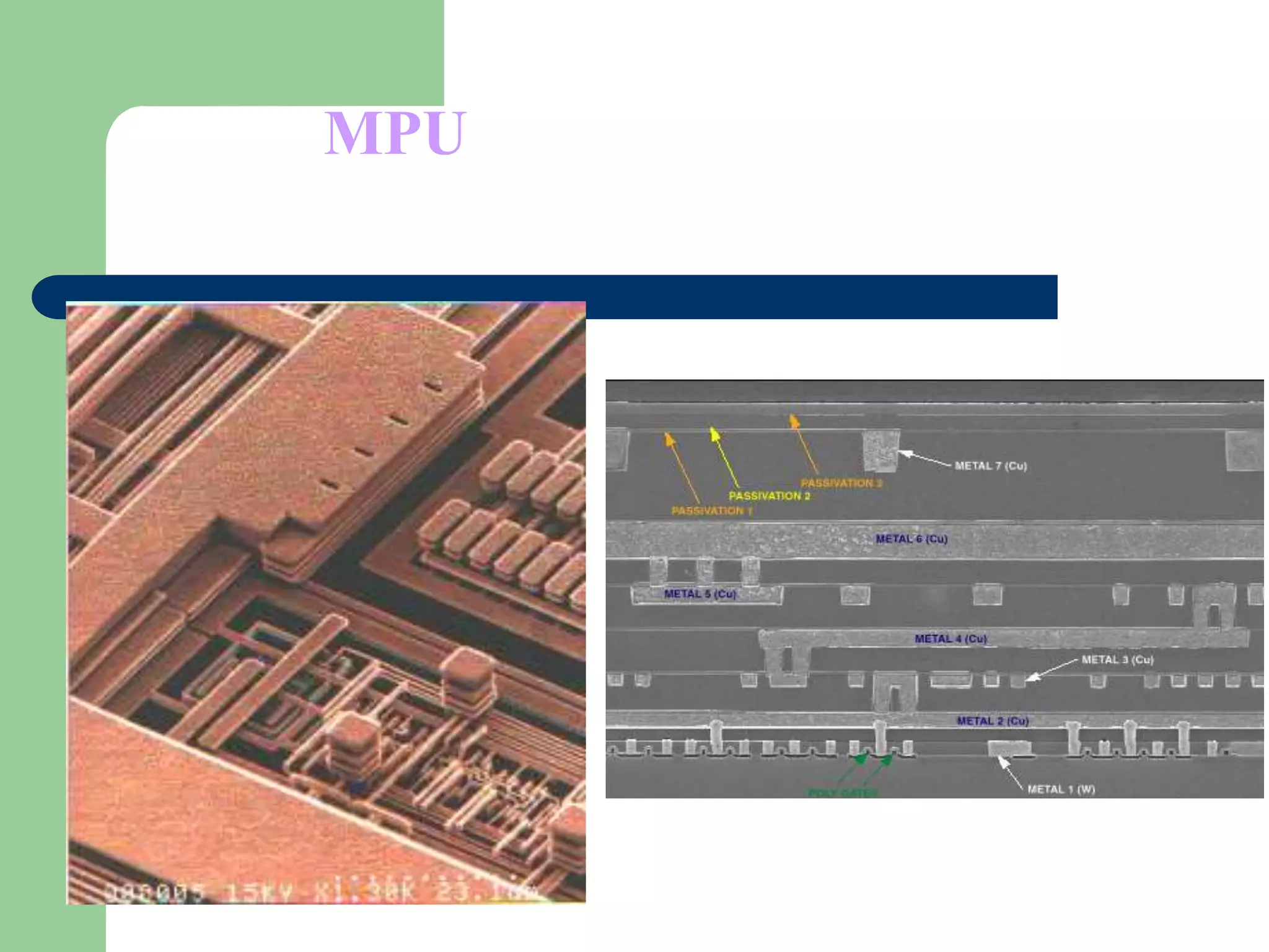
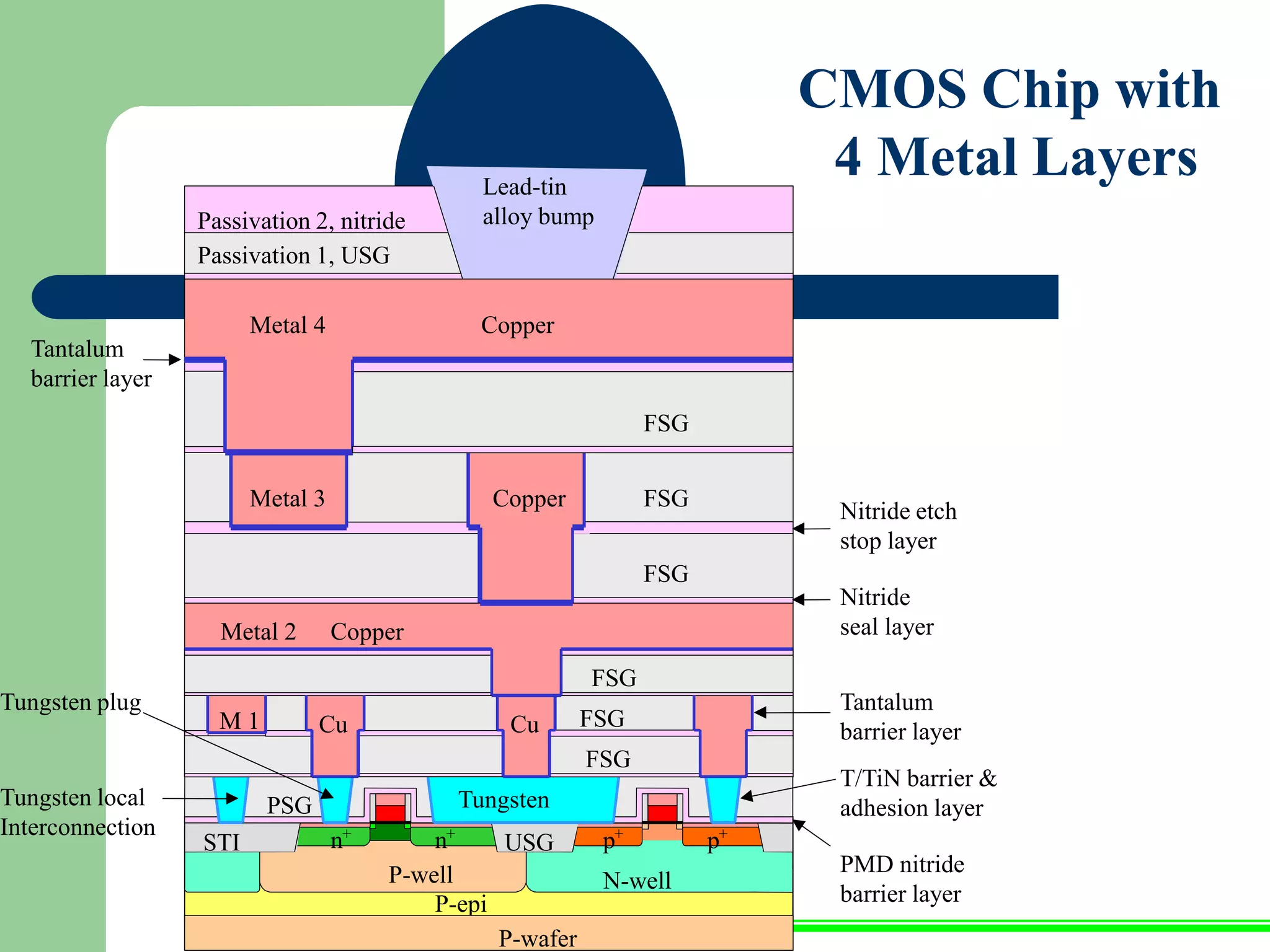
Introduction to MOSFET technology and detailed structures of CMOS chip design including multiple metal layers.