Downloaded 74 times
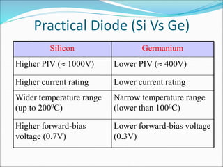

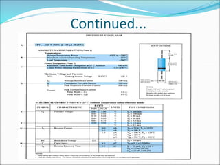
![Diode Specification Sheet
Data on specific semiconductor devices are normally provided by the manufacturer
in one of two forms. Most frequently, it is a very brief description limited to perhaps
one page. It includes:
1. The forward voltage VF (at a specified current and temperature)
2. The maximum forward current IF (at a specified temperature)
3. The reverse saturation current IR (at a specified voltage and temperature)
4. The reverse-voltage rating [PIV or PRV or V(BR), where BR comes from the term
“breakdown” (at a specified temperature)]
5. The maximum power dissipation level at a particular temperature
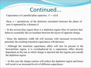
6. Capacitance levels
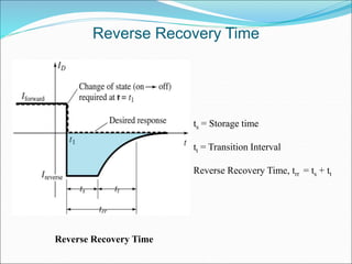
7. Reverse recovery time trr
8. Operating temperature range](https://image.slidesharecdn.com/semiconductordiodes-190815164811/85/Semiconductor-diodes-22-320.jpg)


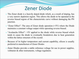
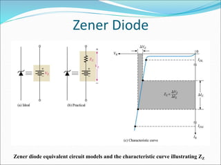
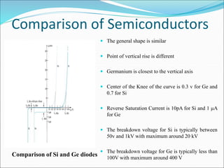
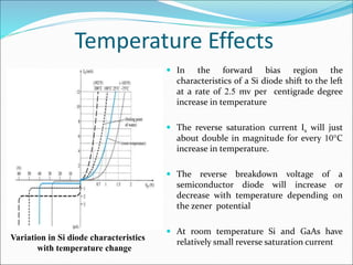
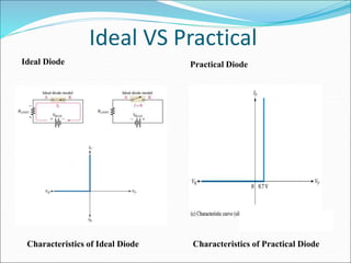
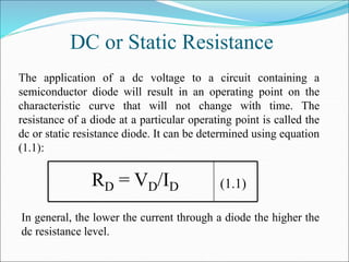
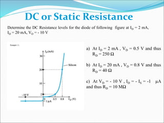
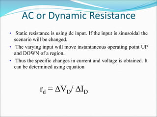
The document provides an overview of semiconductor diodes, particularly focusing on the characteristics and applications of zener diodes and their operational principles such as the zener effect and avalanche effect. It also compares silicon and germanium diodes, detailing their voltage ratings, resistance characteristics (dc and ac), and the impact of temperature on their performance. Additionally, the document discusses the light-emitting diode (LED), its electroluminescence process, and the specifications typically provided for semiconductor devices.


