Downloaded 16 times

![Synthesis
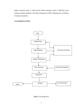
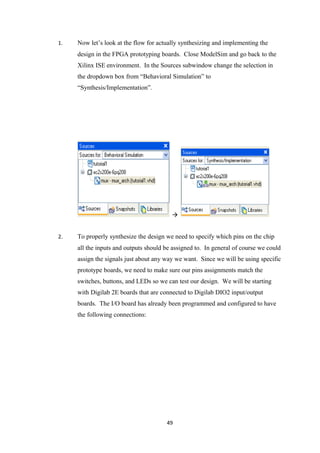
With the availability of design at the gate (switch) level, the logical design is
complete. The corresponding circuit hardware realization is carried out by a synthesis
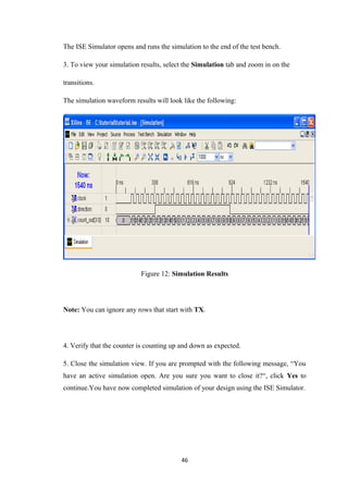
tool. Two common approaches are as follows:
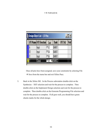
• The circuit is realized through an FPGA. The gate level design description is the
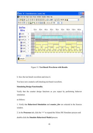
starting point for the synthesis here. The FPGA vendors provide an interface to the
synthesis tool. Through the interface the gate level design is realized as a final circuit.
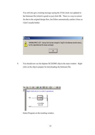
With many synthesis tools, one can directly use the design description at the data flow
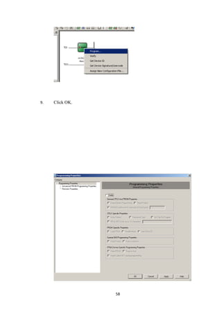
level itself to realize the final circuit through an FPGA. The FPGA route is attractive
for limited volume production or a fast development cycle.
• The circuit is realized as an ASIC. A typical ASIC vendor will have his own library
of basic components like elementary gates and flip-flops. Eventually the circuit is to
be realized by selecting such components and interconnecting them conforming to the
required design. This constitutes the physical design. Being an elaborate and costly
process, a physical design may call for an intermediate functional verification through
the FPGA route. The circuit realized through the FPGA is tested as a prototype. It
provides another opportunity for testing the design closer to the final circuit.
Physical Design
A fully tested and error-free design at the switch level can be the starting point
for a physical design [Baker & Boyce, Wolf]. It is to be realized as the final circuit
using (typically) a million components in the foundry’s library. The step-by-step
activities in the process are described briefly as follows:
• System partitioning: The design is partitioned into convenient compartments or
functional blocks. Often it would have been done at an earlier stage itself and the
software design prepared in terms of such blocks. Interconnection of the blocks is part
of the partition process.
• Floor planning: The positions of the partitioned blocks are planned and the blocks
are arranged accordingly. The procedure is analogous to the planning and
arrangement of domestic furniture in a residence. Blocks with I/O pins are kept close
to the periphery; those which interact frequently or through a large number of
interconnections are kept close together, and so on. Partitioning and floor planning
may have to be carried out and refined iteratively to yield best results.
6](https://image.slidesharecdn.com/highbitratemul-130416071536-phpapp02/85/High-bit-rate_mul-6-320.jpg)
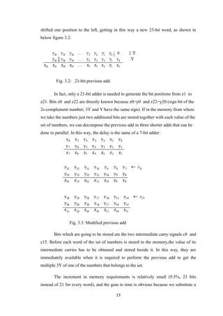
![Fig. 3.5: Partial products multiplexer.
c) The partial product length is two bits longer than the multiplicand length, giving
23-bit length partial products.
d) The number of partial products entering the Wallace tree structure is 8: 7 coming
from the multiplier recoded digits plus another partial product due to the compensation
bits of the 2scomplement multiplication algorithm which cannot be included in any of
the other 7 words.
e) The best structure for the reduction of 8 partial products applies only 4-2
compressors [7] (instead of the conventional full adders) .
The Wallace tree has the following scheme:
Fig. 8: Wallace reduction tree.
with an equivalent delay of 6 logic gates.
15](https://image.slidesharecdn.com/highbitratemul-130416071536-phpapp02/85/High-bit-rate_mul-15-320.jpg)
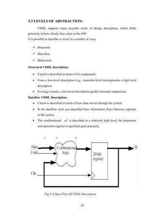
![• The behavior of the system over the time is defined by registers.
• There are no build-in registers in VHDL-language.
-Either lowers level description.
-Or behavioral description of sequential elements is needed.
• The lower level descriptions must be created or obtained.
• If their is no 3rd party models for registers => you must write the behavioral
description of registers.
• The behavioral description can be provided in the form of
subprograms(functions or procedures).
Behavioral VHDL Description
• Circuit is described in terms of its operation over time.
• Representation might include, e.g., state diagrams ,timing diagrams and
algorithmic descriptions.
• The concept of time may be expressed precisely using delays(e.g., A<=B after
10ns).
• If no actual delay is used, order of sequential operations is defined.
• In the lower level of abstraction (e.g., RTL) synthesis tools ignore detailed
timing specifications.
• The actual timing results depend on implementation technology and efficiency
of synthesis tools.
• There are few tools for behavioral synthesis.
General format:
Process [(sensitivity list)]
Process_declarative_part
Begin
Process_statements
[wait_statement]
End process
26](https://image.slidesharecdn.com/highbitratemul-130416071536-phpapp02/85/High-bit-rate_mul-26-320.jpg)

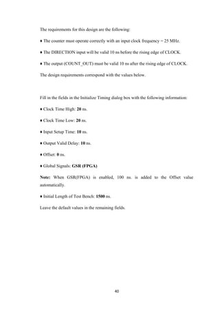
![Use a simple counter code example from the ISE Language Templates and customize
it for the counter design.
1. Place the cursor on the line below the output [3:0] COUNT_OUT; statement.
2. Open the Language Templates by selecting Edit → Language Templates…
Note: You can tile the Language Templates and the counter file by selecting Window
→ Tile Vertically to make them both visible.
3. Using the “+” symbol, browse to the following code example:
Verilog → Synthesis Constructs → Coding Examples → Counter → Binary →
Up/Down Counters → Simple Counter
4. With Simple Counter selected, select Edit → Use in File, or select the Use
Template in File toolbar button. This step copies the template into the counter source
file.
5. Close the Language Templates.
Final Editing of the Verilog Source
1. To declare and initialize the register that stores the counter value, modify the
declaration statement in the first line of the template as follows:
replace: reg [<upper>:0] <reg_name>;
with: reg [3:0] count_int = 0;
2. Customize the template for the counter design by replacing the port and signal
name
placeholders with the actual ones as follows:
♦ replace all occurrences of <clock> with CLOCK
♦ replace all occurrences of <up_down> with DIRECTION
♦ replace all occurrences of <reg_name> with count_int
37](https://image.slidesharecdn.com/highbitratemul-130416071536-phpapp02/85/High-bit-rate_mul-37-320.jpg)
![3. Add the following line just above the endmodule statement to assign the register
value to the output port:
assign COUNT_OUT = count_int;
4. Save the file by selecting File → Save.
When you are finished, the code for the counter will look like the following:
module counter(CLOCK, DIRECTION, COUNT_OUT);
input CLOCK;
input DIRECTION;
output [3:0] COUNT_OUT;
reg [3:0] count_int = 0;
always @(posedge CLOCK)
if (DIRECTION)
count_int <= count_int + 1;
else
count_int <= count_int - 1;
assign COUNT_OUT = count_int;
endmodule
You have now created the Verilog source for the tutorial project.
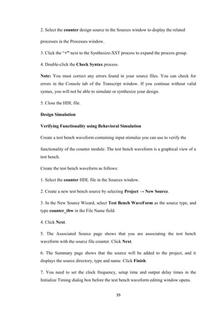
Checking the Syntax of the New Counter Module
When the source files are complete, check the syntax of the design to find errors and
typos.
1. Verify that Synthesis/Implementation is selected from the drop-down list in the
Sources window.
38](https://image.slidesharecdn.com/highbitratemul-130416071536-phpapp02/85/High-bit-rate_mul-38-320.jpg)
![REFERENCE
[1] Dong-Wook Kim, Young-Ho Seo, “A New VLSI Architecture of Parallel
Multiplier-Accumulator based on Radix-2 Modified Booth Algorithm”, Very Large
Scale Integration (VLSI) Systems, IEEE Transactions, vol.18, pp.: 201-208, 04 Feb.
2010
[2] Prasanna Raj P, Rao, Ravi, “VLSI Design and Analysis of Multipliers for Low
Power”, Intelligent Information Hiding and Multimedia Signal Processing, Fifth
International Conference, pp.: 1354-1357, Sept. 2009
60](https://image.slidesharecdn.com/highbitratemul-130416071536-phpapp02/85/High-bit-rate_mul-60-320.jpg)
![[3] Lakshmanan, Masuri Othman and Mohamad Alauddin Mohd.Ali, “High
Performance Parallel Multiplier using Wallace-Booth Algorithm”, Semiconductor
Electronics, IEEE International Conference , pp.: 433- 436, Dec. 2002.
[4] Jan M Rabaey, “Digital Integrated Circuits, A Design Perspective”, Prentice Hall,
Dec.1995
[5] Louis P. Rubinfield, “A Proof of the Modified Booth's Algorithm for
Multiplication”, Computers, IEEE Transactions,vol.24, pp.: 1014-1015, Oct. 1975
[6] Rajendra Katti, “A Modified Booth Algorithm for High Radix Fixedpoint
Multiplication”, Very Large Scale Integration (VLSI) Systems, IEEE Transactions,
vol. 2, pp.: 522-524, Dec. 1994.
7] C. S. Wallace, “A Suggestion for a Fast Multiplier”, Electronic Computers, IEEE
Transactions, vol.13, Page(s): 14-17, Feb. 1964
[8] Hussin R et al , “An Efficient Modified Booth Multiplier Architecture”, IEEE
International Conference, pp.:1-4, 2008.
61](https://image.slidesharecdn.com/highbitratemul-130416071536-phpapp02/85/High-bit-rate_mul-61-320.jpg)

The document discusses VLSI design and a high-speed parallel multiplier project. It begins with an introduction to VLSI design including its history and various integrations from SSI to VLSI. It then provides an overview and motivation for the multiplier project. The project aims to implement efficient high-speed multiplication using Booth encoding, Wallace tree adders, and carry look-ahead adders to reduce the number of partial products and accelerate their accumulation. The document outlines the organization of the project report and chapters on Booth algorithms, Wallace trees, and carry look-ahead addition.