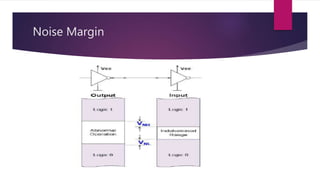
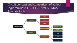
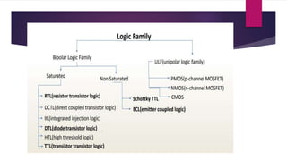
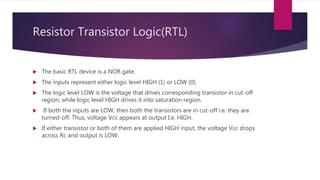
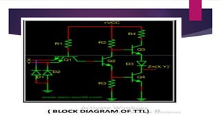
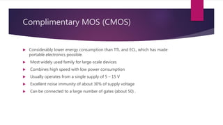
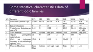
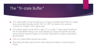
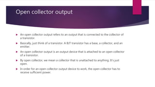
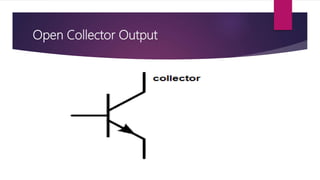
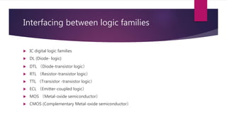
LOGIC FAMILIES(UNIT 4)
BY:SURBHI SAROHA
SYLLABUS
 Diode
 BJT & MOS as switching element.
 Concept of transfer characteristics.
 Input characteristic and output characteristics of logic gates.
 Fan- in
 Fan-out
 Noise margin
 Circuit concept and comparison of various logic families : TTL,IIL,ECL,NMOS,CMOS
Tri-state logic
SYLLABUS
 Open collector output
 Interfacing between logic families
 Packing density
 Power consumption & gate delay.
Diode
 The anode which is the positive terminal of a diode is represented with A and
the cathode, which is the negative terminal is represented with K.
 To know the anode and cathode of a practical diode, a fine line is drawn on the
diode which means cathode, while the other end represents anode.
Diode(Cont….)
 Diodes are used to protect circuits by limiting the voltage and to also transform
AC into DC.
 Semiconductors like silicon and germanium are used to make the most of the
diodes.
 Even though they transmit current in a single direction, the way with which they
transmit differs.
 There are different kinds of diodes and each type has its own applications.
BJT & MOS as switching element
 Bipolar junction transistors (Also known as BJTs) can be used as an amplifier,
filter, rectifier, oscillator, or even a switch, which we cover an example in the
first section.
 The transistor will operate as an amplifier or other linear circuit if the transistor is
biased into the linear region.
 The transistor can be used as a switch if biased in the saturation and cut-off
regions.
 This allows current to flow (or not) in other parts of a circuit.
 Because a transistor’s collector current is proportionally limited by its base current,
it can be used as a sort of current-controlled switch.
BJT & MOS as switching element(Cont..)
 A relatively small flow of electrons sent through the base of the transistor has the
ability to exert control over a much larger flow of electrons through the collector.
 Bipolar junction transistor (BJT) has three terminals and two junctions.
 The function of the transistor is to amplify the signal.
 The three terminals of BJT are base, emitter and collector.
 BJT is either a PNP transistor or NPN transistor based on the doping type of the
three terminals.
 Using the transistor as a switch is the simplest application of transistors.
How does a BJT act as a switch?
 A transistor has three modes: active region, cut off region and the saturation
region.
 The transistor acts as a switch in the cut-off mode and the saturation mode.
 The transistor is fully off in the cutoff region and fully on the saturation region.
 A transistor can also be used as a switch since a small electric current flowing
through one part of it can cause larger current flow through the other part of the
transistor.
MOS as a Switch
 MOSFETs exhibit three regions of operation viz., Cut-off, Linear or Ohmic and
Saturation.
 Among these, when MOSFETs are to be used as amplifiers, they are required to be
operated in their ohmic region wherein the current through the device increases with
an increase in the applied voltage.
 On the other hand, when the MOSFETs are required to function as switches, they
should be biased in such a way that they alter between cut-off and saturation states.
 This is because, in cut-off region, there is no current flow through the device while in
saturation region there will be a constant amount of current flowing through the
device, just mimicking the behaviour of an open and closed switch, respectively.
 This functionality of MOSFETs is exploited in many electronic circuits as they offer
higher switching rates when compared to BJTs (bipolar junction transistors).
MOS(Cont….)
 The MOSFET (Metal Oxide Semiconductor Field Effect Transistor) transistor is a
semiconductor device that is widely used for switching purposes and for the
amplification of electronic signals in electronic devices.
 A MOSFET is either a core or integrated circuit where it is designed and
fabricated in a single chip because the device is available in very small sizes.
 In general, The body of the MOSFET is in connection with the source terminal
thus forming a three-terminal device such as a field-effect transistor.
 MOSFET is generally considered as a transistor and employed in both the
analog and digital circuits.
A MOSFET is a four-terminal device having source(S), gate (G), drain (D) and body
(B) terminals.
Concept of transfer characteristics
 The transfer characteristics of a system is defined to be the pseudo-static
relationship between the input and output variable.
 If the system is a voltage-in, voltage-out system we would term this pseudo-static
relationship the dc transfer characteristics.
 A system with an input XIN and an output XOUT .
 In electrical systems the input and output quantities, typically termed signals, are
often dependent on a single additional input variable, time.
 In this case the input and output signals would time-dependent voltages or
currents.
Input characteristic and output
characteristics of logic gates
 Propagation delay
 It is the time interval between the application of the input pulse and the
occurrence of the output. It is an important characteristic of the digital logic
family. If the propagation delay is less, then the speed at which the IC operates
will be faster.
 Let THL is the propagation delay when the output changes from logic 0 to 1 and
TLH is the delay when the output changes from logic 1 to 0. The maximum value of
THL and TLH is considered as the propagation delay for that logic gate.
Fan in and Fan out
 Fan-in refers to the number of inputs in a digital logic gate family. For the
example given in the figure below, the EX-OR gate has three inputs. So fan-in
for the given EX-OR gate is 3.
Fan-out
 Fan-out refers to the number of inputs that is driven by the output of another
logic gates. For example, the following circuit has an EX-OR gate, which drives 4
NOT gates. So fan-out of EX-OR gate is 4.
Fan-out
 •The maximum number of digital input that the output of a single logic gate can
feed and the gate must be same logic family.
 • Fan Out is calculated from the amount of current available in the output of a
gate and the amount of current needed in each input of the connecting gate.
 •It is specified by manufacturer and is provided in the data sheet.
 •Exceeding the specified maximum load may cause a malfunction because the
circuit will not be able supply the demanded power.
What is Noise?
 It is an unwanted signal that is superimposed on the normal operating signal.
Noise may be due to various factors like operating environment, radiations, stray
electrical and magnetic fields.
 In digital logic circuits, the binary values 0 and 1 represent the LOW and HIGH
voltage levels. Due to the interference of the noises, the voltage levels may
increase or decrease. This may lead to the wrong operation of the device.
 The noise immunity is the ability of the logic device to tolerate the noise without
causing spurious change to the output voltage. Noise margin allows the logic
device to function properly within the specified limits.
Noise Margin
 •Noise is present in all real systems.
 This adds random fluctuations to voltages representing logic levels.
 •Hence, the voltage ranges defining the logic levels are more tightly constrained
at the output of a gate than at the input.
 • Small amounts of noise will not affect the circuit.
 The maximum noise voltage that can be tolerated by a circuit is termed its noise
immunity (noise Margin).
Noise Margin
Circuit concept and comparison of various
logic families : TTL,IIL,ECL,NMOS,CMOS
Tri-state logic
Resistor Transistor Logic(RTL)
 The basic RTL device is a NOR gate.
 The inputs represent either logic level HIGH (1) or LOW (0).
 The logic level LOW is the voltage that drives corresponding transistor in cut-off
region, while logic level HIGH drives it into saturation region.
 If both the inputs are LOW, then both the transistors are in cut-off i.e. they are
turned-off. Thus, voltage Vcc appears at output I.e. HIGH.
 If either transistor or both of them are applied HIGH input, the voltage Vcc drops
across Rc and output is LOW.
Diode Transistor Logic
 The diode-transistor logic, also termed as DTL, replaced RTL family because of greater
fan-out capability and more noise margin.
 DTL circuits mainly consists of diodes and transistors that comprises DTL devices.
 The basic DTL device is a NAND gate.
 Two inputs to the gate are applied through diodes viz. D1, D2 .
 The diode will conduct only when corresponding input is LOW.
 If any of the diode is conducting i.e. when at least one input is LOW, the voltage at
output keeps transistor T in cut-off and subsequently, output of transistor is HIGH.
 If all inputs are HIGH, all diodes are non-conducting, transistor T is in saturation, and its
output is LOW.
Diode Transistor Logic
 Due to number of diodes used in this circuit, the speed of the circuit is
significantly low.
 Hence this family of logic gates is modified to transistor-transistor logic i.e. TTL
family which has been discussed on next slide.
Transistor Transistor Logic
 TTL family is a modification to the DTL.
 It has come to existence so as to overcome the speed limitations of DTL family.
 The basic gate of this family is TTL NAND gate.
 Q3 is cutoff (act like a high RC ) when output transistor Q4 is saturated and Q3 is
saturated (act like a low RC ) when output transistor Q4 is cutoff .
 Thus one transistor is ON at one time.
 The combination of Q3 and Q4 is called TOTEM POLE arrangement.
 Q1 is called input transistor, which is multi emitter transistor, that drive transistor Q2
which is used to control Q3 and Q4.
 Diode D1 and D2 are used to protect Q1 from unwanted negative voltages and diode
D3 ensures when Q4 is ON, Q3 is OFF.
Transistor Transistor Logic
 The output impedance is asymmetrical between the high and low state, making
them unsuitable for driving transmission lines.
 This drawback is usually overcome by buffering the outputs with special line-
driver devices where signals need to be sent through cables.
 ECL, by virtue of its symmetric low-impedance output structure, does not have this
drawback.
Complimentary MOS (CMOS)
 Considerably lower energy consumption than TTL and ECL, which has made
portable electronics possible.
 Most widely used family for large-scale devices
 Combines high speed with low power consumption
 Usually operates from a single supply of 5 – 15 V
 Excellent noise immunity of about 30% of supply voltage
 Can be connected to a large number of gates (about 50) .
Some statistical characteristics data of
different logic families
The “Tri-state Buffer”
 A Tri-state Buffer can be thought of as an input controlled switch with an output
that can be electronically turned “ON” or “OFF” by means of an external
“Control” or “Enable” ( EN ) signal input.
 This control signal can be either a logic “0” or a logic “1” type signal resulting in
the Tri-state Buffer being in one state allowing its output to operate normally
producing the required output or in another state were its output is blocked or
disconnected.
 Then a tri-state buffer requires two inputs.
 One being the data input and the other being the enable or control input as
shown.
Tri-state Buffer Switch Equivalent
Open collector output
 An open collector output refers to an output that is connected to the collector of
a transistor.
 Basically, just think of a transistor. A BJT transistor has a base, a collector, and an
emitter.
 An open collector output is an output device that is attached to an open collector
of a transistor.
 By open collector, we mean a collector that is unattached to anything. It's just
open.
 In order for an open collector output device to work, the open collector has to
receive sufficient power.
Open Collector Output
Interfacing between logic families
 IC digital logic families
 DL (Diode- logic)
 DTL (Diode-transistor logic)
 RTL (Resistor-transistor logic)
 TTL (Transistor -transistor logic)
 ECL (Emitter-coupled logic)
 MOS (Metal-oxide semiconductor)
 CMOS (Complementary Metal-oxide semiconductor)
Voltage-Related Interfacing Problems
 In some interfacing situations, a HIGH output pin may produce a voltage that is
too low to be recognized as a HIGH by the input pin it’s connected to.
 The solution in such cases is to use a pull-up resistor
 Example: TTL to CMOS
 A TTL HIGH output may be as low as 2.4 V.
 But a CMOS input expects HIGHs to be at least 3.33 V.
TTL to CMOS
Packing density
 TTL is Saturated Logic, ECL is Maximum power consumption, NMOS is Highest
packing density, CMOS is Least power consumption.
Power consumption & gate delay
 Propagation delay of a gate is not the same thing as rise or fall time for an
individual transistor.
 To propagate through an IC a signal may have to pass through several transistors
and may pass through different transistor paths depending on the kind of input
(data, select, enable, etc) being asserted.
 A small amount of delay in signal transmission is unavoidable because of the finite
speed of light, which travels one foot per nanosecond (signals move in wire at
nearly the speed of light).
 But most delay in switching circuits is due to the time it takes charges stored in
one place to move to another.
Power consumption & gate delay(Cont…)
 The removal of stored charge from a capacitor through a resistance to "ground"
takes time, in the same way that emptying a bathtub through the drain takes time.
 Electronic switches are made of transistors.
 Consider the input side of a common-emitter transistor circuit, and the case of
turning it off-charge caught in the base region must be removed before the flow
of current from collector to emitter is stopped.
 To a certain approximation the base-emitter junction of a transistor acts like a
capacitor.
Thank you

Logic families(unit 4)

  • 1.
  • 2.
    SYLLABUS  Diode  BJT& MOS as switching element.  Concept of transfer characteristics.  Input characteristic and output characteristics of logic gates.  Fan- in  Fan-out  Noise margin  Circuit concept and comparison of various logic families : TTL,IIL,ECL,NMOS,CMOS Tri-state logic
  • 3.
    SYLLABUS  Open collectoroutput  Interfacing between logic families  Packing density  Power consumption & gate delay.
  • 4.
    Diode  The anodewhich is the positive terminal of a diode is represented with A and the cathode, which is the negative terminal is represented with K.  To know the anode and cathode of a practical diode, a fine line is drawn on the diode which means cathode, while the other end represents anode.
  • 5.
    Diode(Cont….)  Diodes areused to protect circuits by limiting the voltage and to also transform AC into DC.  Semiconductors like silicon and germanium are used to make the most of the diodes.  Even though they transmit current in a single direction, the way with which they transmit differs.  There are different kinds of diodes and each type has its own applications.
  • 6.
    BJT & MOSas switching element  Bipolar junction transistors (Also known as BJTs) can be used as an amplifier, filter, rectifier, oscillator, or even a switch, which we cover an example in the first section.  The transistor will operate as an amplifier or other linear circuit if the transistor is biased into the linear region.  The transistor can be used as a switch if biased in the saturation and cut-off regions.  This allows current to flow (or not) in other parts of a circuit.  Because a transistor’s collector current is proportionally limited by its base current, it can be used as a sort of current-controlled switch.
  • 7.
    BJT & MOSas switching element(Cont..)  A relatively small flow of electrons sent through the base of the transistor has the ability to exert control over a much larger flow of electrons through the collector.  Bipolar junction transistor (BJT) has three terminals and two junctions.  The function of the transistor is to amplify the signal.  The three terminals of BJT are base, emitter and collector.  BJT is either a PNP transistor or NPN transistor based on the doping type of the three terminals.  Using the transistor as a switch is the simplest application of transistors.
  • 8.
    How does aBJT act as a switch?  A transistor has three modes: active region, cut off region and the saturation region.  The transistor acts as a switch in the cut-off mode and the saturation mode.  The transistor is fully off in the cutoff region and fully on the saturation region.  A transistor can also be used as a switch since a small electric current flowing through one part of it can cause larger current flow through the other part of the transistor.
  • 9.
    MOS as aSwitch  MOSFETs exhibit three regions of operation viz., Cut-off, Linear or Ohmic and Saturation.  Among these, when MOSFETs are to be used as amplifiers, they are required to be operated in their ohmic region wherein the current through the device increases with an increase in the applied voltage.  On the other hand, when the MOSFETs are required to function as switches, they should be biased in such a way that they alter between cut-off and saturation states.  This is because, in cut-off region, there is no current flow through the device while in saturation region there will be a constant amount of current flowing through the device, just mimicking the behaviour of an open and closed switch, respectively.  This functionality of MOSFETs is exploited in many electronic circuits as they offer higher switching rates when compared to BJTs (bipolar junction transistors).
  • 10.
    MOS(Cont….)  The MOSFET(Metal Oxide Semiconductor Field Effect Transistor) transistor is a semiconductor device that is widely used for switching purposes and for the amplification of electronic signals in electronic devices.  A MOSFET is either a core or integrated circuit where it is designed and fabricated in a single chip because the device is available in very small sizes.  In general, The body of the MOSFET is in connection with the source terminal thus forming a three-terminal device such as a field-effect transistor.  MOSFET is generally considered as a transistor and employed in both the analog and digital circuits.
  • 11.
    A MOSFET isa four-terminal device having source(S), gate (G), drain (D) and body (B) terminals.
  • 12.
    Concept of transfercharacteristics  The transfer characteristics of a system is defined to be the pseudo-static relationship between the input and output variable.  If the system is a voltage-in, voltage-out system we would term this pseudo-static relationship the dc transfer characteristics.  A system with an input XIN and an output XOUT .  In electrical systems the input and output quantities, typically termed signals, are often dependent on a single additional input variable, time.  In this case the input and output signals would time-dependent voltages or currents.
  • 13.
    Input characteristic andoutput characteristics of logic gates  Propagation delay  It is the time interval between the application of the input pulse and the occurrence of the output. It is an important characteristic of the digital logic family. If the propagation delay is less, then the speed at which the IC operates will be faster.  Let THL is the propagation delay when the output changes from logic 0 to 1 and TLH is the delay when the output changes from logic 1 to 0. The maximum value of THL and TLH is considered as the propagation delay for that logic gate.
  • 14.
    Fan in andFan out  Fan-in refers to the number of inputs in a digital logic gate family. For the example given in the figure below, the EX-OR gate has three inputs. So fan-in for the given EX-OR gate is 3.
  • 15.
    Fan-out  Fan-out refersto the number of inputs that is driven by the output of another logic gates. For example, the following circuit has an EX-OR gate, which drives 4 NOT gates. So fan-out of EX-OR gate is 4.
  • 16.
    Fan-out  •The maximumnumber of digital input that the output of a single logic gate can feed and the gate must be same logic family.  • Fan Out is calculated from the amount of current available in the output of a gate and the amount of current needed in each input of the connecting gate.  •It is specified by manufacturer and is provided in the data sheet.  •Exceeding the specified maximum load may cause a malfunction because the circuit will not be able supply the demanded power.
  • 17.
    What is Noise? It is an unwanted signal that is superimposed on the normal operating signal. Noise may be due to various factors like operating environment, radiations, stray electrical and magnetic fields.  In digital logic circuits, the binary values 0 and 1 represent the LOW and HIGH voltage levels. Due to the interference of the noises, the voltage levels may increase or decrease. This may lead to the wrong operation of the device.  The noise immunity is the ability of the logic device to tolerate the noise without causing spurious change to the output voltage. Noise margin allows the logic device to function properly within the specified limits.
  • 18.
    Noise Margin  •Noiseis present in all real systems.  This adds random fluctuations to voltages representing logic levels.  •Hence, the voltage ranges defining the logic levels are more tightly constrained at the output of a gate than at the input.  • Small amounts of noise will not affect the circuit.  The maximum noise voltage that can be tolerated by a circuit is termed its noise immunity (noise Margin).
  • 19.
  • 20.
    Circuit concept andcomparison of various logic families : TTL,IIL,ECL,NMOS,CMOS Tri-state logic
  • 22.
    Resistor Transistor Logic(RTL) The basic RTL device is a NOR gate.  The inputs represent either logic level HIGH (1) or LOW (0).  The logic level LOW is the voltage that drives corresponding transistor in cut-off region, while logic level HIGH drives it into saturation region.  If both the inputs are LOW, then both the transistors are in cut-off i.e. they are turned-off. Thus, voltage Vcc appears at output I.e. HIGH.  If either transistor or both of them are applied HIGH input, the voltage Vcc drops across Rc and output is LOW.
  • 23.
    Diode Transistor Logic The diode-transistor logic, also termed as DTL, replaced RTL family because of greater fan-out capability and more noise margin.  DTL circuits mainly consists of diodes and transistors that comprises DTL devices.  The basic DTL device is a NAND gate.  Two inputs to the gate are applied through diodes viz. D1, D2 .  The diode will conduct only when corresponding input is LOW.  If any of the diode is conducting i.e. when at least one input is LOW, the voltage at output keeps transistor T in cut-off and subsequently, output of transistor is HIGH.  If all inputs are HIGH, all diodes are non-conducting, transistor T is in saturation, and its output is LOW.
  • 24.
    Diode Transistor Logic Due to number of diodes used in this circuit, the speed of the circuit is significantly low.  Hence this family of logic gates is modified to transistor-transistor logic i.e. TTL family which has been discussed on next slide.
  • 25.
    Transistor Transistor Logic TTL family is a modification to the DTL.  It has come to existence so as to overcome the speed limitations of DTL family.  The basic gate of this family is TTL NAND gate.  Q3 is cutoff (act like a high RC ) when output transistor Q4 is saturated and Q3 is saturated (act like a low RC ) when output transistor Q4 is cutoff .  Thus one transistor is ON at one time.  The combination of Q3 and Q4 is called TOTEM POLE arrangement.  Q1 is called input transistor, which is multi emitter transistor, that drive transistor Q2 which is used to control Q3 and Q4.  Diode D1 and D2 are used to protect Q1 from unwanted negative voltages and diode D3 ensures when Q4 is ON, Q3 is OFF.
  • 26.
    Transistor Transistor Logic The output impedance is asymmetrical between the high and low state, making them unsuitable for driving transmission lines.  This drawback is usually overcome by buffering the outputs with special line- driver devices where signals need to be sent through cables.  ECL, by virtue of its symmetric low-impedance output structure, does not have this drawback.
  • 28.
    Complimentary MOS (CMOS) Considerably lower energy consumption than TTL and ECL, which has made portable electronics possible.  Most widely used family for large-scale devices  Combines high speed with low power consumption  Usually operates from a single supply of 5 – 15 V  Excellent noise immunity of about 30% of supply voltage  Can be connected to a large number of gates (about 50) .
  • 29.
    Some statistical characteristicsdata of different logic families
  • 30.
    The “Tri-state Buffer” A Tri-state Buffer can be thought of as an input controlled switch with an output that can be electronically turned “ON” or “OFF” by means of an external “Control” or “Enable” ( EN ) signal input.  This control signal can be either a logic “0” or a logic “1” type signal resulting in the Tri-state Buffer being in one state allowing its output to operate normally producing the required output or in another state were its output is blocked or disconnected.  Then a tri-state buffer requires two inputs.  One being the data input and the other being the enable or control input as shown.
  • 31.
  • 32.
    Open collector output An open collector output refers to an output that is connected to the collector of a transistor.  Basically, just think of a transistor. A BJT transistor has a base, a collector, and an emitter.  An open collector output is an output device that is attached to an open collector of a transistor.  By open collector, we mean a collector that is unattached to anything. It's just open.  In order for an open collector output device to work, the open collector has to receive sufficient power.
  • 33.
  • 34.
    Interfacing between logicfamilies  IC digital logic families  DL (Diode- logic)  DTL (Diode-transistor logic)  RTL (Resistor-transistor logic)  TTL (Transistor -transistor logic)  ECL (Emitter-coupled logic)  MOS (Metal-oxide semiconductor)  CMOS (Complementary Metal-oxide semiconductor)
  • 35.
    Voltage-Related Interfacing Problems In some interfacing situations, a HIGH output pin may produce a voltage that is too low to be recognized as a HIGH by the input pin it’s connected to.  The solution in such cases is to use a pull-up resistor  Example: TTL to CMOS  A TTL HIGH output may be as low as 2.4 V.  But a CMOS input expects HIGHs to be at least 3.33 V.
  • 36.
  • 37.
    Packing density  TTLis Saturated Logic, ECL is Maximum power consumption, NMOS is Highest packing density, CMOS is Least power consumption.
  • 38.
    Power consumption &gate delay  Propagation delay of a gate is not the same thing as rise or fall time for an individual transistor.  To propagate through an IC a signal may have to pass through several transistors and may pass through different transistor paths depending on the kind of input (data, select, enable, etc) being asserted.  A small amount of delay in signal transmission is unavoidable because of the finite speed of light, which travels one foot per nanosecond (signals move in wire at nearly the speed of light).  But most delay in switching circuits is due to the time it takes charges stored in one place to move to another.
  • 39.
    Power consumption &gate delay(Cont…)  The removal of stored charge from a capacitor through a resistance to "ground" takes time, in the same way that emptying a bathtub through the drain takes time.  Electronic switches are made of transistors.  Consider the input side of a common-emitter transistor circuit, and the case of turning it off-charge caught in the base region must be removed before the flow of current from collector to emitter is stopped.  To a certain approximation the base-emitter junction of a transistor acts like a capacitor.
  • 40.