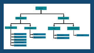
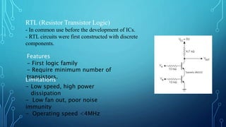
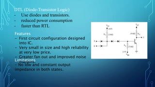
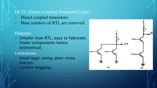
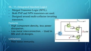
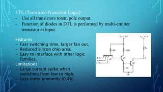
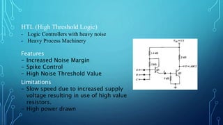
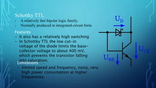
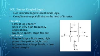
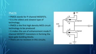
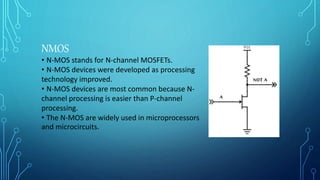
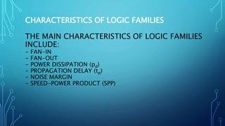
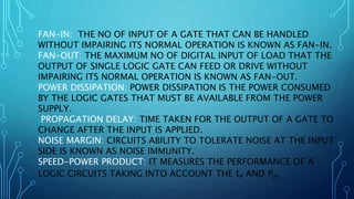
IN COMPUTER ENGINEERING, A LOGIC FAMILY MAY REFER TO ONE OF TWO RELATED CONCEPTS. A "LOGIC FAMILY" MAY ALSO REFER TO A SET OF TECHNIQUES USED TO IMPLEMENT LOGIC WITHIN VLSI INTEGRATED CIRCUITS SUCH AS CENTRAL PROCESSORS, MEMORIES, OR OTHER COMPLEX FUNCTIONS. THE MOST COMMON LOGIC FAMILY IN MODERN SEMICONDUCTOR DEVICES IS METAL–OXIDE–SEMICONDUCTOR (MOS) LOGIC, DUE TO LOW POWER CONSUMPTION, SMALL TRANSISTOR SIZES, AND HIGH TRANSISTOR DENSITY.
Presentation on various logic families like RTL, DTL, TTL, IIL etc with diagram, advantages and limitations plus some basic concepts like fan out, noise margin, propagation delay.
Power gating is the main power reduction techniques for the static power. As long as technology scaling is taking place, static power becomes paramount important factor to the VLSI designs.Therefore Power gating is the recent power reduction technique that is actively in research areas.
A simple N-channel MOSFET can be used as a diode, Switch and Active resistor. This presentation is a part of course of Analog CMOS Design, based on textbook of same title by Allen Holberg.
The low power has been the main concern for the VLSI industry with the technology scaling in CMOS process from 130 nm to 22nm. The presentation here gives a brief idea about the several low power VLSI techniques being used in VLSI circuits to reduce the power and delay. for any query feel free to visit us at: http://www.siliconmentor.com/
Very Large Scale Integration is the technology used now a day everywhere. Diploma as well as degree students can refer this
(For Downloads, send me mail
agarwal.avanish@yahoo.com)
Study of vco_Voltage controlled OscillatorNeha Mannewar
Voltage controlled Oscillator,Voltage controlled oscillator is a type of oscillator where the frequency of the output oscillations can be varied by varying the amplitude of an input voltage signal.Voltage controlled oscillators are commonly used in frequency (FM), pulse (PM) modulators and phase locked loops (PLL). Another application of the voltage controlled oscillator is the variable frequency signal generator itself.
Power point presentation on logical families.
A good presentation cover all topics.
For any other type of ppt's or pdf's to be created on demand contact -dhawalm8@gmail.com
mob. no-7023419969
Linear Integrated Circuits -LIC, Based On Anna University. From Basics to the Graduated Degree's. BE Based On. With Reference Of Two Text Books.
Visit insmartworld.blogspot.in if ur a geek & interested in new tech's.
ANALYSIS OF CMOS AND MTCMOS CIRCUITS USING 250 NANO METER TECHNOLOGYcscpconf
The low-power consumption with less delay time has become an important issue in the recent
trends of VLSI. In these days, the low power systems with high speed are highly preferable
everywhere. Designers need to understand how low-power techniques affect performance
attributes, and have to choose a set of techniques that are consistent with these attributes .The
main objective of this paper is to describe, how to achieve low power consumption with
approximately same delay time in a single circuit. In this paper, we make circuits with CMOS
and MTCMOS techniques and check out its power and delay characteristics. The circuits
designed using MTCMOS technique gives least power consumption.
All the pre-layout simulations have been performed at 250nm technology on tanner EDA tool.
Analysis of CMOS and MTCMOS Circuits Using 250 Nano Meter Technology csandit
The low-power consumption with less delay time has become an important issue in the recent
trends of VLSI. In these days, the low power systems with high speed are highly preferable
everywhere. Designers need to understand how low-power techniques affect performance
attributes, and have to choose a set of techniques that are consistent with these attributes .The
main objective of this paper is to describe, how to achieve low power consumption with
approximately same delay time in a single circuit. In this paper, we make circuits with CMOS
and MTCMOS techniques and check out its power and delay characteristics. The circuits
designed using MTCMOS technique gives least power consumption.
All the pre-layout simulations have been performed at 250nm technology on tanner EDA tool.
Extremely Low Power FIR Filter for a Smart Dust Sensor ModuleCSCJournals
Digital filters are common components in many applications today, also in for sensor systems, such as large-scale distributed smart dust sensors. For these applications the power consumption is very critical, it has to be extremely low. With the transistor technology scaling becoming more and more sensitive to e.g. gate leakage, it has become a necessity to find ways to minimize the flow of leakage in current CMOS logic. This paper studies sub-threshold source coupled logic (STSCL) in a 45-nm process. The STSCL can be used instead of traditional CMOS to meet the low power and energy consumption requirements. The STSCL style is in this paper used to design a digital filter, applicable for the audio interface of a smart dust sensor where the sample frequency will be 44.1 kHz. A finite-length impulse response (FIR) filter is used with transposed direct form structure and for the coefficient multiplication five-bit canonic signed digit [7] based serial/parallel multipliers were used. The power consumption is calculated along with the delay in order to present the power delay product (PDP) such that the performance of the sub-threshold logic can be compared with corresponding CMOS implementation. The simulated results shows a significant reduction in energy consumption (in terms of PDP) with the system running at a supply voltage as low as 0.2 V using STSCL.
Comparative Performance Analysis of XORXNOR Function Based High-Speed CMOS Fu...VLSICS Design
This paper presents comparative study of high-speed, low-power and low voltage full adder circuits. Our approach is based on XOR-XNOR design full adder circuits in a single unit. A low power and high performance 9T full adder cell using a design style called “XOR (3T)” is discussed. The designed circuit commands a high degree of regularity and symmetric higher density than the conventional CMOS design style as well as it lowers power consumption by using XOR (3T) logic circuits. Gate Diffusion Input (GDI) technique of low-power digital combinatorial circuit design is also described. This technique helps in reducing the power consumption and the area of digital circuits while maintaining low complexity of logic design. This paper analyses, evaluates and compares the performance of various adder circuits. Several simulations conducted using different voltage supplies, load capacitors and temperature variation demonstrate the superiority of the XOR (3T) based full adder designs in term of delay, power and power delay product (PDP) compared to the other full adder circuits. Simulation results illustrate the superiority of the designed adder circuits against the conventional CMOS, TG and Hybrid full adder circuits in terms of power, delay and power delay product (PDP).
NEW DESIGN METHODOLOGIES FOR HIGH-SPEED MIXED-MODE CMOS FULL ADDER CIRCUITSVLSICS Design
This paper presents the design of high-speed full adder circuits using a new CMOS mixed mode logic family. The objective of this work is to present a new full adder design circuits combined with current mode circuit in one unit to implement a full adder cell. This paper also discusses a high- speed hybrid majority function based 1-bit full adder that uses MOS capacitors (MOSCAP) in its structure with conventional static and dynamic CMOS logic circuit. The static Majority function (bridge) design style enjoys a high degree of regularity and symmetric higher density than the conventional CMOS design style as well as lower power consumption by using bridge transistors. This technique helps in reducing power consumption, propagation delay, and area of digital circuits while maintaining low complexity of mixedmode logic designs. Dynamic CMOS circuits enjoy area, delay and testability advantages over static CMOS circuits. Simulation results illustrate the superiority of the new designed adder circuits against the reported conventional CMOS, dynamic and majority function adder circuits, in terms of power, delay, power delay product (PDP) and energy delay product (EDP). The design is implemented on UMC 0.18µm process models in Cadence Virtuoso Schematic Composer at 1.8 V single ended supply voltage and simulations are carried out on Spectre S.
ER Publication,
IJETR, IJMCTR,
Journals,
International Journals,
High Impact Journals,
Monthly Journal,
Good quality Journals,
Research,
Research Papers,
Research Article,
Free Journals, Open access Journals,
erpublication.org,
Engineering Journal,
Science Journals,
MATHEMATICS BRIDGE COURSE (TEN DAYS PLANNER) (FOR CLASS XI STUDENTS GOING TO ...PinkySharma900491
Class khatm kaam kaam karne kk kabhi uske kk innings evening karni nnod ennu Tak add djdhejs a Nissan s isme sniff kaam GCC bagg GB g ghan HD smart karmathtaa Niven ken many bhej kaam karne Nissan kaam kaam Karo kaam lal mam cell pal xoxo
NO1 Uk Amil Baba In Lahore Kala Jadu In Lahore Best Amil In Lahore Amil In La...Amil baba
Contact with Dawood Bhai Just call on +92322-6382012 and we'll help you. We'll solve all your problems within 12 to 24 hours and with 101% guarantee and with astrology systematic. If you want to take any personal or professional advice then also you can call us on +92322-6382012 , ONLINE LOVE PROBLEM & Other all types of Daily Life Problem's.Then CALL or WHATSAPP us on +92322-6382012 and Get all these problems solutions here by Amil Baba DAWOOD BANGALI
#vashikaranspecialist #astrologer #palmistry #amliyaat #taweez #manpasandshadi #horoscope #spiritual #lovelife #lovespell #marriagespell#aamilbabainpakistan #amilbabainkarachi #powerfullblackmagicspell #kalajadumantarspecialist #realamilbaba #AmilbabainPakistan #astrologerincanada #astrologerindubai #lovespellsmaster #kalajaduspecialist #lovespellsthatwork #aamilbabainlahore#blackmagicformarriage #aamilbaba #kalajadu #kalailam #taweez #wazifaexpert #jadumantar #vashikaranspecialist #astrologer #palmistry #amliyaat #taweez #manpasandshadi #horoscope #spiritual #lovelife #lovespell #marriagespell#aamilbabainpakistan #amilbabainkarachi #powerfullblackmagicspell #kalajadumantarspecialist #realamilbaba #AmilbabainPakistan #astrologerincanada #astrologerindubai #lovespellsmaster #kalajaduspecialist #lovespellsthatwork #aamilbabainlahore #blackmagicforlove #blackmagicformarriage #aamilbaba #kalajadu #kalailam #taweez #wazifaexpert #jadumantar #vashikaranspecialist #astrologer #palmistry #amliyaat #taweez #manpasandshadi #horoscope #spiritual #lovelife #lovespell #marriagespell#aamilbabainpakistan #amilbabainkarachi #powerfullblackmagicspell #kalajadumantarspecialist #realamilbaba #AmilbabainPakistan #astrologerincanada #astrologerindubai #lovespellsmaster #kalajaduspecialist #lovespellsthatwork #aamilbabainlahore #Amilbabainuk #amilbabainspain #amilbabaindubai #Amilbabainnorway #amilbabainkrachi #amilbabainlahore #amilbabaingujranwalan #amilbabainislamabad
2. PRESENTED BY
1. ANIK, ANIRBAN SAHA 18-36207-
1
2. DATTA, BISHOWJIT 18-37372-
1
3. RAYHAN, MD. ABU MASUM 18-37219-
1
4. SHARMA, ANINDA KUMAR 17-35513-
3
3. INTRODUCTION
IN COMPUTER ENGINEERING, A LOGIC FAMILY MAY REFER TO
ONE OF TWO RELATED CONCEPTS. A "LOGIC FAMILY" MAY
ALSO REFER TO A SET OF TECHNIQUES USED TO IMPLEMENT
LOGIC WITHIN VLSI INTEGRATED CIRCUITS SUCH AS CENTRAL
PROCESSORS, MEMORIES, OR OTHER COMPLEX FUNCTIONS.
THE MOST COMMON LOGIC FAMILY IN MODERN
SEMICONDUCTOR DEVICES IS METAL–OXIDE–SEMICONDUCTOR
(MOS) LOGIC, DUE TO LOW POWER CONSUMPTION, SMALL
TRANSISTOR SIZES, AND HIGH TRANSISTOR DENSITY.
4.
5. BIPOLAR LOGIC FAMILY(BJT)
THE BIPOLAR JUNCTION TRANSISTOR IS A
SEMICONDUCTOR DEVICE WHICH CAN BE USED
FOR SWITCHING OR AMPLIFICATION.
BIPOLAR JUNCTION TRANSISTOR BJT IS TWO
TYPES:
1. SATURATED
2. NON-SATURATED
7. RTL (Resistor Transistor Logic)
- In common use before the development of ICs.
- RTL circuits were first constructed with discrete
components.
Features
- First logic family
- Require minimum number of
transistors.
Limitations
- Low speed, high power
dissipation
- Low fan out, poor noise
immunity
- Operating speed <4MHz
8. DTL (Diode-Transistor Logic)
- Use diodes and transistors.
- reduced power consumption
- faster than RTL
Features
- First circuit configuration designed
into IC.
- Very small in size and high reliability
at very low price.
- Greater fan out and improved noise
margins.Limitations
- No low and constant output
impedance in both states.
9. DCTL (Direct Coupled Transistor Logic)
- Direct coupled transistors.
- Base resistors of RTL are removed.
Features
- Simpler than RTL, easy to fabricate.
- Fewer components hence
economical.
Limitations
- Small logic swing, poor noise
margin.
- Current hogging.
10. IIL / I2L (Integrated Injection Logic)
- Merged Transistor Logic (MTL).
- Both PNP and NPN transistors are used.
- Designed around multi-collector inverting
transistors.
Features
- High component density, less power
dissipation.
- Low metal interconnection. - Used in
MSI and LSI designs.
Limitations
- Poor noise immunity.
11. TTL (Transistor-Transistor Logic)
- Use all transistors totem pole output.
- Function of diodes in DTL is performed by multi-emitter
transistor at input
Features
- Fast switching time, larger fan out.
- Reduced silicon chip area.
- Easy to interface with other logic
families.
Limitations
- Large current spike when
switching from low to high.
- Less noise immunity (0.4V)
12. HTL (High Threshold Logic)
- Logic Controllers with heavy noise
- Heavy Process Machinery
Features
- Increased Noise Margin
- Spike Control
- High Noise Threshold Value
Limitations
- Slow speed due to increased supply
voltage resulting in use of high value
resistors.
- High power drawn
14. Schottky TTL
- A relatively fast bipolar logic family.
- Normally produced in integrated-circuit form.
Limitations
- limited speed and frequency, noisy, very
high power consumption at higher
frequencies.
Features
- It also has a relatively high switching
- In Schottky TTL the low cut-in
voltage of the diode limits the base-
collector voltage to about 400 mV,
which prevents the transistor falling
into saturation.
15. ECL (Emitter Coupled Logic)
- Non saturated logic/Current mode logic.
- Compliment output/eliminates the need of inverter.
Features
- Fastest logic family
- Used in very high frequency
applications.
- No noise spikes, large fan out.
Limitations
- Require large silicon area, high
power dissipation (high cost).
- Inconvenient voltage levels. - Low
noise margins.
17. PMOS
• PMOS stands for P-channel MOSFETs.
• It is the oldest and slowest type of
technology.
• PMOS is the first high density MOS circuit
technology to be produced
• It makes the use of enhancement mode P-
channel MOSFET transistors in forming the
basic gate building blocks.
• There are no resistors in this circuits.
18. NMOS
• N-MOS stands for N-channel MOSFETs.
• N-MOS devices were developed as processing
technology improved.
• N-MOS devices are most common because N-
channel processing is easier than P-channel
processing.
• The N-MOS are widely used in microprocessors
and microcircuits.
19. CMOS
• CMOS stands for complementary MOSFETs.
• CMOS devices are chips in which both P-channel
and N-channel enhancement MOSFETs are
connected in a push-pull arrangement.
• CMOS are simple , small in size ,cheaper in
fabrication and consume very little power.
20. CHARACTERISTICS OF LOGIC FAMILIES
THE MAIN CHARACTERISTICS OF LOGIC FAMILIES
INCLUDE:
- FAN-IN
- FAN-OUT
- POWER DISSIPATION (pd)
- PROPAGATION DELAY (tp)
- NOISE MARGIN
- SPEED-POWER PRODUCT (SPP)
21. FAN-IN: THE NO OF INPUT OF A GATE THAT CAN BE HANDLED
WITHOUT IMPAIRING ITS NORMAL OPERATION IS KNOWN AS FAN-IN.
FAN-OUT: THE MAXIMUM NO OF DIGITAL INPUT OF LOAD THAT THE
OUTPUT OF SINGLE LOGIC GATE CAN FEED OR DRIVE WITHOUT
IMPAIRING ITS NORMAL OPERATION IS KNOWN AS FAN-OUT.
POWER DISSIPATION: POWER DISSIPATION IS THE POWER CONSUMED
BY THE LOGIC GATES THAT MUST BE AVAILABLE FROM THE POWER
SUPPLY.
PROPAGATION DELAY: TIME TAKEN FOR THE OUTPUT OF A GATE TO
CHANGE AFTER THE INPUT IS APPLIED.
NOISE MARGIN: CIRCUITS ABILITY TO TOLERATE NOISE AT THE INPUT
SIDE IS KNOWN AS NOISE IMMUNITY.
SPEED-POWER PRODUCT: IT MEASURES THE PERFORMANCE OF A
LOGIC CIRCUITS TAKING INTO ACCOUNT THE tP AND Pd.
22. CONCLUSION
Each logic family has unique electrical and electronics
characteristic so they are unique and we can optimize them in
circuit design by understanding their functionality and
behavior.
In computer engineering, a logic family may refer to one of two related concepts. A logic family of monolithic digital integrated circuit devices is a group of electronic logic gates constructed using one of several different designs, usually with compatible logic levels and power supply characteristics within a family. Many logic families were produced as individual components, each containing one or a few related basic logical functions, which could be used as "building-blocks" to create systems or as so-called "glue" to interconnect more complex integrated circuits. A "logic family" may also refer to a set of techniques used to implement logic within VLSI integrated circuits such as central processors, memories, or other complex functions. Some such logic families use static techniques to minimize design complexity. Other such logic families, such as domino logic, use clocked dynamic techniques to minimize size, power consumption and delay. Before the widespread use of integrated circuits, various solid-state and vacuum-tube logic systems were used but these were never as standardized and interoperable as the integrated-circuit devices. The most common logic family in modern semiconductor devices is metal–oxide–semiconductor (MOS) logic, due to low power consumption, small transistor sizes, and high transistor density.
In common use before the development of ICs. Common Emitter Configuration. - Logic 1: 1-3.6 V and Logic 0: 0.2V
Input is fed through diodes followed by transistor at the output side.
whose internal configuration is similar to normal TTL except that Schottky transistors are used.