Downloaded 385 times


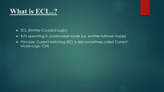
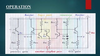
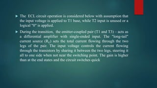


Emitter Coupled Logic (ECL) was invented in 1956 and used transistors operating in an unsaturated mode. ECL uses current switching where the input voltage controls the current flowing through transistor legs. When the input voltage is low or high, one transistor is cut off while the other is active, starving the cut off transistor. ECL provides very fast operation of less than 1 nanosecond but has high power consumption and low noise immunity.


