Downloaded 217 times


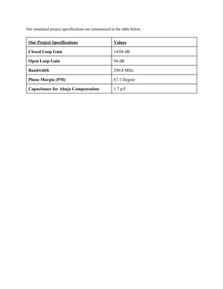
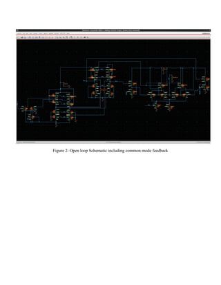
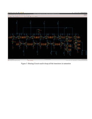
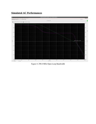
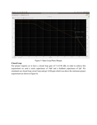
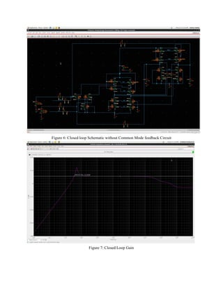
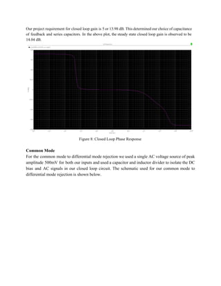
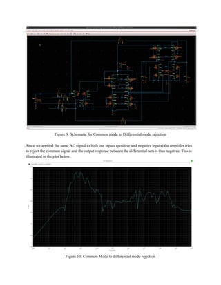
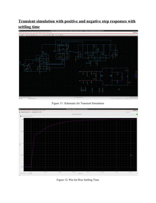
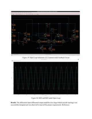

The document details the design of a differential input differential output operational amplifier (op-amp) meeting specific requirements, including a closed loop gain of 5, settling time of 30ns, and supply voltage of 1.8V. The design utilized a two-stage folded cascode architecture and Ahuja compensation for optimal phase margin and bandwidth, resulting in a simulated bandwidth of 290.4MHz and a closed-loop gain of 14.04dB. All project specifications were met, demonstrating the successful implementation of the design approach.