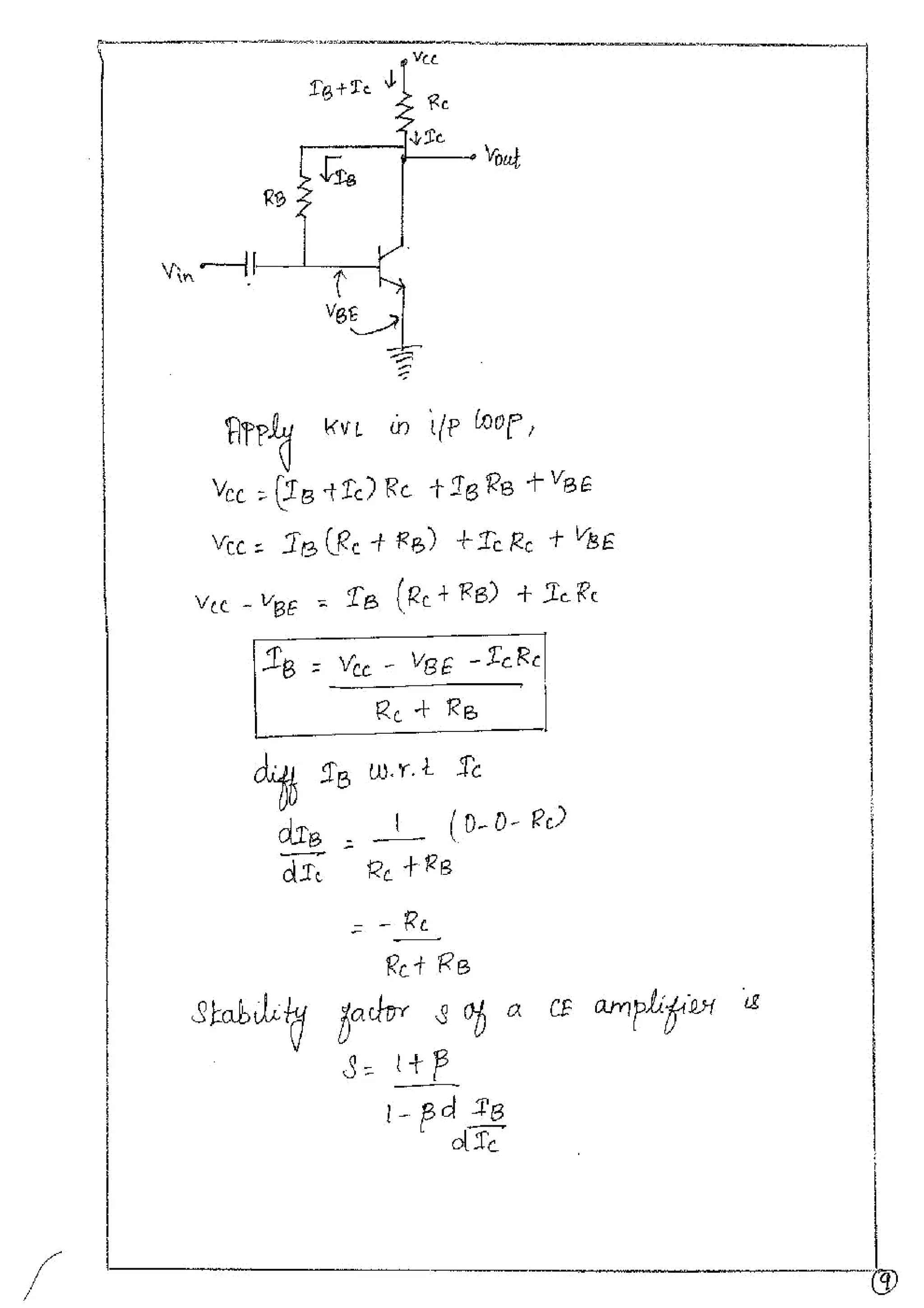
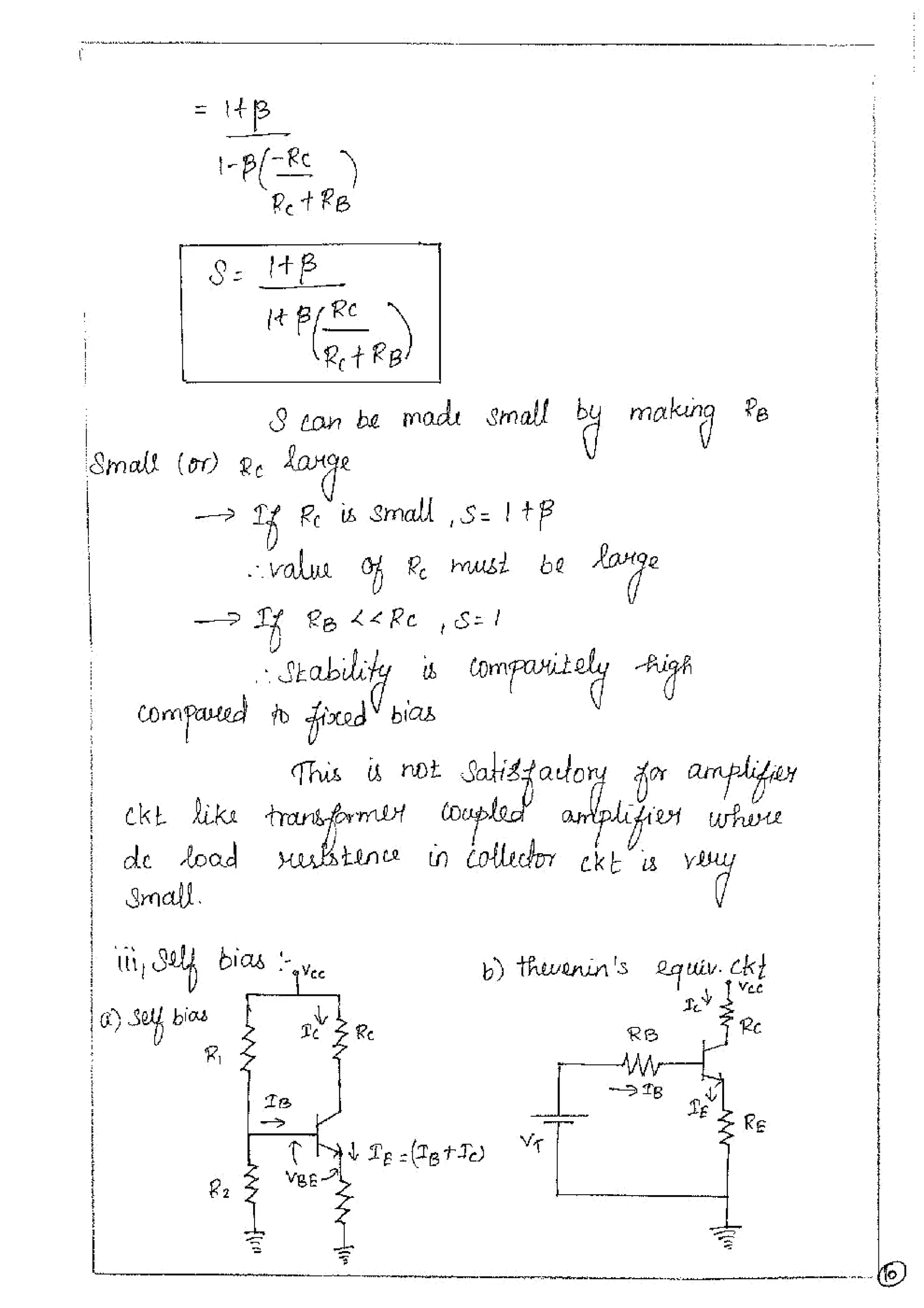
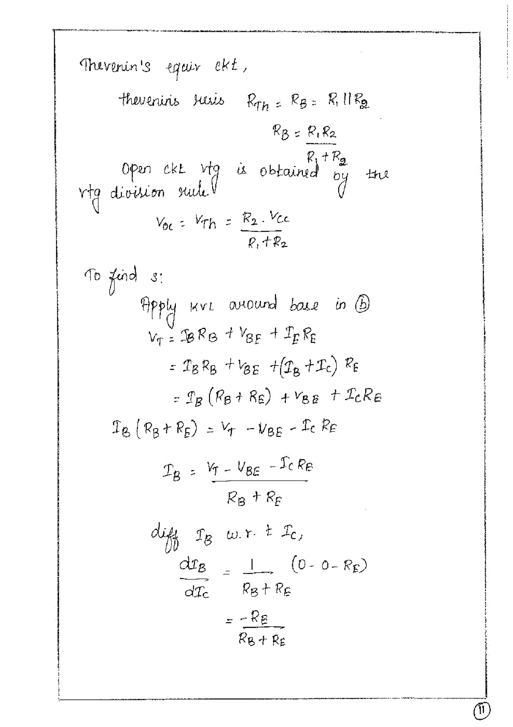
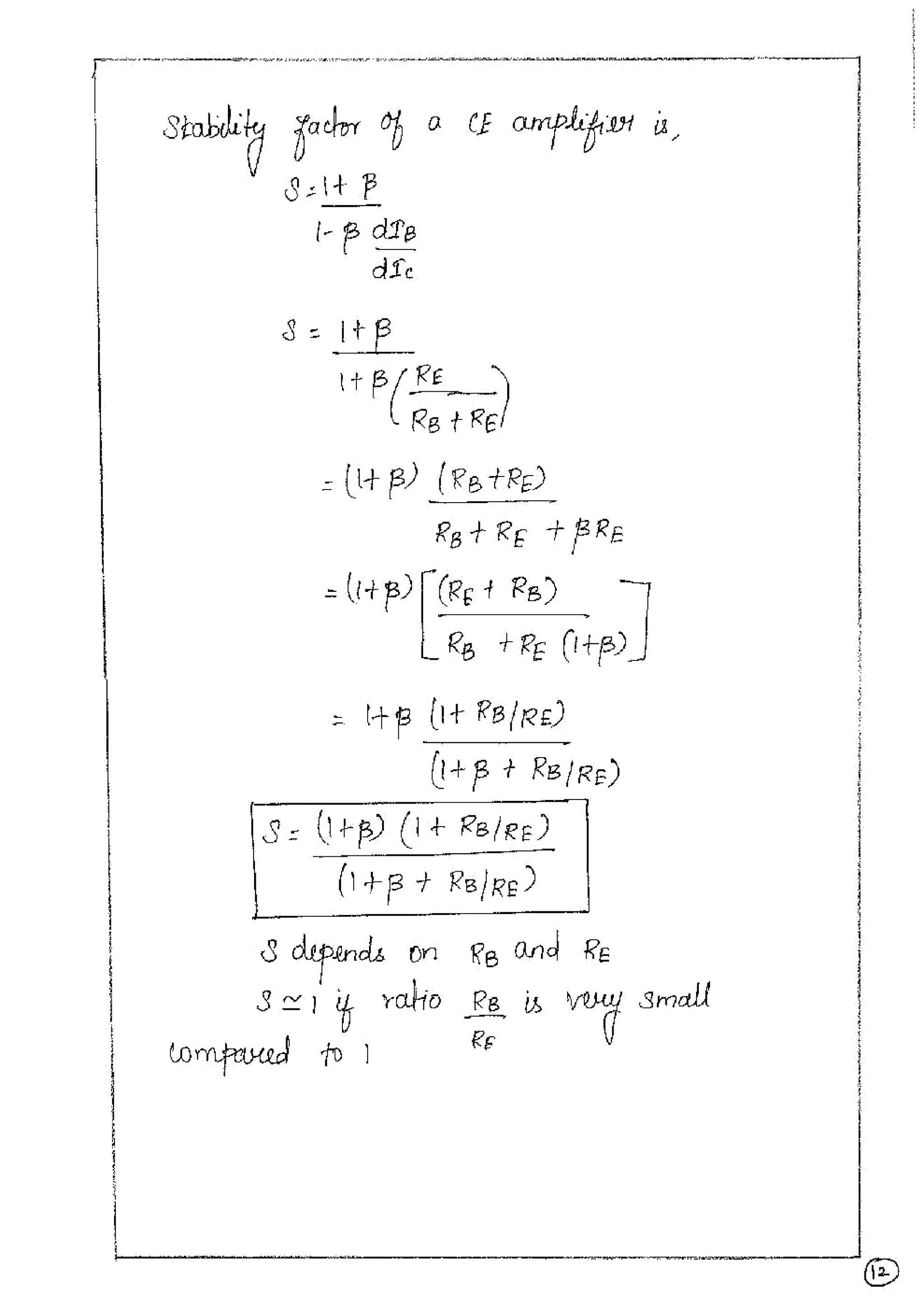
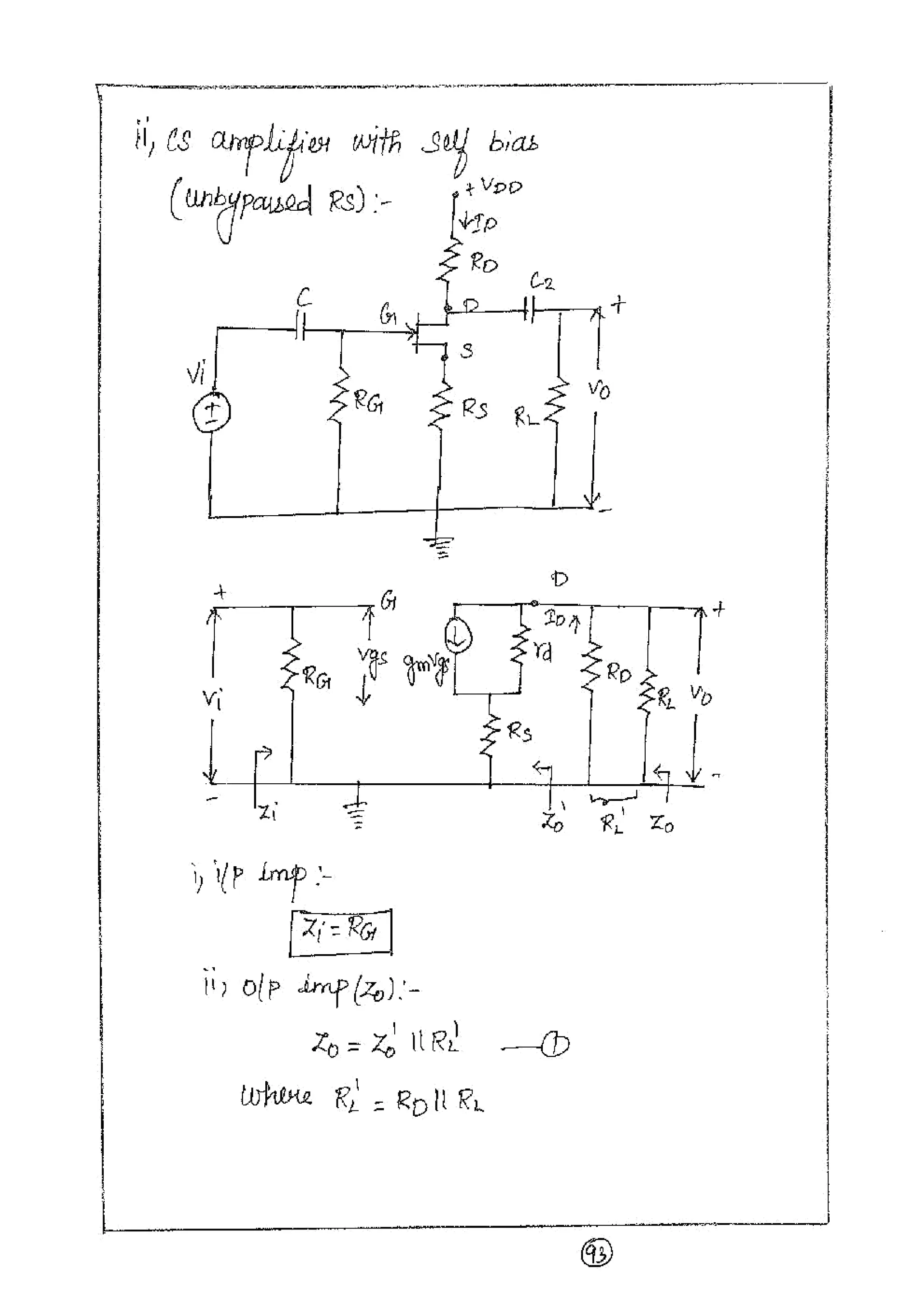
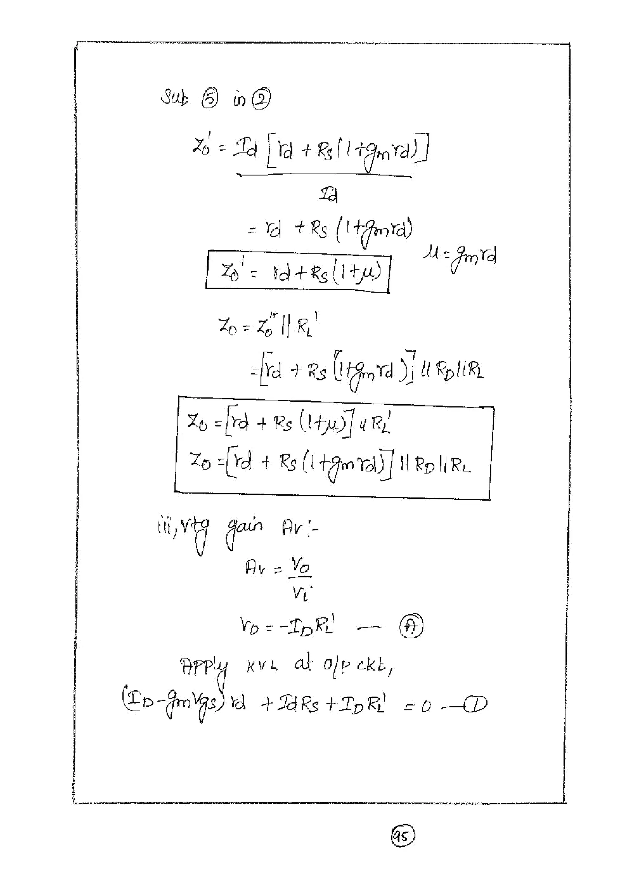
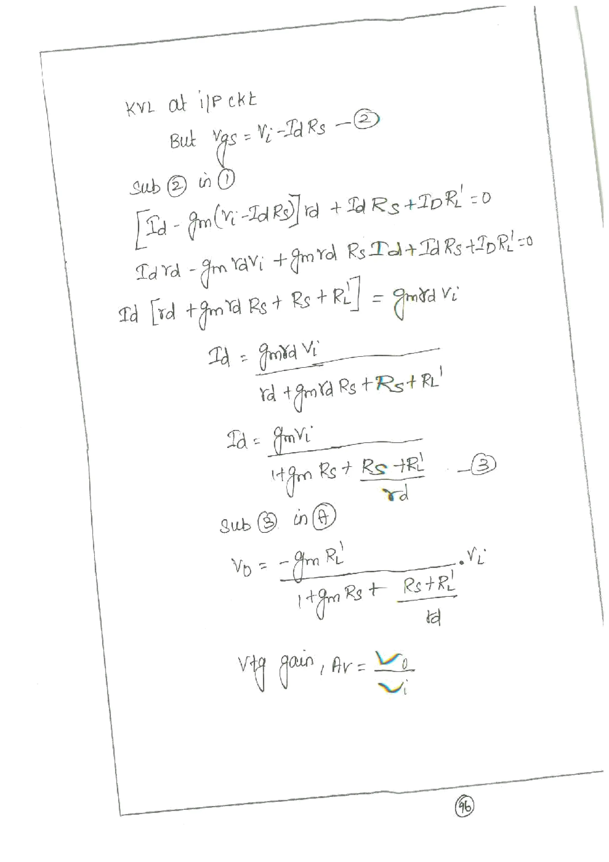
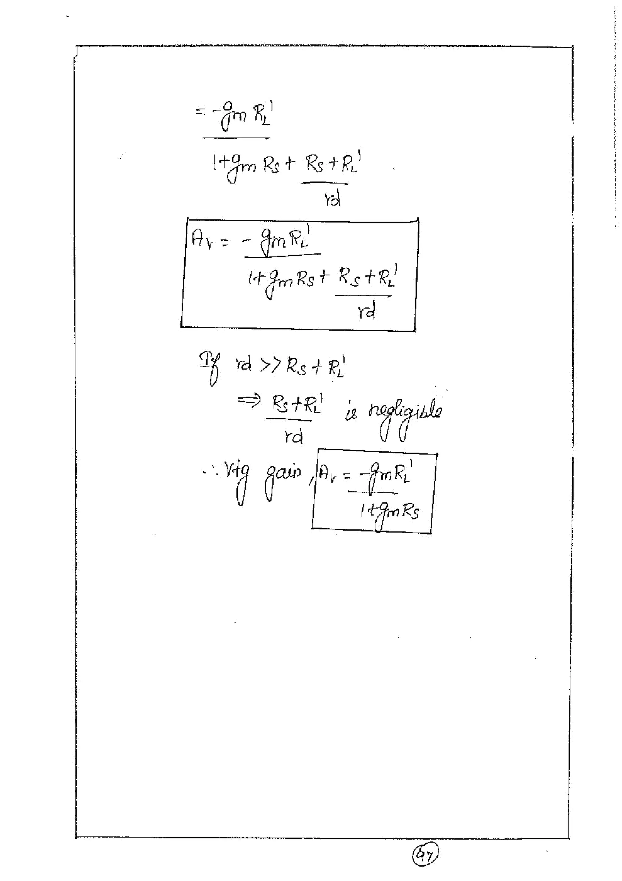
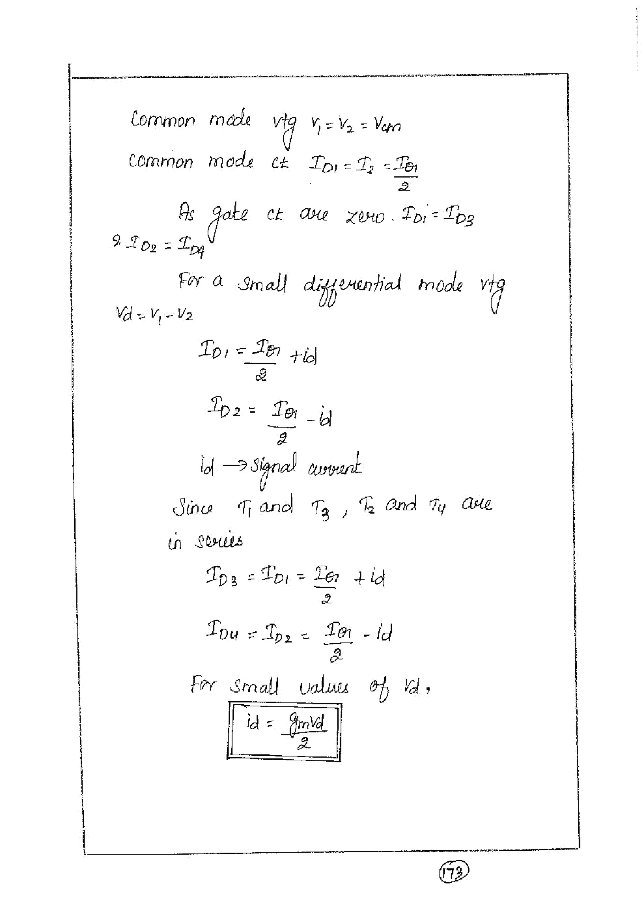
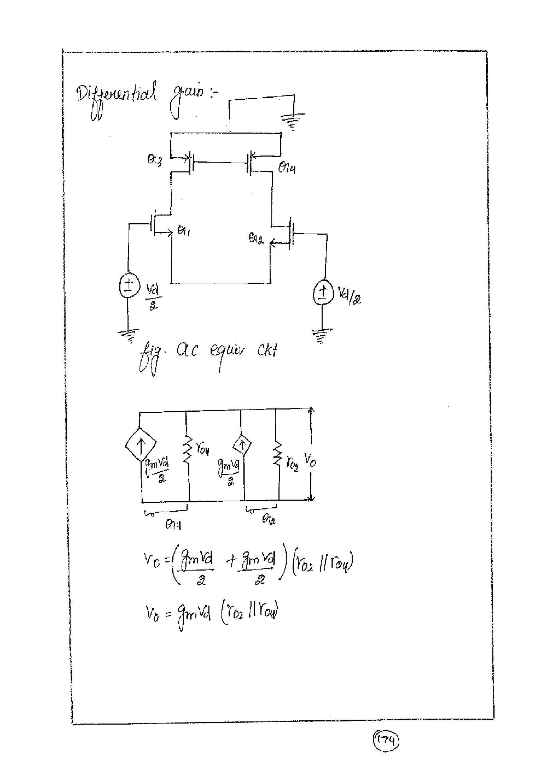
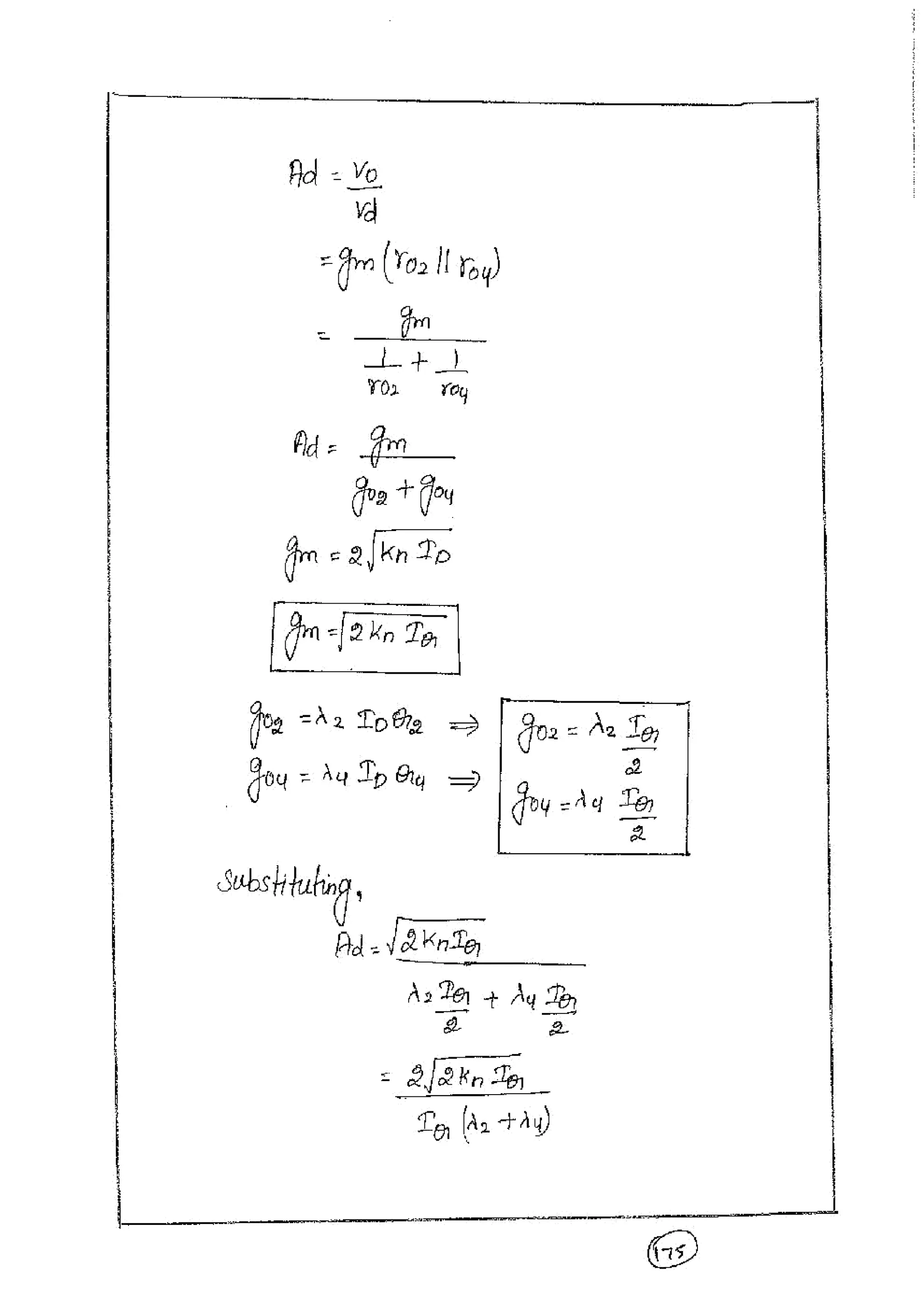
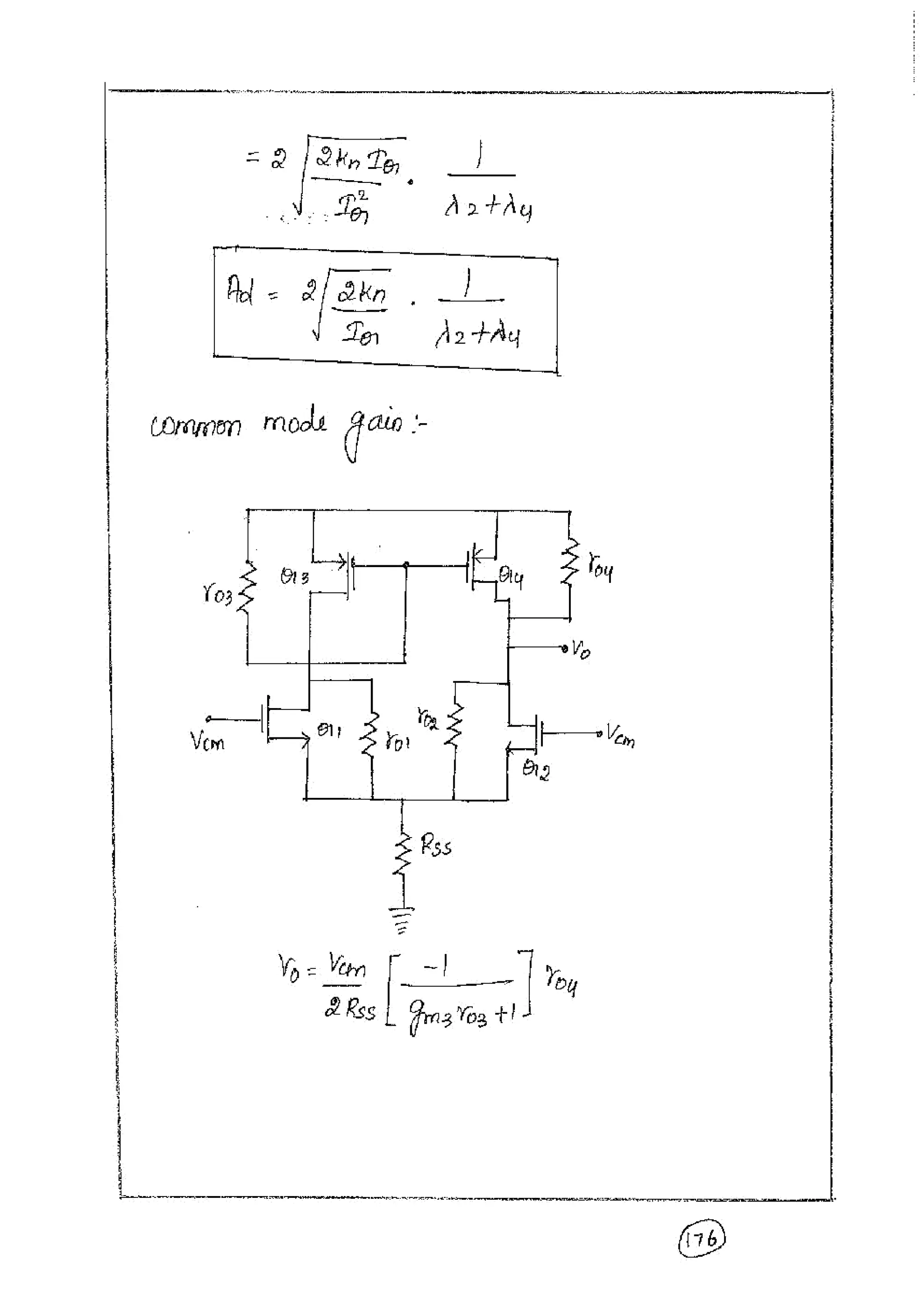
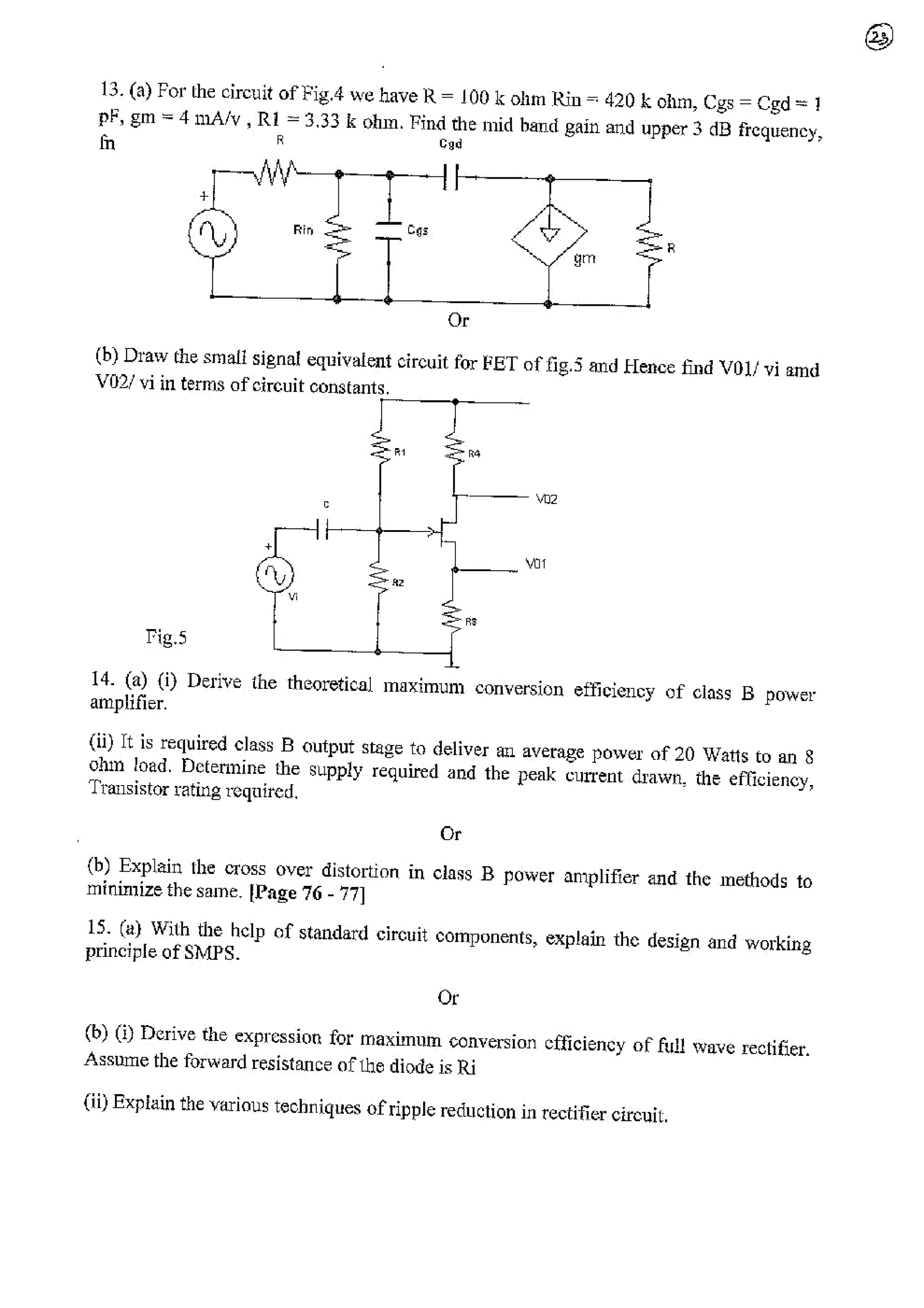
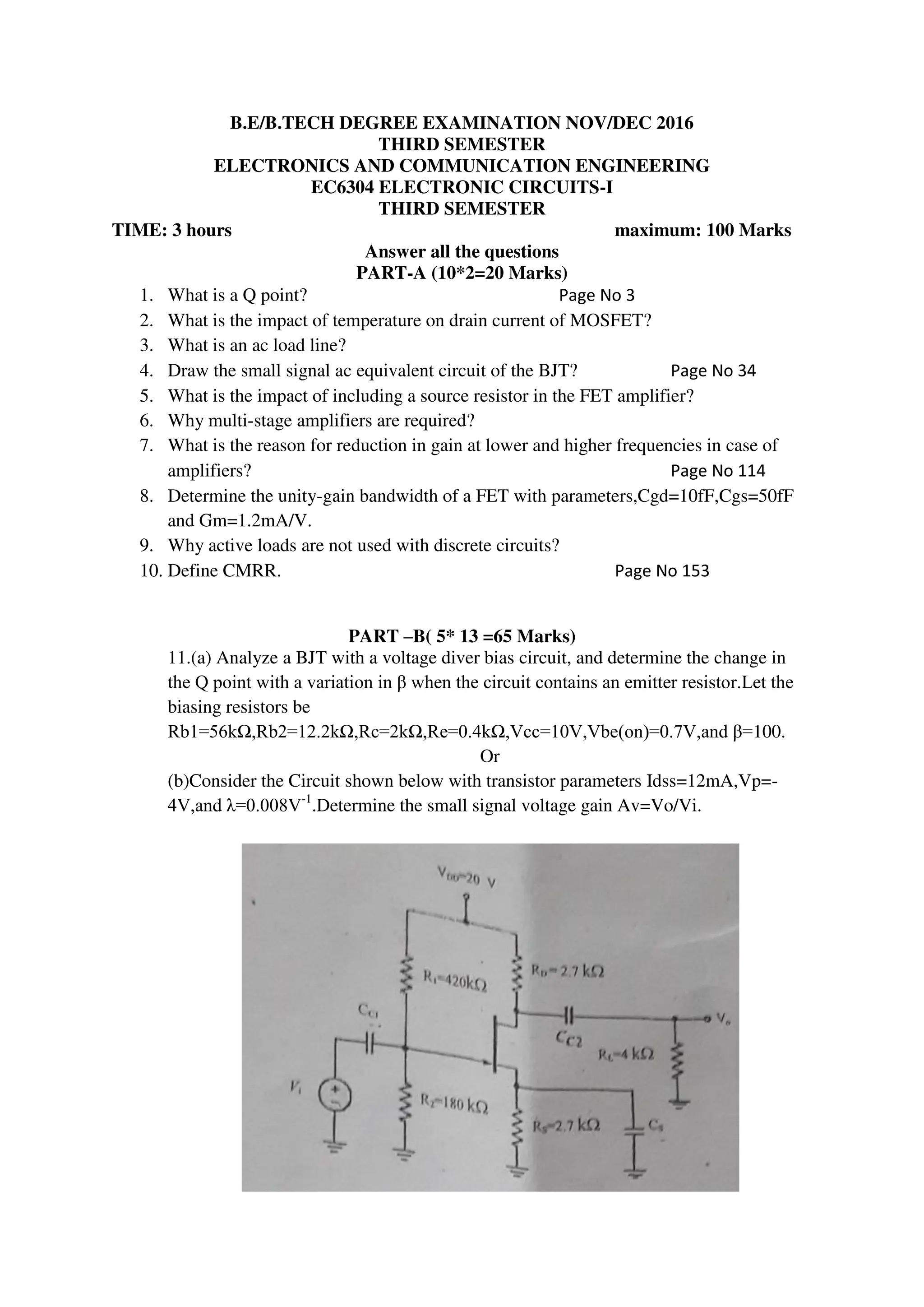
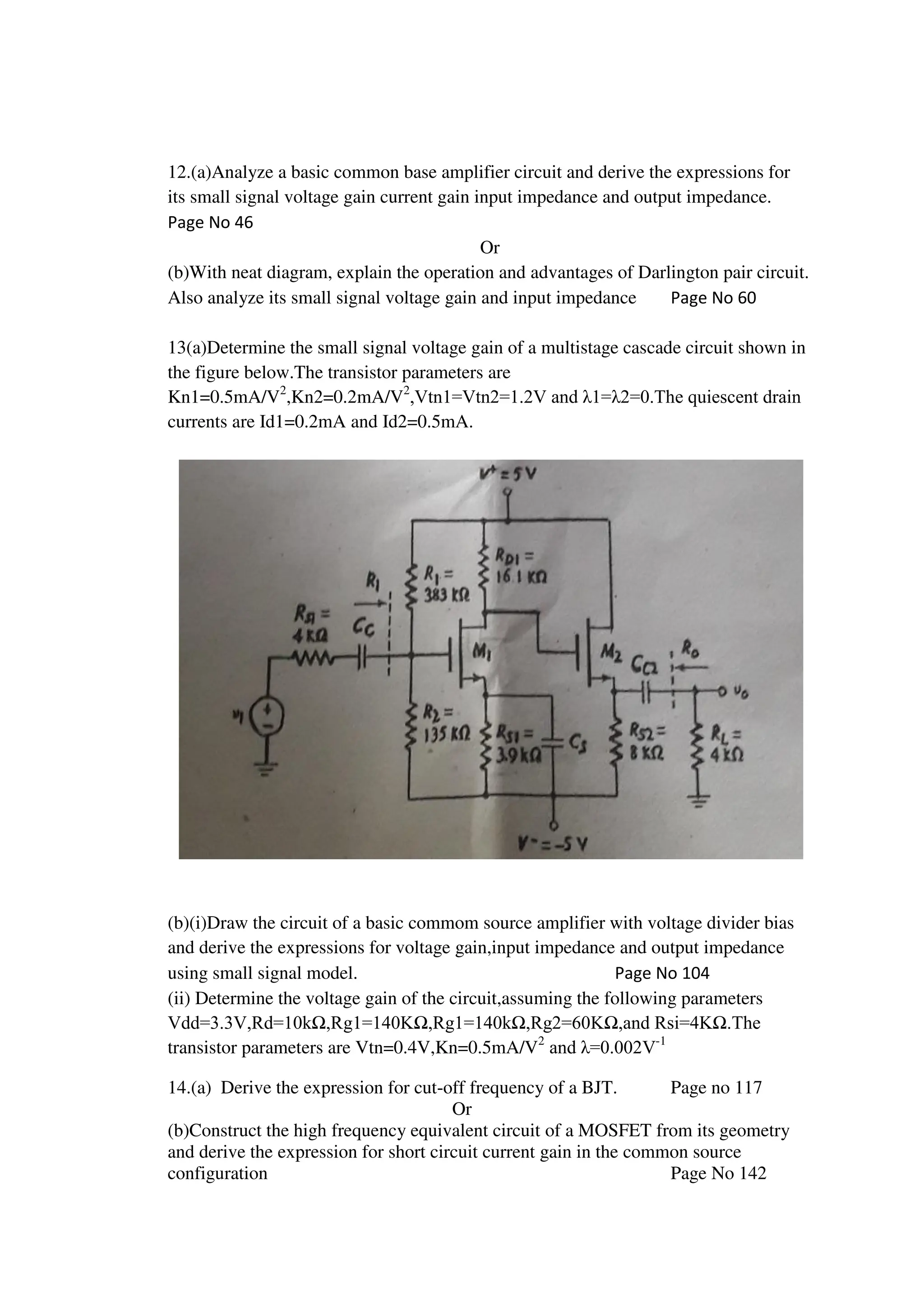
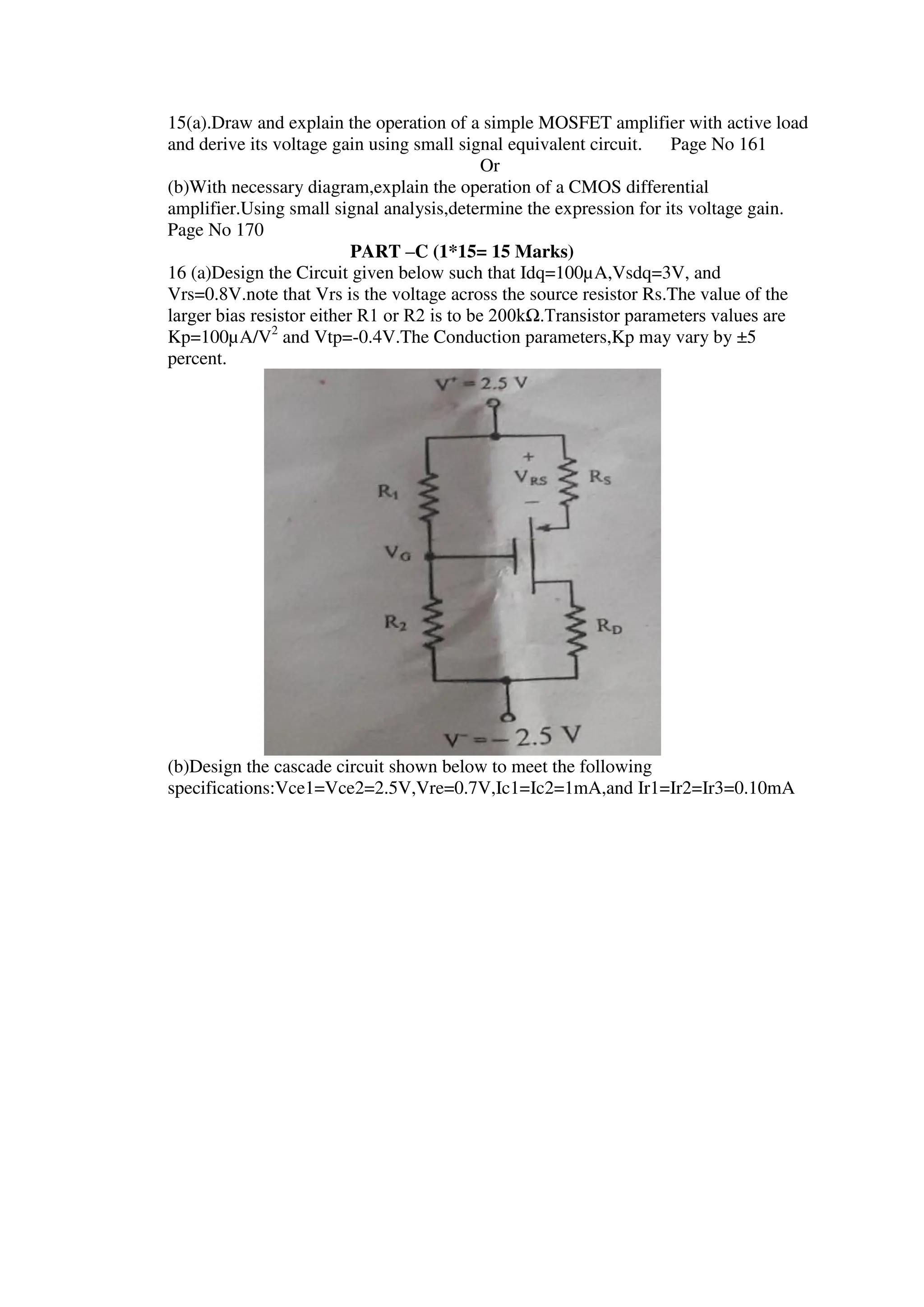
This document contains the course syllabus for Electronic Circuits - I. It includes 5 units that cover various topics related to power supplies, biasing, and amplifiers using BJTs, JFETs, and MOSFETs.
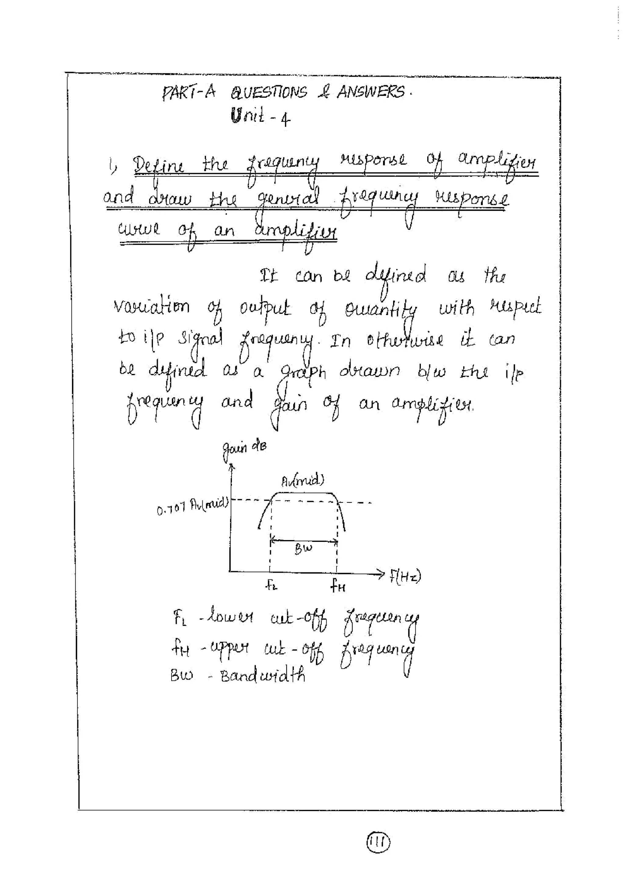
The syllabus outlines the topics that will be covered in each unit, such as rectifiers and power supplies in Unit I, small signal analysis of common emitter, common collector, and common base BJT amplifiers in Unit II, small signal analysis of JFET and MOSFET amplifiers in Unit III, frequency analysis of BJT and MOSFET amplifiers in Unit IV, and IC MOSFET amplifiers such as current sources and differential amplifiers in Unit V