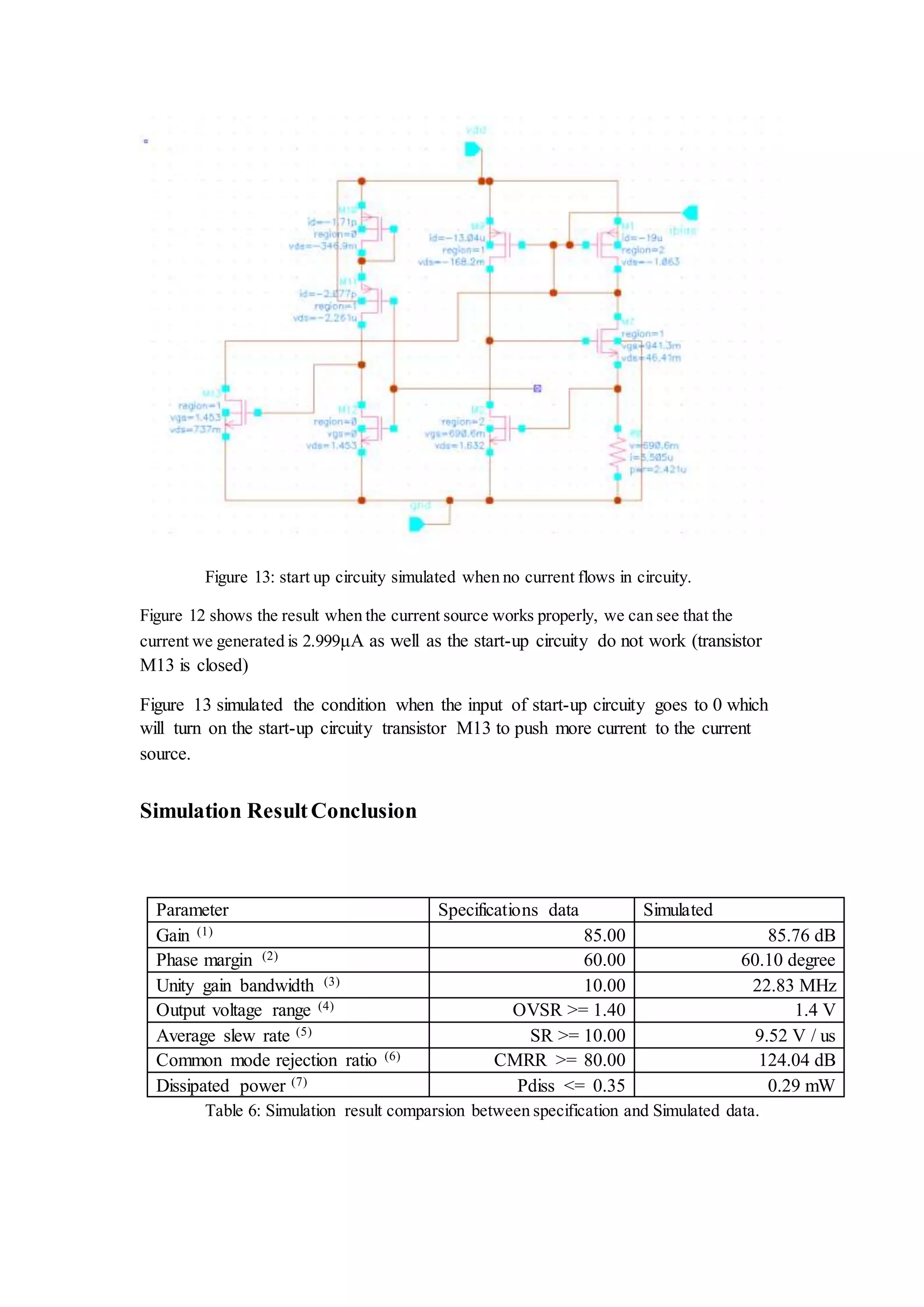
Downloaded 182 times
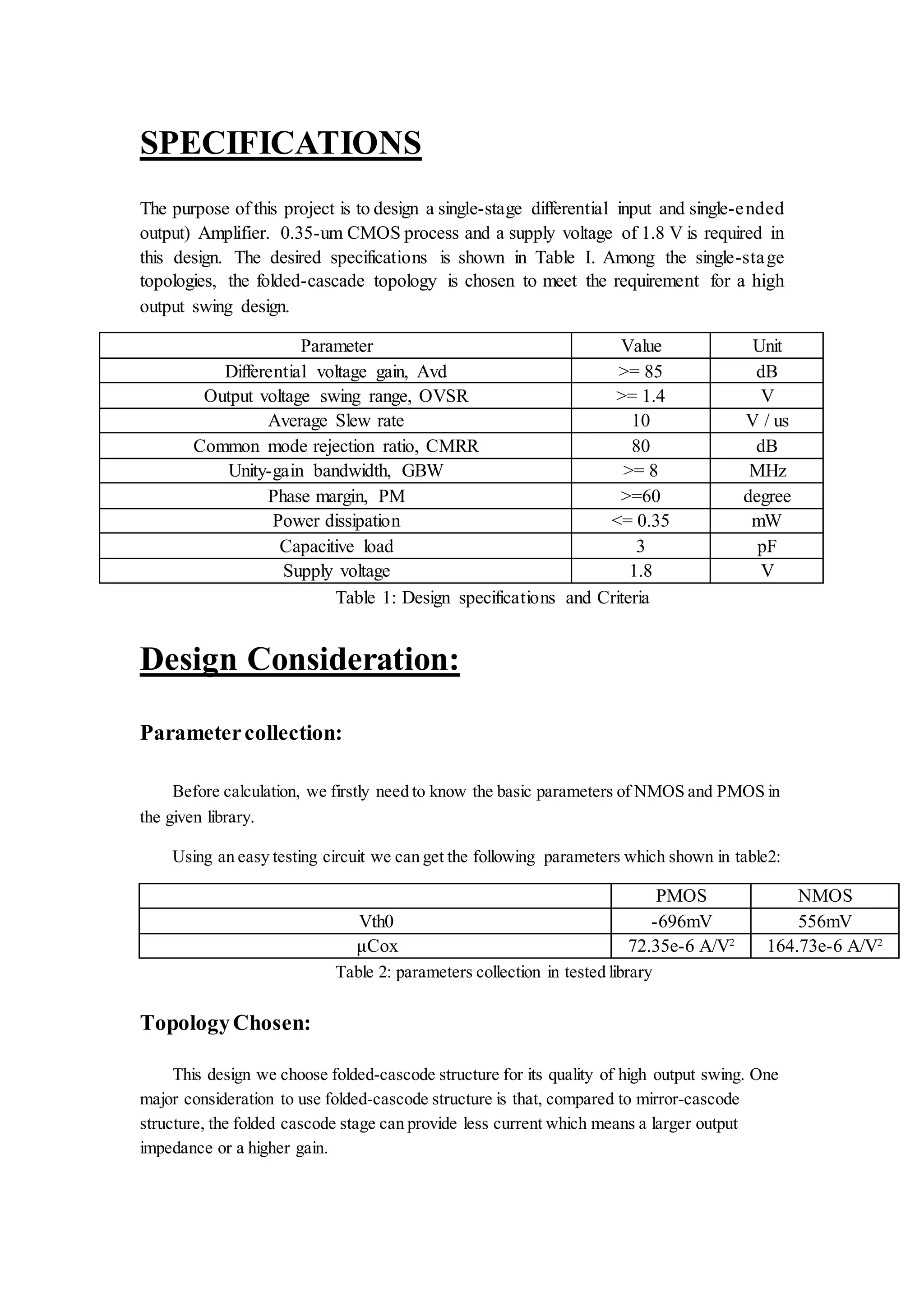
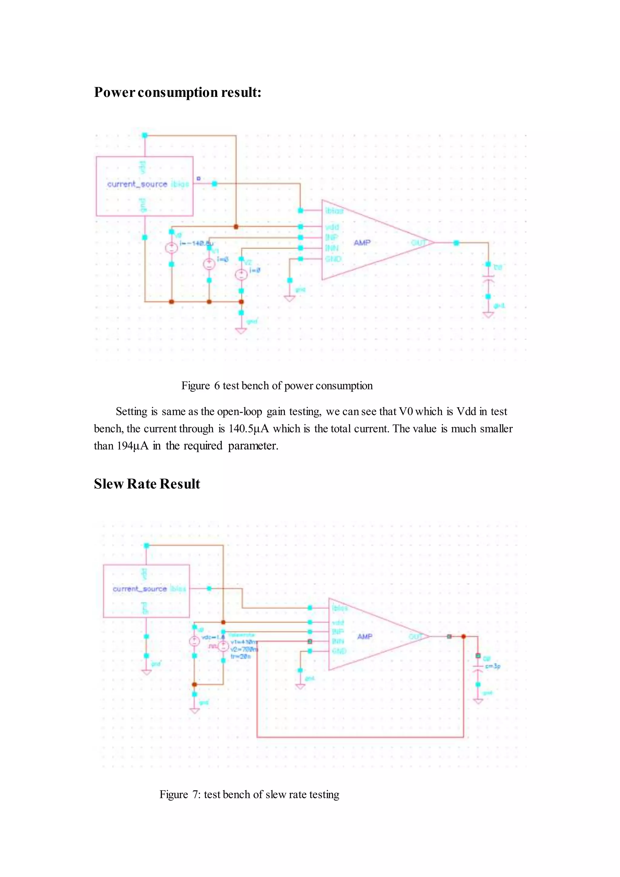
![Powerconsumption consideration:
The power consumption is required to be less than 0.35mW which means the total current
under 1.8V supply voltage is 194μA. The current budget of 194μA mostly should be
distributed to the amplifier stage. Assume the differential pair tail current 𝐼 𝐵𝐼𝐴𝑆 is
31μA, the folded cascode tail current is 35μA. It is reasonable that the total power
consumption can be met.
Slew Rate consideration:
In folded Slew rate tail
L
I
SR
C
>= 10V/μs (as required) where LC is 3pF. We get
𝐼 𝐵𝐼𝐴𝑆 is larger than 30 μA. We assume the 𝐼 𝐵𝐼𝐴𝑆 is 31μA.
Open loop gain consideration:
The open-loop gain is a function of transconductance and the output impedance,
where transconductance is proportional to √ 𝐼 𝐵𝐼𝐴𝑆 /2 and the output impedance is
proportional to
1
𝐼𝐿𝑜𝑎𝑑
. The expression for the open-loop gain is given below with respect
to circuit diagram in Figure 1:
outv RgmA 2,1 ; lowerupperout RRR // ]1[ 1190911 rogmroroRuppper ;
)]//(1[)//( 12029101202 rrgmrrrRlower
From equation, we can find that, for a bigger open loop gain, a small 𝐼𝐿𝑜𝑎𝑑 in folded
cascode part and a big load of 𝐼 𝐵𝐼𝐴𝑆 is needed
W/L ratio calculationfor differential pair:
For the required GBW >= 10MHz, from equation m
L
g
GBW
C
,we get the minimum
transconductance
*m Lg GBW C
= 10MHz * 2*π*3pF = 188.49 μA/V.](https://image.slidesharecdn.com/ee6326finalreport-foldedcascode-151217131914/75/Single-Stage-Differential-Folded-Cascode-Amplifier-3-2048.jpg)
![Since we know the current passing through differential pair i.e. 20uA and also we need
know minimum gm requirement, we can calculate minimum W/L ratio of differential pair
according to equation𝑔 𝑚 = √2𝐼 ∗ μCox(W/L), we get (W/L) 1, 2 min= 3.47
Therefore,the W/L ratio for differential input transistor should be at least 4
Output Voltage Swing considerationand W/L ratio calculationfor
folded cascode part.
The below equation shows the output voltage upper bound and lower bound.
𝑉𝑂𝑈𝑇,𝑚𝑎𝑥 = 𝑉𝐷𝐷 − |2𝑉𝑜𝑣| = 1.8 − 0.2 = 1.6 (1.7)
𝑉𝑂𝑈𝑇,𝑚𝑖𝑛 = 𝑉𝑆𝑆 + 2𝑉𝑜𝑣 = 0 + 0.2 = 0.2 (1.8)
Therefore,to get the desired output swing value, we need to limit the 𝑉𝑜𝑣 within 100
mV.
According to the equation:𝑉𝑜𝑣=√2I/μCox(w/l) ,include before assumption of I =
35μA, we can get the min(W/L)M18,M15 = 96.75;
(W/L)min[M0,M3,M4,M6] =23.67 ; (W/L)min[M5,M19] = 53 (where In = I- Ibias/2
= 19.5uA)
As calculated, we know that to get a high output swing, the minimum W/L for bottom
Nmos is 24, for top Pmos is 97 and 53 separately.](https://image.slidesharecdn.com/ee6326finalreport-foldedcascode-151217131914/75/Single-Stage-Differential-Folded-Cascode-Amplifier-4-2048.jpg)
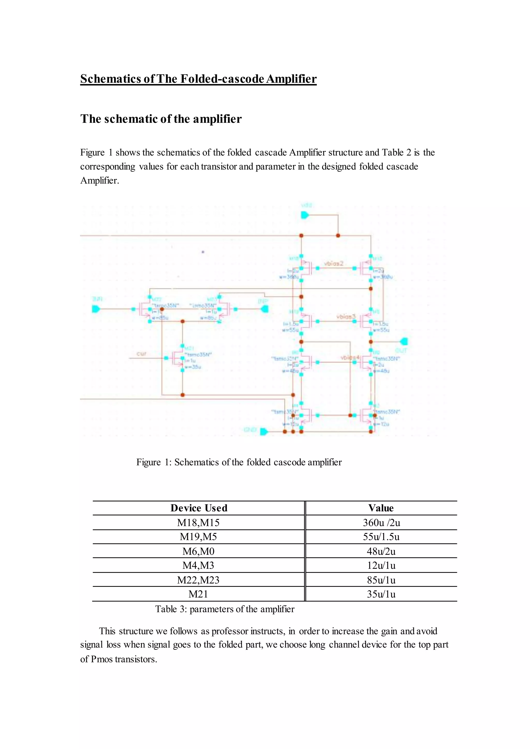
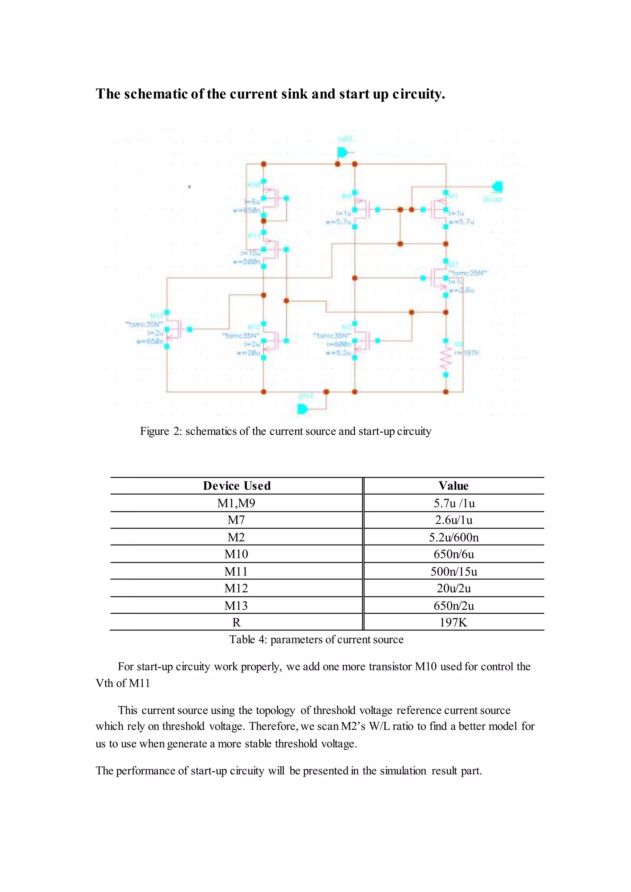
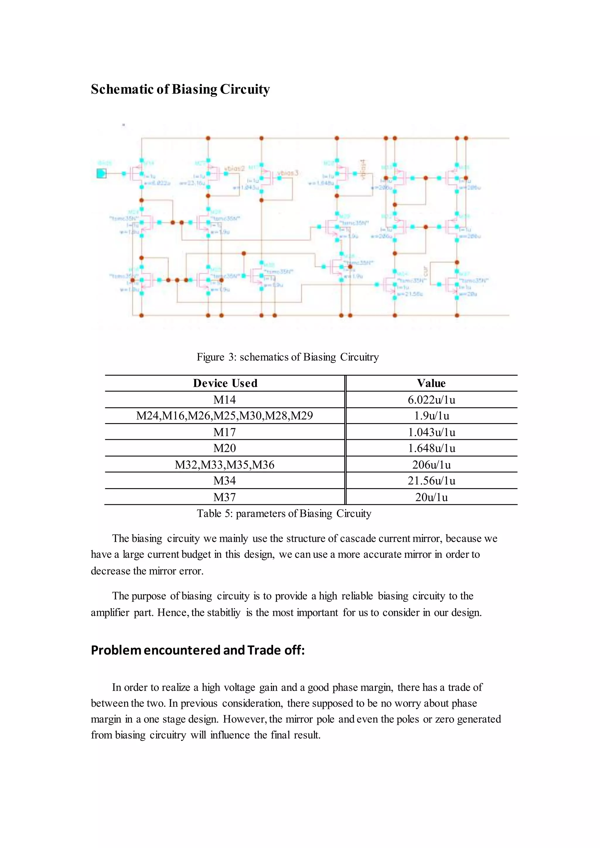
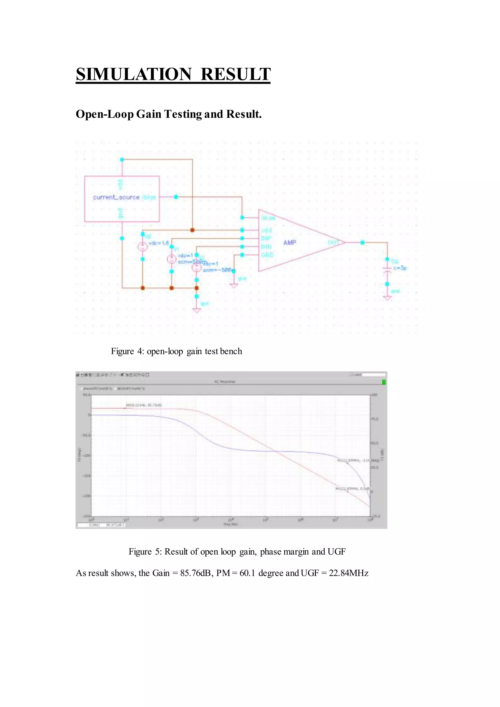
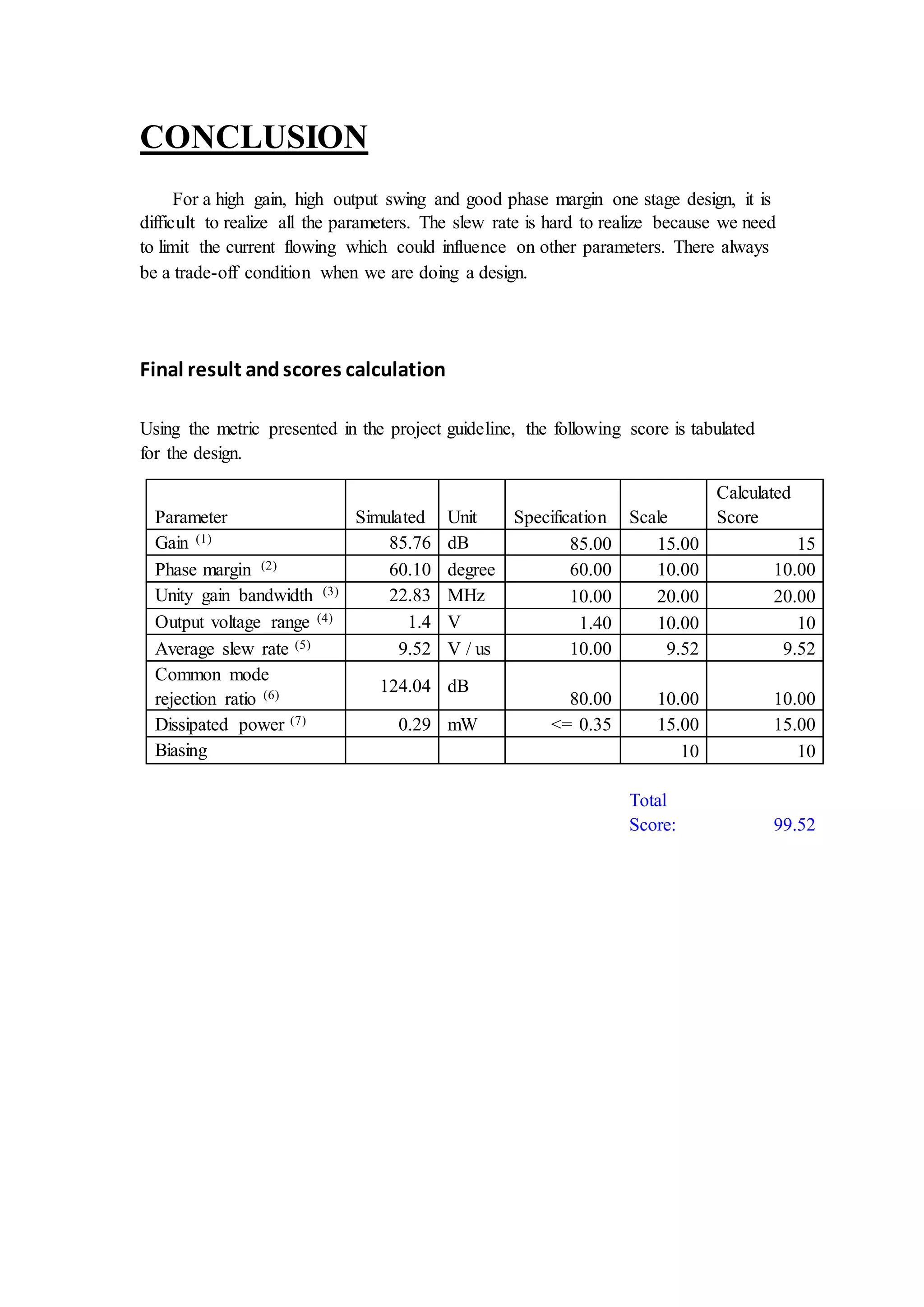

The document presents the final report of a folded cascode amplifier design project. Key aspects of the design include: 1) The amplifier was designed to meet specifications including a gain of 85 dB, output swing of 1.4 V, and slew rate of 10 V/us. 2) A folded cascode topology was chosen to provide high output swing. Transistor sizes were calculated to meet the gain, slew rate, and output swing requirements. 3) Simulation results showed the design met all specifications, with an actual gain of 85.76 dB, phase margin of 60.1 degrees, and slew rate of 9.52 V/us.