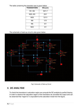
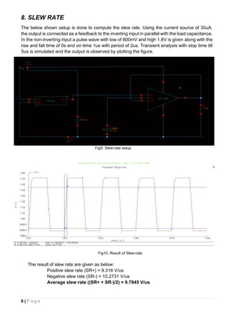
SlideShare a Scribd company logo
1 | P a g e
The University of Texas at Dallas
Department of Electrical Engineering
EECT 6326 ANALOG INTEGRATED CIRCUITS DESIGN
“Differential Current Mirror Two-Stage
Operational Amplifier”
Sriharini Ranganathan (2021255555)
Ilango Jeyasubramanian (202170958)
Ramkishan Gujuluva Nagarajan Dhanlakshmi (2021279911)
2 | P a g e
CONTENTS
1. INTRODUCTION 3
2. DESIGN SPECIFICATIONS 3
3. DESIGN APPROACH 3
4. DESIGN SCHEMATIC 4
5. DC ANALYSIS 5
6. AC ANALYSIS 6
7. OUTPUT VOLTAGE SWING RANGE ANALYSIS 7
8. SLEW RATE 9
9. COMMON MODE REJECTION RATIO 10
10. POWER DISSIPATIONS 11
11. RESULTS 11
12. CONCLUSION 12
13. REFERENCES 12
3 | P a g e
1. INTRODUCTION
The aim of the project is to design a differential input and single ended Two-Stage amplifier.
The amplifier is driven by the 1.8V power source and all the bias currents were generated using
self-biasing current sources and current mirrors instead of ideal current sources. A startup-circuit
has also been used along with the biasing circuit.
To meet the design specifications given below we chose to design a Differential Amplifier with
Current Mirror topology.
2. DESIGN SPECIFICATIONS
• Differential voltage gain: Avd >= 80 dB
• Output voltage swing range: OVSR = Vo(max) – Vo(min) >= 1.45 V
• Average slew rate: SR >= 10V/µs
• Common mode rejection ratio: CMRR >= 80 dB
• Unity-gain bandwidth: GBW >= 8 MHz
• Phase margin: f(GBW) >= 60°
• Power dissipation (VDD): Pdiss ≤ 0.35 mW (1.8V)
• Capacitive load: 3 pF
3. DESIGN APPROACH
1. The first step in the design approach is to calculate the miller-capacitor Cm from the given
load capacitor CL.
2. We know that the transconductance gm1 is much greater than gm6 and assuming the case
we calculated the value of Cm.
3. The value of Slew-rate to be met is given in the Specification chart and from the value of
Cm the tail current I5 is calculated.
4. Similarly Unity Gain Frequency is known and also Cm is known and so the
transcoductance gm1 is calculated. Thus gm6 is also obtained by our assumption.
5. The current flowing through the transistors M1 and M2 is half the current of tail current
I5.
6. With the values of I5 and gm1 the (W/L)1 is calculated and as a current mirror
(W/L)5=(W/L)1.
7. From the Output-swing Voltage Range the VGS under M6 is calculated and also from the
value of gm6 the current I6 is calculated. With the current the (W/L)6 is obtained.
8. The VGS of M6, M4 and M3 are same due to the current mirror configuration and as the
current flowing through them is known (W/L)4=(W/L)3 is calculated.
9. Similarly from the Output-swing the VGS under M7 is also obtained and so the current
flowing through M6 and M7 is same the gm7 is calculated and in turn we get the value of
(W/L)7.
4 | P a g e
10. From the Power dissipation spec the maximum current is known and we set the current
as 16uA that is obtained from the self-biasing current source.
11. As the self-biasing transistor and M7 are current mirrors the (W/L) ratio of the self-
biasing transistor is obtained and so the (W/L)5 is obtained in the similar way.
12. The current mirror circuit is been designed to supply the subsequent bias-voltages in
such a way that all the transistors are in the saturation region (region=2).
13. The start-up circuit was designed as per the lecture notes using the inverter. The desired
current is set by tuning the tail resistor of the start-up mechanism.
14. The desired gain is achieved by the tuning the size of the M5 and also the output
resistance by marginally increased.
15. The major challenge faced by us is to achieve decent slew rate. To achieve a decent
slew rate the output current is controlled which is controlled by the current across M3
and M4.
4. DESIGN SCHEMATIC
Fig1. Schematic of Current Mirror Two-Stage Operational Amplifier
5 | P a g e
The table containing the transistor size is given below:
TRANSISTORS W/L(um)
M1, M2 50/1.7
M25, M3 25/1
M28 121/1
M0 17/1
Mb 6/1
M23 5/1
The schematic of start-up circuit is also given below
Fig2. Schematic of Start-up Circuit
5. DC ANALYSIS
To check the transistors in saturation region we compute the DC analysis by perfect biasing.
In order to observe the saturation region of the transistors we annotate the output and can
be observed that “region=2” is equivalent to the saturation mode from the figure.
6 | P a g e
Fig3. Transistors in the saturation region
As the start-up circuit contains an inverter it is not required that all the transistors should be
in saturation region. In the beginning start-up transistor should always be off and the nmos
of the inverter will be in triode region. Other than these all were in saturation region.
Fig4. Start-up Circuit DC analysis
6. AC ANALYSIS
Before starting the AC analysis the symbol view of the amplifier is created and the
connections VDD, GND, Vin+, Vin- and Vo is created.
7 | P a g e
From the AC analysis the Differential Gain, Phase Margin and Unity Gain Bandwidth are
obtained. To simulate AC analysis the following setup is done with biasing current of 16uA,
VDD at 1.8V, load capacitance 3pF, non-inverting input DC-800mV AC-800mV, and
inverting input DC-800mV AC-800mV. Analysis is done from 0-100MHz and the graph is
plotted.
Fig5. AC Analysis Setup
Fig6. Result: Gain vs Frequency and Phase vs Frequency
It can be seen from the graph that out gain is about 82.74dB. The unity gain bandwidth was
read as 33.54MHz. The phase margin was found to be 60°.
7. OUTPUT VOLTAGE SWING RANGE ANALYSIS
The Output Voltage Swing range is defined as the difference between the maximum and
minimum value that can be achieved by the output voltage. To obtain the analysis following
setup is done.
8 | P a g e
 Apply a DC variable from 0V to 1.8V to the positive input terminal and set 1V DC to
the negative input terminal.
 Apply 16uA to input terminal.
 Apply 1.8V DC between VDD and GND terminal.
 Simulated and the graph obtained is shown below.
Fig7. OVSR Measurement
Fig8. Result of the OVSR simulation
From the above figure OVSR = VO(max) – VO(min) = 1.665 V – 0.09331 V = 1.57169 V
9 | P a g e
8. SLEW RATE
The below shown setup is done to compute the slew rate. Using the current source of 30uA,
the output is connected as a feedback to the inverting input in parallel with the load capacitance.
In the non-inverting input a pulse wave with low of 800mV and high 1.8V is given along with the
rise and fall time of 0s and on-time 1us with period of 2us. Transient analysis with stop time till
5us is simulated and the output is observed by plotting the figure.
Fig9. Slew-rate setup
Fig10. Result of Slew-rate
The result of slew rate are given as below:
Positive slew rate (SR+) = 9.316 V/us
Negative slew rate (SR-) = 10.2731 V/us
Average slew rate ((SR+ + SR-)/2) = 9.7945 V/us
10 | P a g e
9. COMMON MODE REJECTION RATIO
The following setup is done to simulate the CMRR by shorting both the input terminals and are
given a DC and AC voltage 900mV and do AC analysis.
Fig11. CMRR setup
Fig12. Result of Common mode Gain
From the above figure ACM-DM is -5.733 dB
Thus CMRR = 82.74 – (-5.733) = 88.473 dB
11 | P a g e
10. POWER DISSIPATION
From the setup shown below the total current drawn from the source is 123uA. Thus the total
power dissipated is given as Pdiss = 123uA*1.8V = 0.22mW
Fig13. Power dissipation observed through voltage source
11. RESULTS
Parameters Value
Differential Voltage Gain 82.74dB
Phase Margin 60°
Unity Gain Bandwidth 33.54 MHz
Slew Rate 9.7945 V/μs
Output Voltage Swing Range 1.57169V
Common Mode Rejection Ratio 88.473 dB
Power Dissipation 0.22mW
Table1. Result of Current Mirror Operational Amplifier
FINAL SCORE
The final score of the design is calculated using the formula:
As we have used the self-biasing circuit, 10 for biasing
12 | P a g e
Avd(dB) OVSR SR CMRR GBW PM Pdiss
Required ≥80 dB ≥1.45 V ≥10V/us ≥80 dB ≥8 MHz ≥60° ≤0.35 mW
Simulated 82.74dB 1.57169V 9.7945V/us 88.473dB 33.54MHz 60° 0.22mW
Table2. Score for the design
SCORE = 15 + 10 + 9.79 + 10 + 20 + 10 + 15 + 10 = 99.79
12. CONCLUSION
As a whole the Differential Current Mirror Two-Stage Amplifier designed provides higher gain
with higher output voltage swing. In our design only the slew rate is compromised by very
minimal value since it was found to be inversely proportional to the gain.
13. REFERENCES
1. Lee, H, Summer 2015, Analog Integrated Circuit Design, EECT 6326 Class notes,The University of
Texas at Dallas, United States
2. Razavi, B, 2003. Design of Analog CMOS Integrated Circuits. 2nd ed. United States: McGraw Hill
3. Gray, P, 2003. Analysis and Design of Analog Integrated Circuits. 5th ed. United States: Wiley

More Related Content

What's hot

Two stage folded cascode op amp design in Cadence
Two stage folded cascode op amp design in CadenceTwo stage folded cascode op amp design in Cadence
Two stage folded cascode op amp design in Cadence
Karthik Rathinavel
 
Two stage op amp design on cadence
Two stage op amp design on cadenceTwo stage op amp design on cadence
Two stage op amp design on cadence
Haowei Jiang
 
oscillators
 oscillators oscillators
oscillators
vishal gupta
 
Design of optimum self cascode low voltage current mirror
Design of optimum self cascode low voltage current mirrorDesign of optimum self cascode low voltage current mirror
Design of optimum self cascode low voltage current mirror
Ushaswini Chowdary
 
MOSFET....complete PPT
MOSFET....complete PPTMOSFET....complete PPT
MOSFET....complete PPT
Dr. Sanjay M. Gulhane
 
Differential amplifier
Differential amplifierDifferential amplifier
Differential amplifier
sarunkutti
 
Power Amplifier
Power AmplifierPower Amplifier
Power Amplifier
Amit Kumer Podder
 
4. single stage amplifier
4. single stage amplifier4. single stage amplifier
4. single stage amplifier
ShahbazQamar2
 
operational amplifiers
operational amplifiersoperational amplifiers
operational amplifiers
Patel Jay
 
Differential amplifier
Differential amplifierDifferential amplifier
Differential amplifier
srirenga
 
CASCADE AMPLIFIER
CASCADE AMPLIFIERCASCADE AMPLIFIER
CASCADE AMPLIFIER
GLACE VARGHESE T
 
FREQUENCY ENTRAINMENT IN A WIEN BRIDGE OSCILLATOR
FREQUENCY ENTRAINMENT IN A WIEN BRIDGE OSCILLATORFREQUENCY ENTRAINMENT IN A WIEN BRIDGE OSCILLATOR
FREQUENCY ENTRAINMENT IN A WIEN BRIDGE OSCILLATOR
SwgwmsaBoro
 
Power amplifier ppt
Power amplifier pptPower amplifier ppt
Power amplifier ppt
Krishna Ece
 
Amplitude modulation
Amplitude modulationAmplitude modulation
Amplitude modulation
Rumah Belajar
 
Sequential cmos logic circuits
Sequential cmos logic circuitsSequential cmos logic circuits
Sequential cmos logic circuits
Sakshi Bhargava
 
Two-stage CE amplifier
Two-stage CE amplifier Two-stage CE amplifier
Two-stage CE amplifier
mrinal mahato
 
Phase Locked Loop (PLL)
Phase Locked Loop (PLL)Phase Locked Loop (PLL)
Phase Locked Loop (PLL)
Debayon Saha
 
Presentation on Op-amp by Sourabh kumar
Presentation on Op-amp by Sourabh kumarPresentation on Op-amp by Sourabh kumar
Presentation on Op-amp by Sourabh kumar
Sourabh Kumar
 
Summing Amplifier
Summing AmplifierSumming Amplifier
Summing Amplifier
Dr.Raja R
 

What's hot (20)

Two stage folded cascode op amp design in Cadence
Two stage folded cascode op amp design in CadenceTwo stage folded cascode op amp design in Cadence
Two stage folded cascode op amp design in Cadence
 
Two stage op amp design on cadence
Two stage op amp design on cadenceTwo stage op amp design on cadence
Two stage op amp design on cadence
 
oscillators
 oscillators oscillators
oscillators
 
Cadence
CadenceCadence
Cadence
 
Design of optimum self cascode low voltage current mirror
Design of optimum self cascode low voltage current mirrorDesign of optimum self cascode low voltage current mirror
Design of optimum self cascode low voltage current mirror
 
MOSFET....complete PPT
MOSFET....complete PPTMOSFET....complete PPT
MOSFET....complete PPT
 
Differential amplifier
Differential amplifierDifferential amplifier
Differential amplifier
 
Power Amplifier
Power AmplifierPower Amplifier
Power Amplifier
 
4. single stage amplifier
4. single stage amplifier4. single stage amplifier
4. single stage amplifier
 
operational amplifiers
operational amplifiersoperational amplifiers
operational amplifiers
 
Differential amplifier
Differential amplifierDifferential amplifier
Differential amplifier
 
CASCADE AMPLIFIER
CASCADE AMPLIFIERCASCADE AMPLIFIER
CASCADE AMPLIFIER
 
FREQUENCY ENTRAINMENT IN A WIEN BRIDGE OSCILLATOR
FREQUENCY ENTRAINMENT IN A WIEN BRIDGE OSCILLATORFREQUENCY ENTRAINMENT IN A WIEN BRIDGE OSCILLATOR
FREQUENCY ENTRAINMENT IN A WIEN BRIDGE OSCILLATOR
 
Power amplifier ppt
Power amplifier pptPower amplifier ppt
Power amplifier ppt
 
Amplitude modulation
Amplitude modulationAmplitude modulation
Amplitude modulation
 
Sequential cmos logic circuits
Sequential cmos logic circuitsSequential cmos logic circuits
Sequential cmos logic circuits
 
Two-stage CE amplifier
Two-stage CE amplifier Two-stage CE amplifier
Two-stage CE amplifier
 
Phase Locked Loop (PLL)
Phase Locked Loop (PLL)Phase Locked Loop (PLL)
Phase Locked Loop (PLL)
 
Presentation on Op-amp by Sourabh kumar
Presentation on Op-amp by Sourabh kumarPresentation on Op-amp by Sourabh kumar
Presentation on Op-amp by Sourabh kumar
 
Summing Amplifier
Summing AmplifierSumming Amplifier
Summing Amplifier
 

Viewers also liked

Standard cells library design
Standard cells library designStandard cells library design
Standard cells library design
Bharat Biyani
 
ASIC DESIGN OF MINI-STEREO DIGITAL AUDIO PROCESSOR UNDER SMIC 180NM TECHNOLOGY
ASIC DESIGN OF MINI-STEREO DIGITAL AUDIO PROCESSOR UNDER SMIC 180NM TECHNOLOGYASIC DESIGN OF MINI-STEREO DIGITAL AUDIO PROCESSOR UNDER SMIC 180NM TECHNOLOGY
ASIC DESIGN OF MINI-STEREO DIGITAL AUDIO PROCESSOR UNDER SMIC 180NM TECHNOLOGY
Ilango Jeyasubramanian
 
PARASITICS REDUCTION FOR RFIC CMOS LAYOUT AND IIP3 VS Q-BASED DESIGN ANALYSI...
 PARASITICS REDUCTION FOR RFIC CMOS LAYOUT AND IIP3 VS Q-BASED DESIGN ANALYSI... PARASITICS REDUCTION FOR RFIC CMOS LAYOUT AND IIP3 VS Q-BASED DESIGN ANALYSI...
PARASITICS REDUCTION FOR RFIC CMOS LAYOUT AND IIP3 VS Q-BASED DESIGN ANALYSI...
Ilango Jeyasubramanian
 
STANDARD CELL LIBRARY DESIGN
STANDARD CELL LIBRARY DESIGNSTANDARD CELL LIBRARY DESIGN
STANDARD CELL LIBRARY DESIGN
Ilango Jeyasubramanian
 
DESIGNED DYNAMIC SEGMENTED LRU AND MODIFIED MOESI PROTOCOL FOR RING CONNECTED...
DESIGNED DYNAMIC SEGMENTED LRU AND MODIFIED MOESI PROTOCOL FOR RING CONNECTED...DESIGNED DYNAMIC SEGMENTED LRU AND MODIFIED MOESI PROTOCOL FOR RING CONNECTED...
DESIGNED DYNAMIC SEGMENTED LRU AND MODIFIED MOESI PROTOCOL FOR RING CONNECTED...
Ilango Jeyasubramanian
 
PARASITIC-AWARE FULL PHYSICAL CHIP DESIGN OF LNA RFIC AT 2.45GHZ USING IBM 13...
PARASITIC-AWARE FULL PHYSICAL CHIP DESIGN OF LNA RFIC AT 2.45GHZ USING IBM 13...PARASITIC-AWARE FULL PHYSICAL CHIP DESIGN OF LNA RFIC AT 2.45GHZ USING IBM 13...
PARASITIC-AWARE FULL PHYSICAL CHIP DESIGN OF LNA RFIC AT 2.45GHZ USING IBM 13...
Ilango Jeyasubramanian
 

Viewers also liked (6)

Standard cells library design
Standard cells library designStandard cells library design
Standard cells library design
 
ASIC DESIGN OF MINI-STEREO DIGITAL AUDIO PROCESSOR UNDER SMIC 180NM TECHNOLOGY
ASIC DESIGN OF MINI-STEREO DIGITAL AUDIO PROCESSOR UNDER SMIC 180NM TECHNOLOGYASIC DESIGN OF MINI-STEREO DIGITAL AUDIO PROCESSOR UNDER SMIC 180NM TECHNOLOGY
ASIC DESIGN OF MINI-STEREO DIGITAL AUDIO PROCESSOR UNDER SMIC 180NM TECHNOLOGY
 
PARASITICS REDUCTION FOR RFIC CMOS LAYOUT AND IIP3 VS Q-BASED DESIGN ANALYSI...
 PARASITICS REDUCTION FOR RFIC CMOS LAYOUT AND IIP3 VS Q-BASED DESIGN ANALYSI... PARASITICS REDUCTION FOR RFIC CMOS LAYOUT AND IIP3 VS Q-BASED DESIGN ANALYSI...
PARASITICS REDUCTION FOR RFIC CMOS LAYOUT AND IIP3 VS Q-BASED DESIGN ANALYSI...
 
STANDARD CELL LIBRARY DESIGN
STANDARD CELL LIBRARY DESIGNSTANDARD CELL LIBRARY DESIGN
STANDARD CELL LIBRARY DESIGN
 
DESIGNED DYNAMIC SEGMENTED LRU AND MODIFIED MOESI PROTOCOL FOR RING CONNECTED...
DESIGNED DYNAMIC SEGMENTED LRU AND MODIFIED MOESI PROTOCOL FOR RING CONNECTED...DESIGNED DYNAMIC SEGMENTED LRU AND MODIFIED MOESI PROTOCOL FOR RING CONNECTED...
DESIGNED DYNAMIC SEGMENTED LRU AND MODIFIED MOESI PROTOCOL FOR RING CONNECTED...
 
PARASITIC-AWARE FULL PHYSICAL CHIP DESIGN OF LNA RFIC AT 2.45GHZ USING IBM 13...
PARASITIC-AWARE FULL PHYSICAL CHIP DESIGN OF LNA RFIC AT 2.45GHZ USING IBM 13...PARASITIC-AWARE FULL PHYSICAL CHIP DESIGN OF LNA RFIC AT 2.45GHZ USING IBM 13...
PARASITIC-AWARE FULL PHYSICAL CHIP DESIGN OF LNA RFIC AT 2.45GHZ USING IBM 13...
 

Similar to DESIGNED A 350NM TWO STAGE OPERATIONAL AMPLIFIER

A novel voltage reference without the operational amplifier and resistors
A novel voltage reference without the operational amplifier and resistorsA novel voltage reference without the operational amplifier and resistors
A novel voltage reference without the operational amplifier and resistors
IJRES Journal
 
Powerelectronics Chapter7 090331060223 Phpapp02
Powerelectronics Chapter7 090331060223 Phpapp02Powerelectronics Chapter7 090331060223 Phpapp02
Powerelectronics Chapter7 090331060223 Phpapp02
kuppam engg college
 
Power Electronics Chapter 7
Power Electronics  Chapter 7Power Electronics  Chapter 7
Power Electronics Chapter 7
guest8ae54cfb
 
Soft Switched Multi-Output Flyback Converter with Voltage Doubler
Soft Switched Multi-Output Flyback Converter with Voltage DoublerSoft Switched Multi-Output Flyback Converter with Voltage Doubler
Soft Switched Multi-Output Flyback Converter with Voltage Doubler
IJPEDS-IAES
 
Final Project
Final ProjectFinal Project
Final Project
Jeremy Ruppert
 
11 12 sep17 18aug 8416 9975-1-ed (edit)
11 12 sep17 18aug 8416 9975-1-ed (edit)11 12 sep17 18aug 8416 9975-1-ed (edit)
11 12 sep17 18aug 8416 9975-1-ed (edit)
IAESIJEECS
 
A new precision peak detector full wave rectifier
A new precision peak detector full wave rectifierA new precision peak detector full wave rectifier
A new precision peak detector full wave rectifier
Vishal kakade
 
Efitra1006
Efitra1006Efitra1006
Efitra1006
matavulj
 
Project_Kaveh & Mohammad
Project_Kaveh & MohammadProject_Kaveh & Mohammad
Project_Kaveh & Mohammad
Kaveh Dehno
 
506 267-276
506 267-276506 267-276
506 267-276
idescitation
 
Total Harmonic Distortion of Dodecagonal Space Vector Modulation
Total Harmonic Distortion of Dodecagonal Space Vector ModulationTotal Harmonic Distortion of Dodecagonal Space Vector Modulation
Total Harmonic Distortion of Dodecagonal Space Vector Modulation
IJPEDS-IAES
 
Inductorless DC-AC Cascaded H-bridge Multilevel Boost Inverter for Electric/...
Inductorless DC-AC Cascaded H-bridge MultilevelBoost Inverter for Electric/...Inductorless DC-AC Cascaded H-bridge MultilevelBoost Inverter for Electric/...
Inductorless DC-AC Cascaded H-bridge Multilevel Boost Inverter for Electric/...
mkanth
 
Design of Two CMOS Differential Amplifiers
Design of Two CMOS Differential AmplifiersDesign of Two CMOS Differential Amplifiers
Design of Two CMOS Differential Amplifiers
bastrikov
 
A Novel Topology of Multilevel Inverter with Reduced Number of Switches and D...
A Novel Topology of Multilevel Inverter with Reduced Number of Switches and D...A Novel Topology of Multilevel Inverter with Reduced Number of Switches and D...
A Novel Topology of Multilevel Inverter with Reduced Number of Switches and D...
IAES-IJPEDS
 
Level Shifted Discontinuous PWM Algorithms to Minimize Common Mode Voltage fo...
Level Shifted Discontinuous PWM Algorithms to Minimize Common Mode Voltage fo...Level Shifted Discontinuous PWM Algorithms to Minimize Common Mode Voltage fo...
Level Shifted Discontinuous PWM Algorithms to Minimize Common Mode Voltage fo...
International Journal of Power Electronics and Drive Systems
 
6.[36 45]seven level modified cascaded inverter for induction motor drive app...
6.[36 45]seven level modified cascaded inverter for induction motor drive app...6.[36 45]seven level modified cascaded inverter for induction motor drive app...
6.[36 45]seven level modified cascaded inverter for induction motor drive app...
Alexander Decker
 
Asymmetrical Cascaded Multi Level Inverter using Control Freedom Pulse width ...
Asymmetrical Cascaded Multi Level Inverter using Control Freedom Pulse width ...Asymmetrical Cascaded Multi Level Inverter using Control Freedom Pulse width ...
Asymmetrical Cascaded Multi Level Inverter using Control Freedom Pulse width ...
IAES-IJPEDS
 
PWM Switched Voltage Source Inverter with Zero Neutral Point Potential
PWM Switched Voltage Source Inverter with Zero Neutral Point PotentialPWM Switched Voltage Source Inverter with Zero Neutral Point Potential
PWM Switched Voltage Source Inverter with Zero Neutral Point Potential
ijsrd.com
 
Application of SVM Technique for Three Phase Three Leg Ac/Ac Converter Topology
Application of SVM Technique for Three Phase Three Leg Ac/Ac Converter TopologyApplication of SVM Technique for Three Phase Three Leg Ac/Ac Converter Topology
Application of SVM Technique for Three Phase Three Leg Ac/Ac Converter Topology
IOSR Journals
 
Space vector pwm_inverter
Space vector pwm_inverterSpace vector pwm_inverter
Space vector pwm_inverter
ZunAib Ali
 

Similar to DESIGNED A 350NM TWO STAGE OPERATIONAL AMPLIFIER (20)

A novel voltage reference without the operational amplifier and resistors
A novel voltage reference without the operational amplifier and resistorsA novel voltage reference without the operational amplifier and resistors
A novel voltage reference without the operational amplifier and resistors
 
Powerelectronics Chapter7 090331060223 Phpapp02
Powerelectronics Chapter7 090331060223 Phpapp02Powerelectronics Chapter7 090331060223 Phpapp02
Powerelectronics Chapter7 090331060223 Phpapp02
 
Power Electronics Chapter 7
Power Electronics  Chapter 7Power Electronics  Chapter 7
Power Electronics Chapter 7
 
Soft Switched Multi-Output Flyback Converter with Voltage Doubler
Soft Switched Multi-Output Flyback Converter with Voltage DoublerSoft Switched Multi-Output Flyback Converter with Voltage Doubler
Soft Switched Multi-Output Flyback Converter with Voltage Doubler
 
Final Project
Final ProjectFinal Project
Final Project
 
11 12 sep17 18aug 8416 9975-1-ed (edit)
11 12 sep17 18aug 8416 9975-1-ed (edit)11 12 sep17 18aug 8416 9975-1-ed (edit)
11 12 sep17 18aug 8416 9975-1-ed (edit)
 
A new precision peak detector full wave rectifier
A new precision peak detector full wave rectifierA new precision peak detector full wave rectifier
A new precision peak detector full wave rectifier
 
Efitra1006
Efitra1006Efitra1006
Efitra1006
 
Project_Kaveh & Mohammad
Project_Kaveh & MohammadProject_Kaveh & Mohammad
Project_Kaveh & Mohammad
 
506 267-276
506 267-276506 267-276
506 267-276
 
Total Harmonic Distortion of Dodecagonal Space Vector Modulation
Total Harmonic Distortion of Dodecagonal Space Vector ModulationTotal Harmonic Distortion of Dodecagonal Space Vector Modulation
Total Harmonic Distortion of Dodecagonal Space Vector Modulation
 
Inductorless DC-AC Cascaded H-bridge Multilevel Boost Inverter for Electric/...
Inductorless DC-AC Cascaded H-bridge MultilevelBoost Inverter for Electric/...Inductorless DC-AC Cascaded H-bridge MultilevelBoost Inverter for Electric/...
Inductorless DC-AC Cascaded H-bridge Multilevel Boost Inverter for Electric/...
 
Design of Two CMOS Differential Amplifiers
Design of Two CMOS Differential AmplifiersDesign of Two CMOS Differential Amplifiers
Design of Two CMOS Differential Amplifiers
 
A Novel Topology of Multilevel Inverter with Reduced Number of Switches and D...
A Novel Topology of Multilevel Inverter with Reduced Number of Switches and D...A Novel Topology of Multilevel Inverter with Reduced Number of Switches and D...
A Novel Topology of Multilevel Inverter with Reduced Number of Switches and D...
 
Level Shifted Discontinuous PWM Algorithms to Minimize Common Mode Voltage fo...
Level Shifted Discontinuous PWM Algorithms to Minimize Common Mode Voltage fo...Level Shifted Discontinuous PWM Algorithms to Minimize Common Mode Voltage fo...
Level Shifted Discontinuous PWM Algorithms to Minimize Common Mode Voltage fo...
 
6.[36 45]seven level modified cascaded inverter for induction motor drive app...
6.[36 45]seven level modified cascaded inverter for induction motor drive app...6.[36 45]seven level modified cascaded inverter for induction motor drive app...
6.[36 45]seven level modified cascaded inverter for induction motor drive app...
 
Asymmetrical Cascaded Multi Level Inverter using Control Freedom Pulse width ...
Asymmetrical Cascaded Multi Level Inverter using Control Freedom Pulse width ...Asymmetrical Cascaded Multi Level Inverter using Control Freedom Pulse width ...
Asymmetrical Cascaded Multi Level Inverter using Control Freedom Pulse width ...
 
PWM Switched Voltage Source Inverter with Zero Neutral Point Potential
PWM Switched Voltage Source Inverter with Zero Neutral Point PotentialPWM Switched Voltage Source Inverter with Zero Neutral Point Potential
PWM Switched Voltage Source Inverter with Zero Neutral Point Potential
 
Application of SVM Technique for Three Phase Three Leg Ac/Ac Converter Topology
Application of SVM Technique for Three Phase Three Leg Ac/Ac Converter TopologyApplication of SVM Technique for Three Phase Three Leg Ac/Ac Converter Topology
Application of SVM Technique for Three Phase Three Leg Ac/Ac Converter Topology
 
Space vector pwm_inverter
Space vector pwm_inverterSpace vector pwm_inverter
Space vector pwm_inverter
 

Recently uploaded

IEEE Aerospace and Electronic Systems Society as a Graduate Student Member
IEEE Aerospace and Electronic Systems Society as a Graduate Student MemberIEEE Aerospace and Electronic Systems Society as a Graduate Student Member
IEEE Aerospace and Electronic Systems Society as a Graduate Student Member
VICTOR MAESTRE RAMIREZ
 
官方认证美国密歇根州立大学毕业证学位证书原版一模一样
官方认证美国密歇根州立大学毕业证学位证书原版一模一样官方认证美国密歇根州立大学毕业证学位证书原版一模一样
官方认证美国密歇根州立大学毕业证学位证书原版一模一样
171ticu
 
ACEP Magazine edition 4th launched on 05.06.2024
ACEP Magazine edition 4th launched on 05.06.2024ACEP Magazine edition 4th launched on 05.06.2024
ACEP Magazine edition 4th launched on 05.06.2024
Rahul
 
学校原版美国波士顿大学毕业证学历学位证书原版一模一样
学校原版美国波士顿大学毕业证学历学位证书原版一模一样学校原版美国波士顿大学毕业证学历学位证书原版一模一样
学校原版美国波士顿大学毕业证学历学位证书原版一模一样
171ticu
 
Redefining brain tumor segmentation: a cutting-edge convolutional neural netw...
Redefining brain tumor segmentation: a cutting-edge convolutional neural netw...Redefining brain tumor segmentation: a cutting-edge convolutional neural netw...
Redefining brain tumor segmentation: a cutting-edge convolutional neural netw...
IJECEIAES
 
Recycled Concrete Aggregate in Construction Part II
Recycled Concrete Aggregate in Construction Part IIRecycled Concrete Aggregate in Construction Part II
Recycled Concrete Aggregate in Construction Part II
Aditya Rajan Patra
 
Eric Nizeyimana's document 2006 from gicumbi to ttc nyamata handball play
Eric Nizeyimana's document 2006 from gicumbi to ttc nyamata handball playEric Nizeyimana's document 2006 from gicumbi to ttc nyamata handball play
Eric Nizeyimana's document 2006 from gicumbi to ttc nyamata handball play
enizeyimana36
 
A SYSTEMATIC RISK ASSESSMENT APPROACH FOR SECURING THE SMART IRRIGATION SYSTEMS
A SYSTEMATIC RISK ASSESSMENT APPROACH FOR SECURING THE SMART IRRIGATION SYSTEMSA SYSTEMATIC RISK ASSESSMENT APPROACH FOR SECURING THE SMART IRRIGATION SYSTEMS
A SYSTEMATIC RISK ASSESSMENT APPROACH FOR SECURING THE SMART IRRIGATION SYSTEMS
IJNSA Journal
 
22CYT12-Unit-V-E Waste and its Management.ppt
22CYT12-Unit-V-E Waste and its Management.ppt22CYT12-Unit-V-E Waste and its Management.ppt
22CYT12-Unit-V-E Waste and its Management.ppt
KrishnaveniKrishnara1
 
Electric vehicle and photovoltaic advanced roles in enhancing the financial p...
Electric vehicle and photovoltaic advanced roles in enhancing the financial p...Electric vehicle and photovoltaic advanced roles in enhancing the financial p...
Electric vehicle and photovoltaic advanced roles in enhancing the financial p...
IJECEIAES
 
A review on techniques and modelling methodologies used for checking electrom...
A review on techniques and modelling methodologies used for checking electrom...A review on techniques and modelling methodologies used for checking electrom...
A review on techniques and modelling methodologies used for checking electrom...
nooriasukmaningtyas
 
Recycled Concrete Aggregate in Construction Part III
Recycled Concrete Aggregate in Construction Part IIIRecycled Concrete Aggregate in Construction Part III
Recycled Concrete Aggregate in Construction Part III
Aditya Rajan Patra
 
Presentation of IEEE Slovenia CIS (Computational Intelligence Society) Chapte...
Presentation of IEEE Slovenia CIS (Computational Intelligence Society) Chapte...Presentation of IEEE Slovenia CIS (Computational Intelligence Society) Chapte...
Presentation of IEEE Slovenia CIS (Computational Intelligence Society) Chapte...
University of Maribor
 
哪里办理(csu毕业证书)查尔斯特大学毕业证硕士学历原版一模一样
哪里办理(csu毕业证书)查尔斯特大学毕业证硕士学历原版一模一样哪里办理(csu毕业证书)查尔斯特大学毕业证硕士学历原版一模一样
哪里办理(csu毕业证书)查尔斯特大学毕业证硕士学历原版一模一样
insn4465
 
Harnessing WebAssembly for Real-time Stateless Streaming Pipelines
Harnessing WebAssembly for Real-time Stateless Streaming PipelinesHarnessing WebAssembly for Real-time Stateless Streaming Pipelines
Harnessing WebAssembly for Real-time Stateless Streaming Pipelines
Christina Lin
 
Modelagem de um CSTR com reação endotermica.pdf
Modelagem de um CSTR com reação endotermica.pdfModelagem de um CSTR com reação endotermica.pdf
Modelagem de um CSTR com reação endotermica.pdf
camseq
 
Advanced control scheme of doubly fed induction generator for wind turbine us...
Advanced control scheme of doubly fed induction generator for wind turbine us...Advanced control scheme of doubly fed induction generator for wind turbine us...
Advanced control scheme of doubly fed induction generator for wind turbine us...
IJECEIAES
 
Comparative analysis between traditional aquaponics and reconstructed aquapon...
Comparative analysis between traditional aquaponics and reconstructed aquapon...Comparative analysis between traditional aquaponics and reconstructed aquapon...
Comparative analysis between traditional aquaponics and reconstructed aquapon...
bijceesjournal
 
132/33KV substation case study Presentation
132/33KV substation case study Presentation132/33KV substation case study Presentation
132/33KV substation case study Presentation
kandramariana6
 
KuberTENes Birthday Bash Guadalajara - K8sGPT first impressions
KuberTENes Birthday Bash Guadalajara - K8sGPT first impressionsKuberTENes Birthday Bash Guadalajara - K8sGPT first impressions
KuberTENes Birthday Bash Guadalajara - K8sGPT first impressions
Victor Morales
 

Recently uploaded (20)

IEEE Aerospace and Electronic Systems Society as a Graduate Student Member
IEEE Aerospace and Electronic Systems Society as a Graduate Student MemberIEEE Aerospace and Electronic Systems Society as a Graduate Student Member
IEEE Aerospace and Electronic Systems Society as a Graduate Student Member
 
官方认证美国密歇根州立大学毕业证学位证书原版一模一样
官方认证美国密歇根州立大学毕业证学位证书原版一模一样官方认证美国密歇根州立大学毕业证学位证书原版一模一样
官方认证美国密歇根州立大学毕业证学位证书原版一模一样
 
ACEP Magazine edition 4th launched on 05.06.2024
ACEP Magazine edition 4th launched on 05.06.2024ACEP Magazine edition 4th launched on 05.06.2024
ACEP Magazine edition 4th launched on 05.06.2024
 
学校原版美国波士顿大学毕业证学历学位证书原版一模一样
学校原版美国波士顿大学毕业证学历学位证书原版一模一样学校原版美国波士顿大学毕业证学历学位证书原版一模一样
学校原版美国波士顿大学毕业证学历学位证书原版一模一样
 
Redefining brain tumor segmentation: a cutting-edge convolutional neural netw...
Redefining brain tumor segmentation: a cutting-edge convolutional neural netw...Redefining brain tumor segmentation: a cutting-edge convolutional neural netw...
Redefining brain tumor segmentation: a cutting-edge convolutional neural netw...
 
Recycled Concrete Aggregate in Construction Part II
Recycled Concrete Aggregate in Construction Part IIRecycled Concrete Aggregate in Construction Part II
Recycled Concrete Aggregate in Construction Part II
 
Eric Nizeyimana's document 2006 from gicumbi to ttc nyamata handball play
Eric Nizeyimana's document 2006 from gicumbi to ttc nyamata handball playEric Nizeyimana's document 2006 from gicumbi to ttc nyamata handball play
Eric Nizeyimana's document 2006 from gicumbi to ttc nyamata handball play
 
A SYSTEMATIC RISK ASSESSMENT APPROACH FOR SECURING THE SMART IRRIGATION SYSTEMS
A SYSTEMATIC RISK ASSESSMENT APPROACH FOR SECURING THE SMART IRRIGATION SYSTEMSA SYSTEMATIC RISK ASSESSMENT APPROACH FOR SECURING THE SMART IRRIGATION SYSTEMS
A SYSTEMATIC RISK ASSESSMENT APPROACH FOR SECURING THE SMART IRRIGATION SYSTEMS
 
22CYT12-Unit-V-E Waste and its Management.ppt
22CYT12-Unit-V-E Waste and its Management.ppt22CYT12-Unit-V-E Waste and its Management.ppt
22CYT12-Unit-V-E Waste and its Management.ppt
 
Electric vehicle and photovoltaic advanced roles in enhancing the financial p...
Electric vehicle and photovoltaic advanced roles in enhancing the financial p...Electric vehicle and photovoltaic advanced roles in enhancing the financial p...
Electric vehicle and photovoltaic advanced roles in enhancing the financial p...
 
A review on techniques and modelling methodologies used for checking electrom...
A review on techniques and modelling methodologies used for checking electrom...A review on techniques and modelling methodologies used for checking electrom...
A review on techniques and modelling methodologies used for checking electrom...
 
Recycled Concrete Aggregate in Construction Part III
Recycled Concrete Aggregate in Construction Part IIIRecycled Concrete Aggregate in Construction Part III
Recycled Concrete Aggregate in Construction Part III
 
Presentation of IEEE Slovenia CIS (Computational Intelligence Society) Chapte...
Presentation of IEEE Slovenia CIS (Computational Intelligence Society) Chapte...Presentation of IEEE Slovenia CIS (Computational Intelligence Society) Chapte...
Presentation of IEEE Slovenia CIS (Computational Intelligence Society) Chapte...
 
哪里办理(csu毕业证书)查尔斯特大学毕业证硕士学历原版一模一样
哪里办理(csu毕业证书)查尔斯特大学毕业证硕士学历原版一模一样哪里办理(csu毕业证书)查尔斯特大学毕业证硕士学历原版一模一样
哪里办理(csu毕业证书)查尔斯特大学毕业证硕士学历原版一模一样
 
Harnessing WebAssembly for Real-time Stateless Streaming Pipelines
Harnessing WebAssembly for Real-time Stateless Streaming PipelinesHarnessing WebAssembly for Real-time Stateless Streaming Pipelines
Harnessing WebAssembly for Real-time Stateless Streaming Pipelines
 
Modelagem de um CSTR com reação endotermica.pdf
Modelagem de um CSTR com reação endotermica.pdfModelagem de um CSTR com reação endotermica.pdf
Modelagem de um CSTR com reação endotermica.pdf
 
Advanced control scheme of doubly fed induction generator for wind turbine us...
Advanced control scheme of doubly fed induction generator for wind turbine us...Advanced control scheme of doubly fed induction generator for wind turbine us...
Advanced control scheme of doubly fed induction generator for wind turbine us...
 
Comparative analysis between traditional aquaponics and reconstructed aquapon...
Comparative analysis between traditional aquaponics and reconstructed aquapon...Comparative analysis between traditional aquaponics and reconstructed aquapon...
Comparative analysis between traditional aquaponics and reconstructed aquapon...
 
132/33KV substation case study Presentation
132/33KV substation case study Presentation132/33KV substation case study Presentation
132/33KV substation case study Presentation
 
KuberTENes Birthday Bash Guadalajara - K8sGPT first impressions
KuberTENes Birthday Bash Guadalajara - K8sGPT first impressionsKuberTENes Birthday Bash Guadalajara - K8sGPT first impressions
KuberTENes Birthday Bash Guadalajara - K8sGPT first impressions
 

DESIGNED A 350NM TWO STAGE OPERATIONAL AMPLIFIER

  • 1. 1 | P a g e The University of Texas at Dallas Department of Electrical Engineering EECT 6326 ANALOG INTEGRATED CIRCUITS DESIGN “Differential Current Mirror Two-Stage Operational Amplifier” Sriharini Ranganathan (2021255555) Ilango Jeyasubramanian (202170958) Ramkishan Gujuluva Nagarajan Dhanlakshmi (2021279911)
  • 2. 2 | P a g e CONTENTS 1. INTRODUCTION 3 2. DESIGN SPECIFICATIONS 3 3. DESIGN APPROACH 3 4. DESIGN SCHEMATIC 4 5. DC ANALYSIS 5 6. AC ANALYSIS 6 7. OUTPUT VOLTAGE SWING RANGE ANALYSIS 7 8. SLEW RATE 9 9. COMMON MODE REJECTION RATIO 10 10. POWER DISSIPATIONS 11 11. RESULTS 11 12. CONCLUSION 12 13. REFERENCES 12
  • 3. 3 | P a g e 1. INTRODUCTION The aim of the project is to design a differential input and single ended Two-Stage amplifier. The amplifier is driven by the 1.8V power source and all the bias currents were generated using self-biasing current sources and current mirrors instead of ideal current sources. A startup-circuit has also been used along with the biasing circuit. To meet the design specifications given below we chose to design a Differential Amplifier with Current Mirror topology. 2. DESIGN SPECIFICATIONS • Differential voltage gain: Avd >= 80 dB • Output voltage swing range: OVSR = Vo(max) – Vo(min) >= 1.45 V • Average slew rate: SR >= 10V/µs • Common mode rejection ratio: CMRR >= 80 dB • Unity-gain bandwidth: GBW >= 8 MHz • Phase margin: f(GBW) >= 60° • Power dissipation (VDD): Pdiss ≤ 0.35 mW (1.8V) • Capacitive load: 3 pF 3. DESIGN APPROACH 1. The first step in the design approach is to calculate the miller-capacitor Cm from the given load capacitor CL. 2. We know that the transconductance gm1 is much greater than gm6 and assuming the case we calculated the value of Cm. 3. The value of Slew-rate to be met is given in the Specification chart and from the value of Cm the tail current I5 is calculated. 4. Similarly Unity Gain Frequency is known and also Cm is known and so the transcoductance gm1 is calculated. Thus gm6 is also obtained by our assumption. 5. The current flowing through the transistors M1 and M2 is half the current of tail current I5. 6. With the values of I5 and gm1 the (W/L)1 is calculated and as a current mirror (W/L)5=(W/L)1. 7. From the Output-swing Voltage Range the VGS under M6 is calculated and also from the value of gm6 the current I6 is calculated. With the current the (W/L)6 is obtained. 8. The VGS of M6, M4 and M3 are same due to the current mirror configuration and as the current flowing through them is known (W/L)4=(W/L)3 is calculated. 9. Similarly from the Output-swing the VGS under M7 is also obtained and so the current flowing through M6 and M7 is same the gm7 is calculated and in turn we get the value of (W/L)7.
  • 4. 4 | P a g e 10. From the Power dissipation spec the maximum current is known and we set the current as 16uA that is obtained from the self-biasing current source. 11. As the self-biasing transistor and M7 are current mirrors the (W/L) ratio of the self- biasing transistor is obtained and so the (W/L)5 is obtained in the similar way. 12. The current mirror circuit is been designed to supply the subsequent bias-voltages in such a way that all the transistors are in the saturation region (region=2). 13. The start-up circuit was designed as per the lecture notes using the inverter. The desired current is set by tuning the tail resistor of the start-up mechanism. 14. The desired gain is achieved by the tuning the size of the M5 and also the output resistance by marginally increased. 15. The major challenge faced by us is to achieve decent slew rate. To achieve a decent slew rate the output current is controlled which is controlled by the current across M3 and M4. 4. DESIGN SCHEMATIC Fig1. Schematic of Current Mirror Two-Stage Operational Amplifier
  • 5. 5 | P a g e The table containing the transistor size is given below: TRANSISTORS W/L(um) M1, M2 50/1.7 M25, M3 25/1 M28 121/1 M0 17/1 Mb 6/1 M23 5/1 The schematic of start-up circuit is also given below Fig2. Schematic of Start-up Circuit 5. DC ANALYSIS To check the transistors in saturation region we compute the DC analysis by perfect biasing. In order to observe the saturation region of the transistors we annotate the output and can be observed that “region=2” is equivalent to the saturation mode from the figure.
  • 6. 6 | P a g e Fig3. Transistors in the saturation region As the start-up circuit contains an inverter it is not required that all the transistors should be in saturation region. In the beginning start-up transistor should always be off and the nmos of the inverter will be in triode region. Other than these all were in saturation region. Fig4. Start-up Circuit DC analysis 6. AC ANALYSIS Before starting the AC analysis the symbol view of the amplifier is created and the connections VDD, GND, Vin+, Vin- and Vo is created.
  • 7. 7 | P a g e From the AC analysis the Differential Gain, Phase Margin and Unity Gain Bandwidth are obtained. To simulate AC analysis the following setup is done with biasing current of 16uA, VDD at 1.8V, load capacitance 3pF, non-inverting input DC-800mV AC-800mV, and inverting input DC-800mV AC-800mV. Analysis is done from 0-100MHz and the graph is plotted. Fig5. AC Analysis Setup Fig6. Result: Gain vs Frequency and Phase vs Frequency It can be seen from the graph that out gain is about 82.74dB. The unity gain bandwidth was read as 33.54MHz. The phase margin was found to be 60°. 7. OUTPUT VOLTAGE SWING RANGE ANALYSIS The Output Voltage Swing range is defined as the difference between the maximum and minimum value that can be achieved by the output voltage. To obtain the analysis following setup is done.
  • 8. 8 | P a g e  Apply a DC variable from 0V to 1.8V to the positive input terminal and set 1V DC to the negative input terminal.  Apply 16uA to input terminal.  Apply 1.8V DC between VDD and GND terminal.  Simulated and the graph obtained is shown below. Fig7. OVSR Measurement Fig8. Result of the OVSR simulation From the above figure OVSR = VO(max) – VO(min) = 1.665 V – 0.09331 V = 1.57169 V
  • 9. 9 | P a g e 8. SLEW RATE The below shown setup is done to compute the slew rate. Using the current source of 30uA, the output is connected as a feedback to the inverting input in parallel with the load capacitance. In the non-inverting input a pulse wave with low of 800mV and high 1.8V is given along with the rise and fall time of 0s and on-time 1us with period of 2us. Transient analysis with stop time till 5us is simulated and the output is observed by plotting the figure. Fig9. Slew-rate setup Fig10. Result of Slew-rate The result of slew rate are given as below: Positive slew rate (SR+) = 9.316 V/us Negative slew rate (SR-) = 10.2731 V/us Average slew rate ((SR+ + SR-)/2) = 9.7945 V/us
  • 10. 10 | P a g e 9. COMMON MODE REJECTION RATIO The following setup is done to simulate the CMRR by shorting both the input terminals and are given a DC and AC voltage 900mV and do AC analysis. Fig11. CMRR setup Fig12. Result of Common mode Gain From the above figure ACM-DM is -5.733 dB Thus CMRR = 82.74 – (-5.733) = 88.473 dB
  • 11. 11 | P a g e 10. POWER DISSIPATION From the setup shown below the total current drawn from the source is 123uA. Thus the total power dissipated is given as Pdiss = 123uA*1.8V = 0.22mW Fig13. Power dissipation observed through voltage source 11. RESULTS Parameters Value Differential Voltage Gain 82.74dB Phase Margin 60° Unity Gain Bandwidth 33.54 MHz Slew Rate 9.7945 V/μs Output Voltage Swing Range 1.57169V Common Mode Rejection Ratio 88.473 dB Power Dissipation 0.22mW Table1. Result of Current Mirror Operational Amplifier FINAL SCORE The final score of the design is calculated using the formula: As we have used the self-biasing circuit, 10 for biasing
  • 12. 12 | P a g e Avd(dB) OVSR SR CMRR GBW PM Pdiss Required ≥80 dB ≥1.45 V ≥10V/us ≥80 dB ≥8 MHz ≥60° ≤0.35 mW Simulated 82.74dB 1.57169V 9.7945V/us 88.473dB 33.54MHz 60° 0.22mW Table2. Score for the design SCORE = 15 + 10 + 9.79 + 10 + 20 + 10 + 15 + 10 = 99.79 12. CONCLUSION As a whole the Differential Current Mirror Two-Stage Amplifier designed provides higher gain with higher output voltage swing. In our design only the slew rate is compromised by very minimal value since it was found to be inversely proportional to the gain. 13. REFERENCES 1. Lee, H, Summer 2015, Analog Integrated Circuit Design, EECT 6326 Class notes,The University of Texas at Dallas, United States 2. Razavi, B, 2003. Design of Analog CMOS Integrated Circuits. 2nd ed. United States: McGraw Hill 3. Gray, P, 2003. Analysis and Design of Analog Integrated Circuits. 5th ed. United States: Wiley