Download to read offline

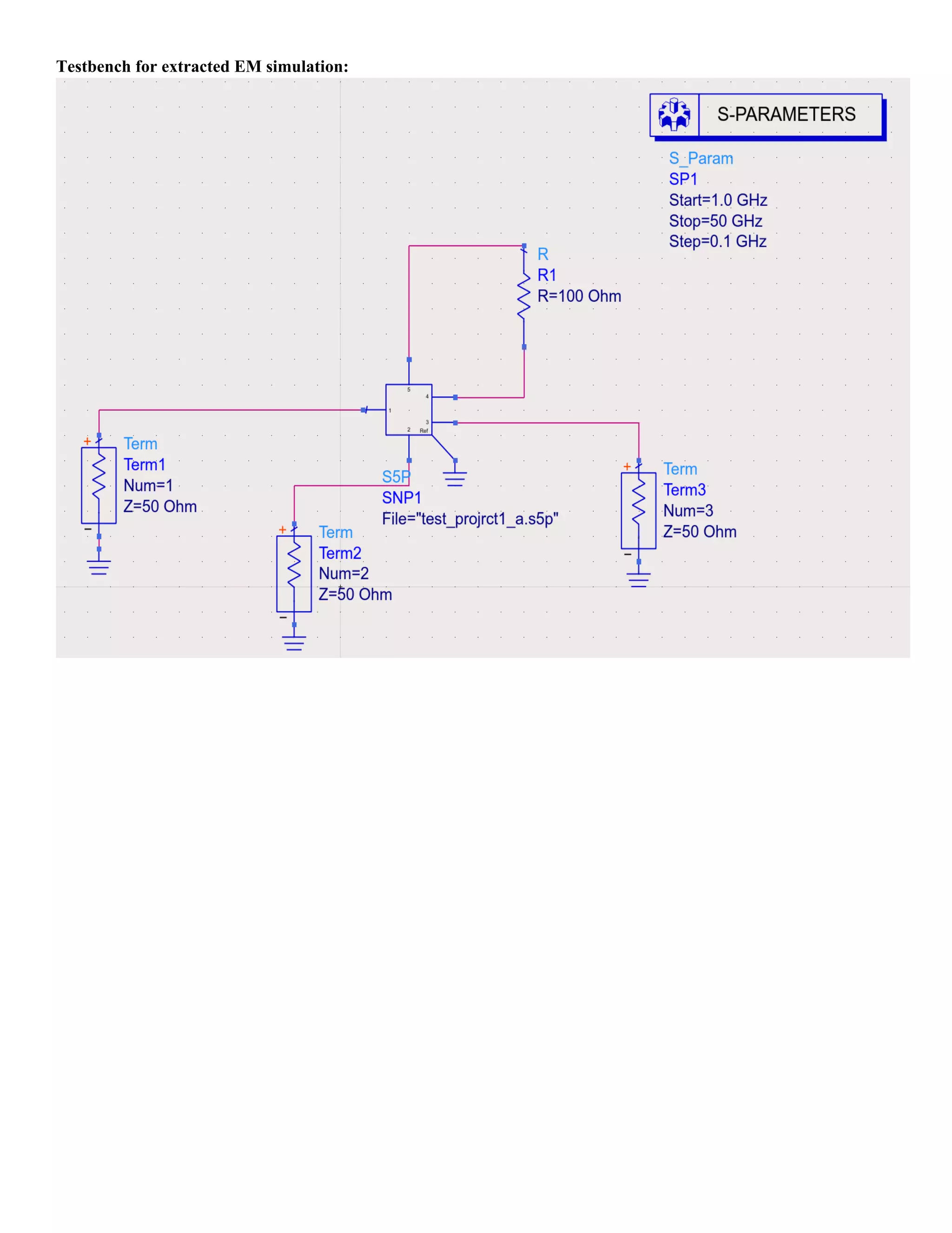
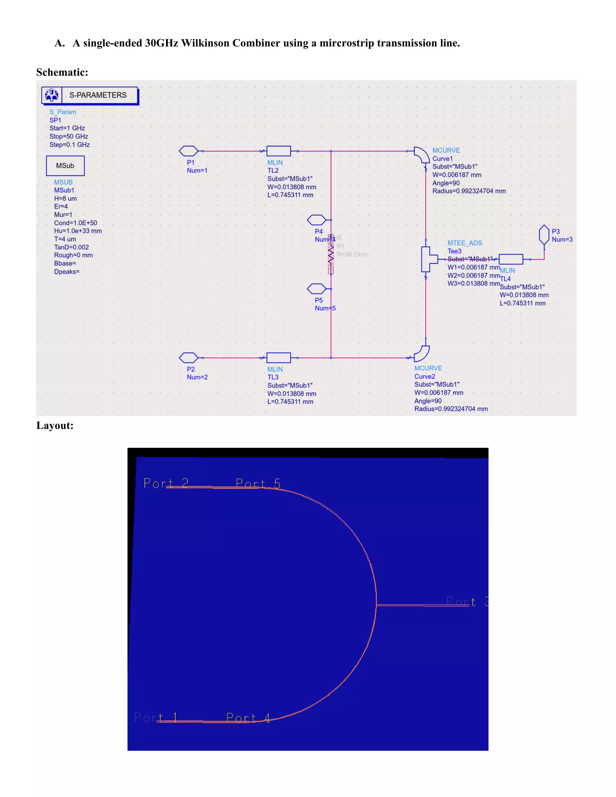
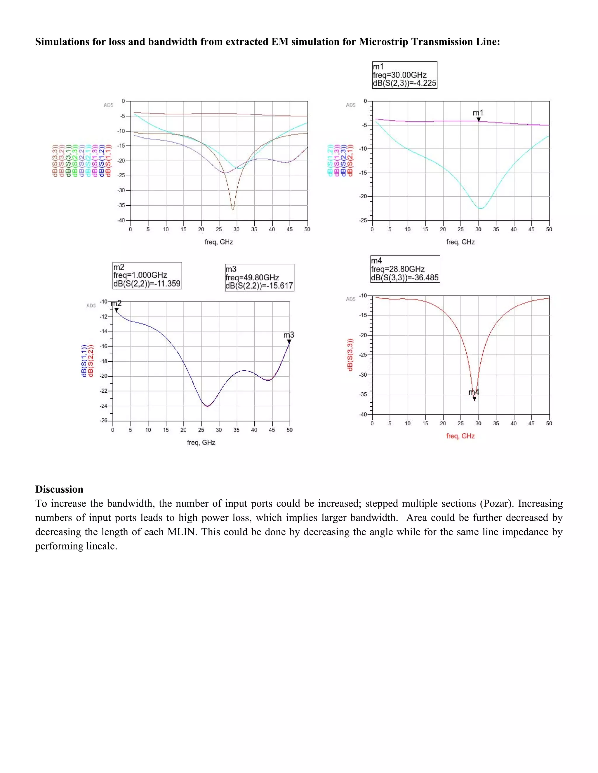
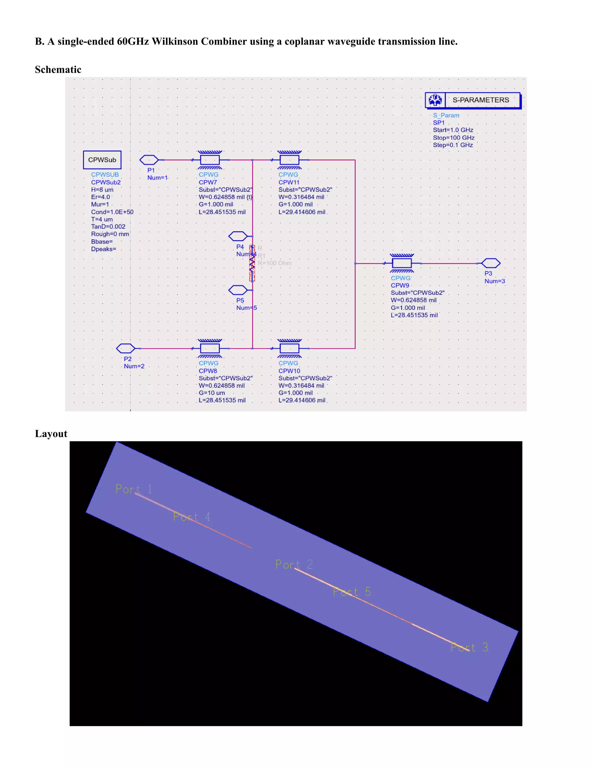
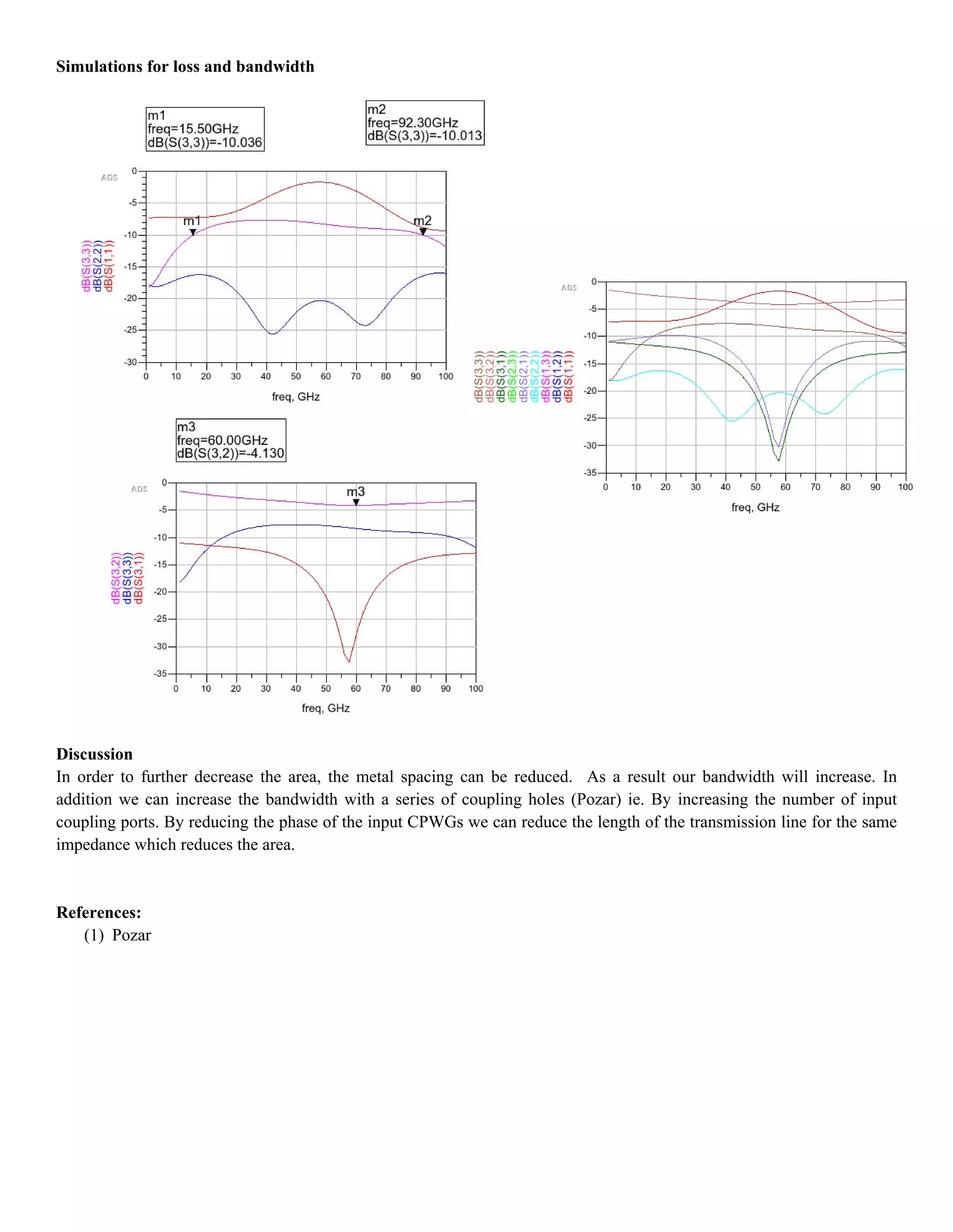

This report details the design and layout of a Wilkinson combiner using microstrip transmission line and coplanar waveguide. It demonstrates how to achieve optimal power division with specific impedance requirements and discusses the simulation results, including bandwidth and power loss calculations. Recommendations for increasing bandwidth and reducing area through design adjustments are also provided.


