This document discusses the design and simulation of a high-speed CMOS differential current sensing comparator in 0.35μm and 0.25μm technologies. It presents the circuit design of the differential current sensing comparator and output buffer stage. Various performance metrics of the comparator like propagation delay, speed, power dissipation, offset voltage, and input common mode range are analyzed through simulations in the two technologies. The results show improvements in speed, power dissipation, and input common mode range in the 0.25μm technology compared to the 0.35μm technology.
![INTERNATIONAL JOURNAL OF ELECTRONICS AND
International Journal of Electronics and Communication Engineering & Technology (IJECET), ISSN
COMMUNICATION ENGINEERING & TECHNOLOGY (IJECET)
0976 – 6464(Print), ISSN 0976 – 6472(Online) Volume 3, Issue 3, October- December (2012), © IAEME
ISSN 0976 – 6464(Print)
ISSN 0976 – 6472(Online)
Volume 3, Issue 3, October- December (2012), pp. 147-152
IJECET
© IAEME: www.iaeme.com/ijecet.asp
Journal Impact Factor (2012): 3.5930 (Calculated by GISI) ©IAEME
www.jifactor.com
DESIGN AND SIMULATION OF HIGH SPEED CMOS DIFFERENTIAL
CURRENT SENSING COMPARATOR IN 0.35µm AND 0.25µm
TECHNOLOGIES
Dhanisha N. Kapadia1, Priyesh P. Gandhi2
1
(E.C.Dept, L.C. Institute of Technology, Bhandu, INDIA,dhally_007@yahoo.co.in)
2
(E.C.Dept, L.C. Institute of Technology, Bhandu, INDIA,priyesh.gandhi@lcit.org)
ABSTRACT
This paper presents various analysis of different characteristics of Differential current sensing
comparator along with the buffer stage. Different characteristics of comparator such as propagation
delay, speed, power dissipation, input common mode range, offset has been carried out in two
different technologies 0.35um and 0.25um . The supply voltage is kept at 3v, 2.5v for 0.35um and
0.25um respectively.
Keywords: ADC, Buffer, Latch comparator, Current sensing comparator.
I. INTRODUCTION
A comparator can be defined as the circuit that compares one analog signal with another
analog signal or reference signal and gives the output in binary form as either logic’0’ or
logic’1’ based on the comparison. The application of the comparator lies in ADC, memory
sensing elements etc. Mostly, it is widely used in analog to digital converters. It is also
known as 1bit ADC. For designing any comparators various specifications needs to be
considered such as propagation delay, speed, power dissipation, offset voltage, input
common mode range. The main advantage of using dynamic latch comparator is the
reduction of silicon are on the chip by replacing traditional preamplifiers [1][2].Another
advantage of dynamic latch comparator lies in less power dissipation as compared to
preamplifiers stage based comparators. This paper is focused on Differential current
sensing comparator which is a dynamic latch comparator.
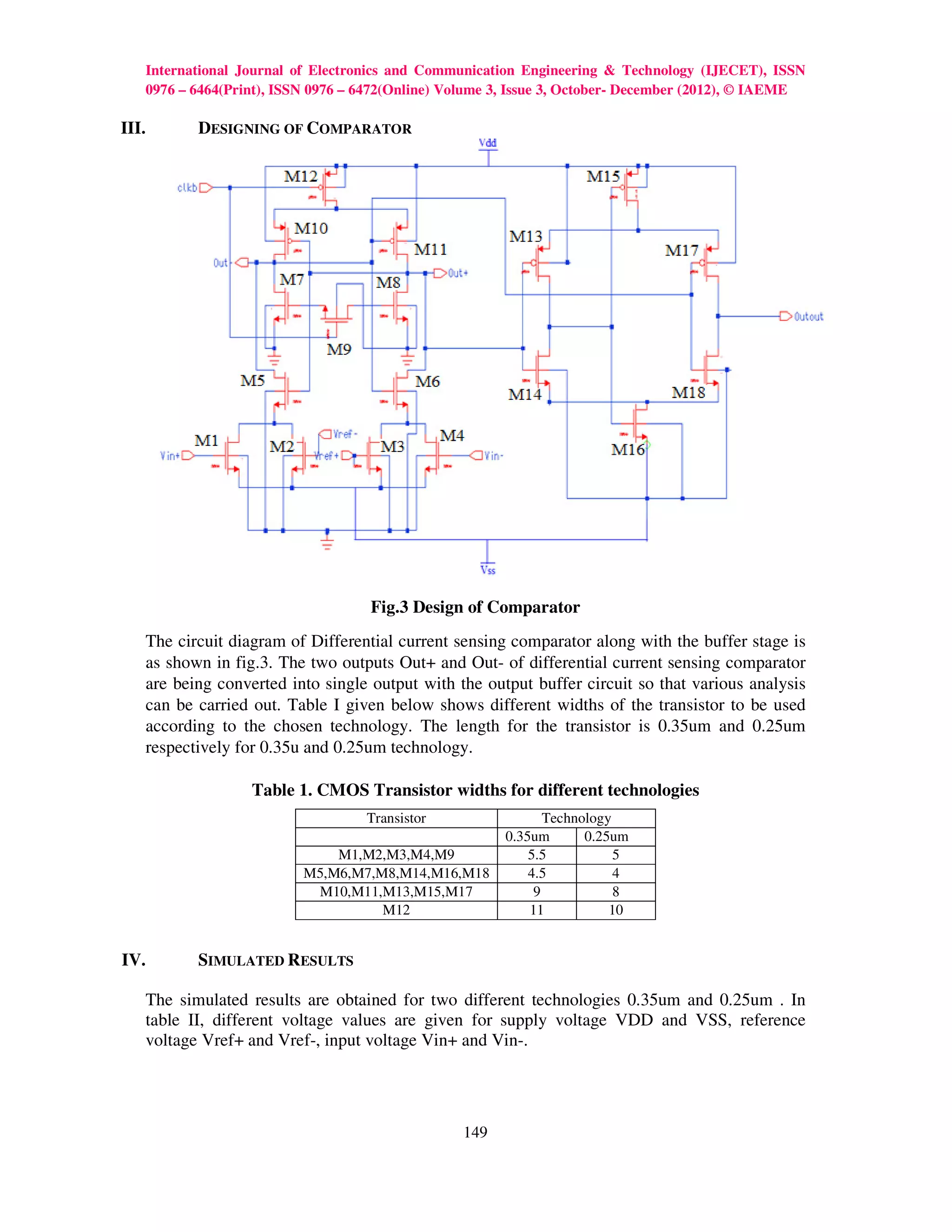
II. DIFFERENTIAL CURRENT SENSING COMPARATOR AND BUFFER STAGE
2.1 Differential Current Sensing Comparator
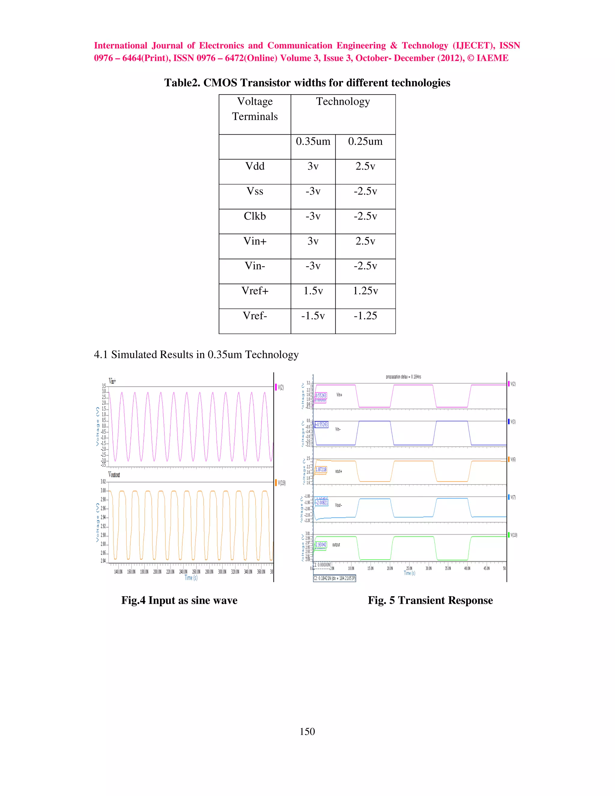
The schematic of the differential current sensing comparator is as shown in fig.1. Whenever
the Clk signal goes low, the circuit enters in regenerative mode. Transistor M12 is on and M7
is off. When values of both the outputs Out+ and Out- increases above threshold voltage of
147](https://image.slidesharecdn.com/designandsimulationofhighspeedcmos-121220235237-phpapp01/75/Design-and-simulation-of-high-speed-cmos-1-2048.jpg)
![International Journal of Electronics and Communication Engineering & Technology (IJECET), ISSN
0976 – 6464(Print), ISSN 0976 – 6472(Online) Volume 3, Issue 3, October- December (2012), © IAEME
nMOS M5 and M6, both will start conducting which will connect the outputs with comparing
circuit at the input side. It consumes more power because unless and until final state is
reached both the outputs have to drive common mode currents.
The comparing circuit used at the input side consisting of transistors M1, M2, M3 and M4
are used to transfer the difference of the input voltage into differential currents. During reset
interval, a pass transistor M7 is used to connect both the outputs together
Fig. 1. Differential current sensing comparator[3]
2.2 The Buffer Stage
Fig.2 The Output Buffer Circuit [4]
The schematic of output buffer circuit used in the comparator is shown in figure 2[4]. The
output buffer stage is also known as post amplifier. This circuit is self biasing differential
amplifier which has differential inputs as Vout+ & Vout- and does not have any slew rate
limitations. It is also useful in giving the output in proper shape.
148](https://image.slidesharecdn.com/designandsimulationofhighspeedcmos-121220235237-phpapp01/75/Design-and-simulation-of-high-speed-cmos-2-2048.jpg)
![International Journal of Electronics and Communication Engineering & Technology (IJECET), ISSN
0976 – 6464(Print), ISSN 0976 – 6472(Online) Volume 3, Issue 3, October- December (2012), © IAEME
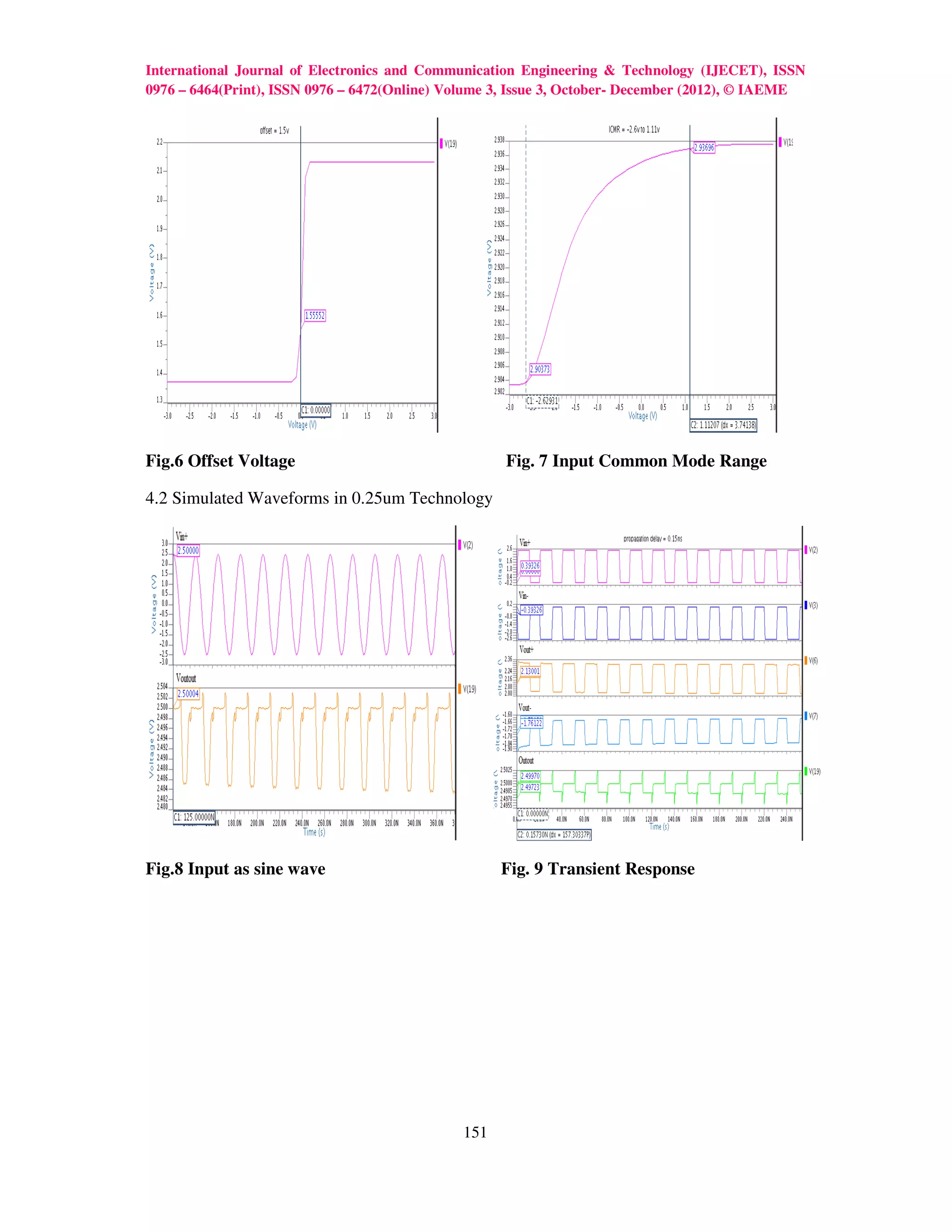
Fig. 10 Offset Voltage Fig. 11 Input Common Mode Range
V. CONCLUSION
In this paper, simulated results are presented for the comparator for two different
technologies, 0.35um and 0.25unm. The summary of the comparison for the Differential
current sensing comparator in both the technologies is given in the table III.
TABLE III Different measured parameter values for different Technologies
Parameters Technology
0.35um 0.25um
Propagation Delay(ns) 0.184 0.15
Speed(GHz) 5.43 6.67
Offset(v) 1.55 1.59
ICMR(v) -2.6 to 1.11 -2.26 to
0.09
Power Dissipation(mV) 20.6 12.6
REFERENCES
[1] P. Uthaichana and E. Leelarasmee, "Low Power CMOS Dynamic Latch Comparators,"
IEEE, pp. 605-608, 2003.
[2] Z. Huang and P. Zhong, "An Adaptive Analog-to-Digital Converter Based on Low-Power
Dynamic Latch Comparator," IEEE conference, p. 6pp, 2005.
[3] Christopher J. Lindsley “A Nano-Power Wake-Up Circuit for RF Energy Harvesting
Wireless Sensor Networks” , M.S. thesis, Dept. Electrical & computer. Eng., Oregon
State University 2008.
[4] Priyesh P. Gandhi “Design & Simulation of Low Power High Speed CMOS Comparator
in Deep Sub-micron Technology”, M.Tech thesis, Dept. of electronics & communication
Eng. Nirma University, 2010.
152](https://image.slidesharecdn.com/designandsimulationofhighspeedcmos-121220235237-phpapp01/75/Design-and-simulation-of-high-speed-cmos-6-2048.jpg)


![Analysis and design_of_a_low-voltage_low-power[1]](https://cdn.slidesharecdn.com/ss_thumbnails/analysisanddesignofalow-voltagelow-power1-140802050345-phpapp02-thumbnail.jpg?width=640&height=640&fit=bounds)