Downloaded 223 times
![P a g e | 17
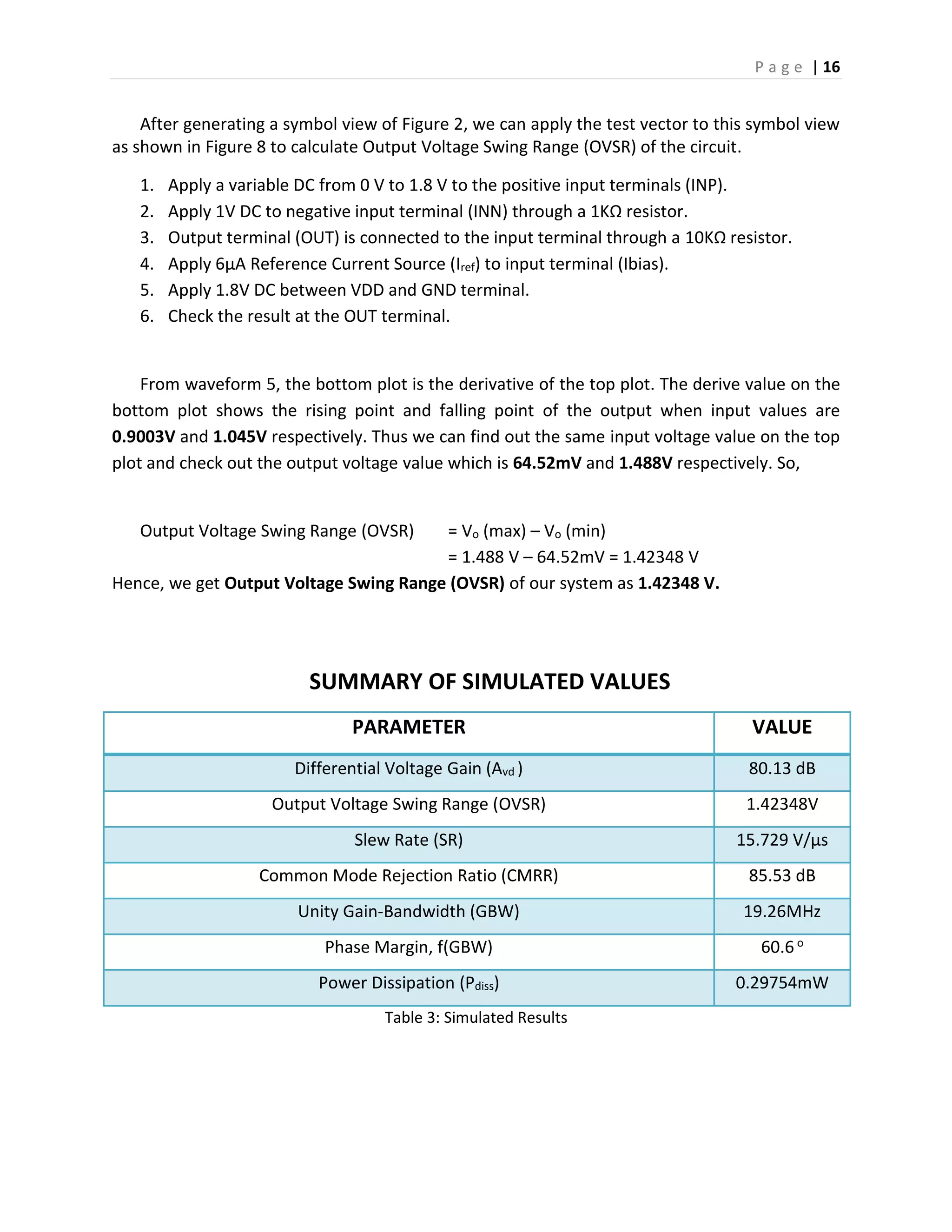
FINAL SCORE
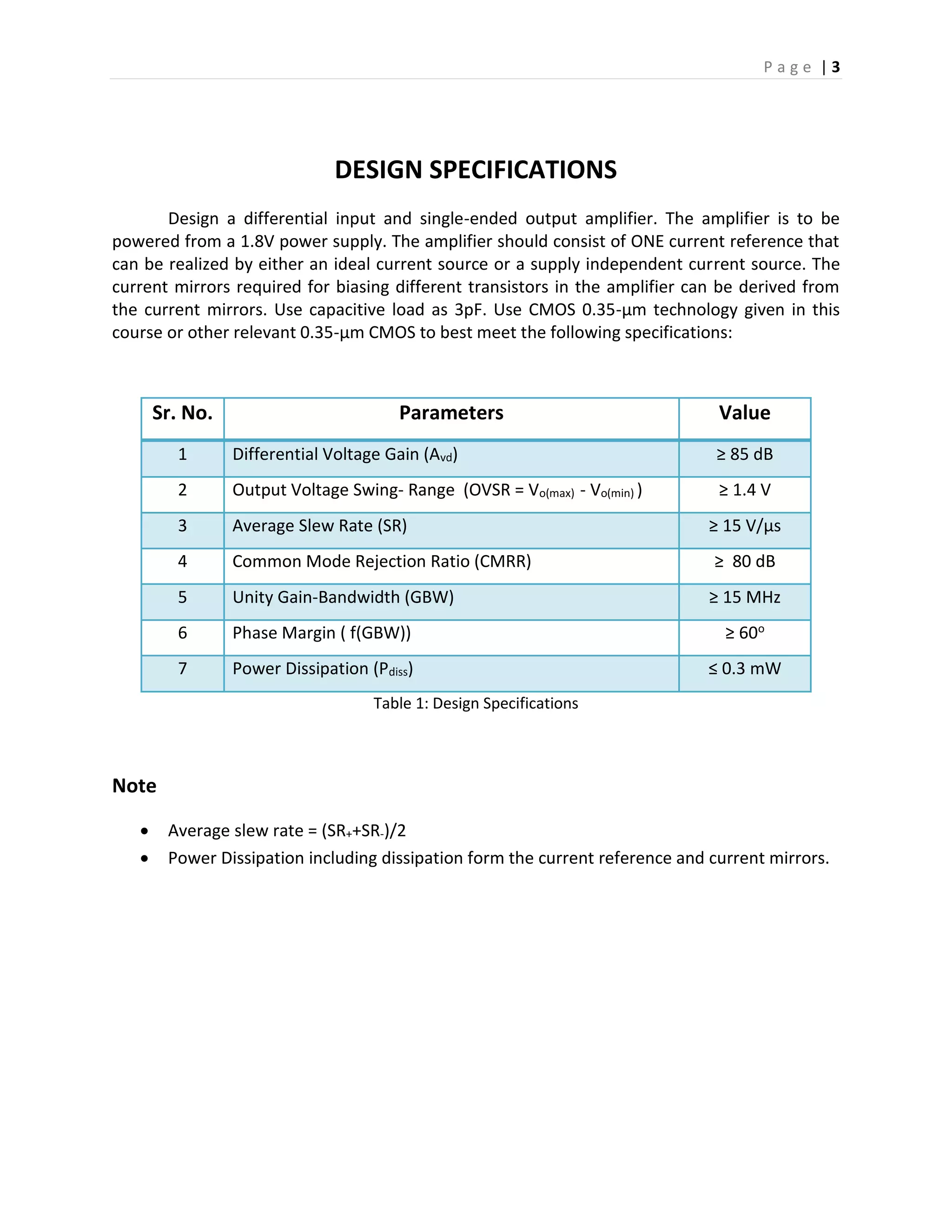
Avd(dB) OVSR(V) SR(V/µs) CMRR(dB) GBW(MHz) PM(deg) Pdiss(mW)
Required ≥ 85 dB ≥ 1.4 V ≥ 15 V/µs ≥ 80 dB ≥ 15 MHz ≥ 60o ≤ 0.3mW
Actual 80.13 dB 1.42348V 15.729 V/µs 85.53 dB 19.26MHz 60.6 o 0.29754mW
Score 14.14 10 20 10 20 10 15
Table 4: Final Score for individual parameters
Score Formula = min[15,15(
𝐴𝑣𝑑
85𝑑𝐵
)] + min[10,10(
𝑂𝑉𝑆𝑅
1.4𝑉
)] + min[20,20(
𝑆𝑅
15𝑉/𝑢𝑠
)] +
min[10,10(
𝐶𝑀𝑅𝑅
80𝑑𝐵
)] + min[20,20(
𝐺𝐵𝑊
15𝑀𝐻𝑧
)] + min[10,10(
𝑃𝑀
60
)] + min[15,15(
0.3𝑚𝑊
𝑃𝑑𝑖𝑠𝑠
)]
Final Score = 99.14
CONCLUSION
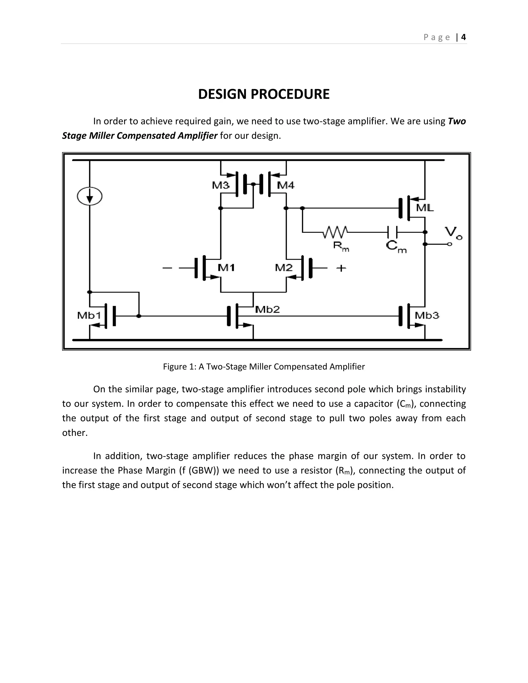
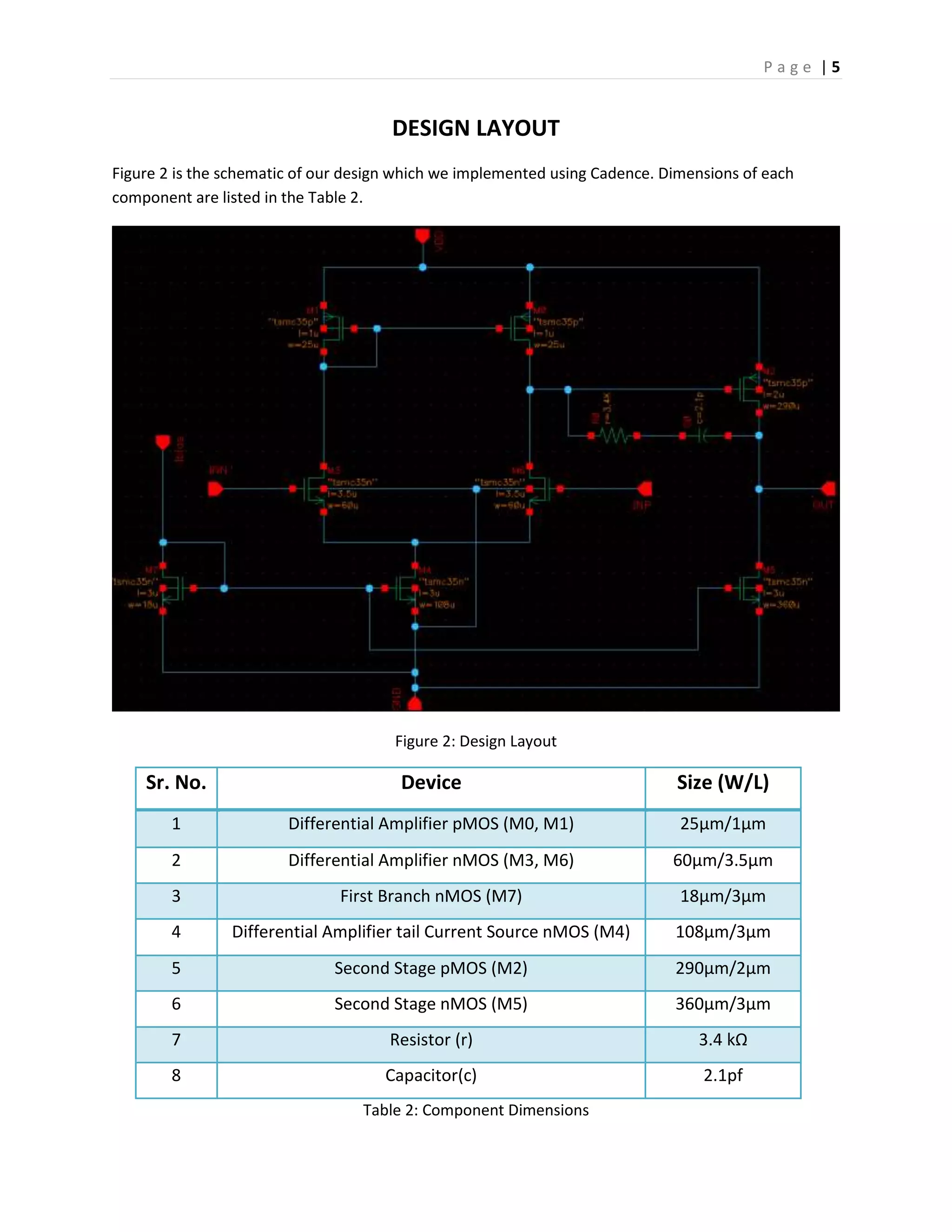
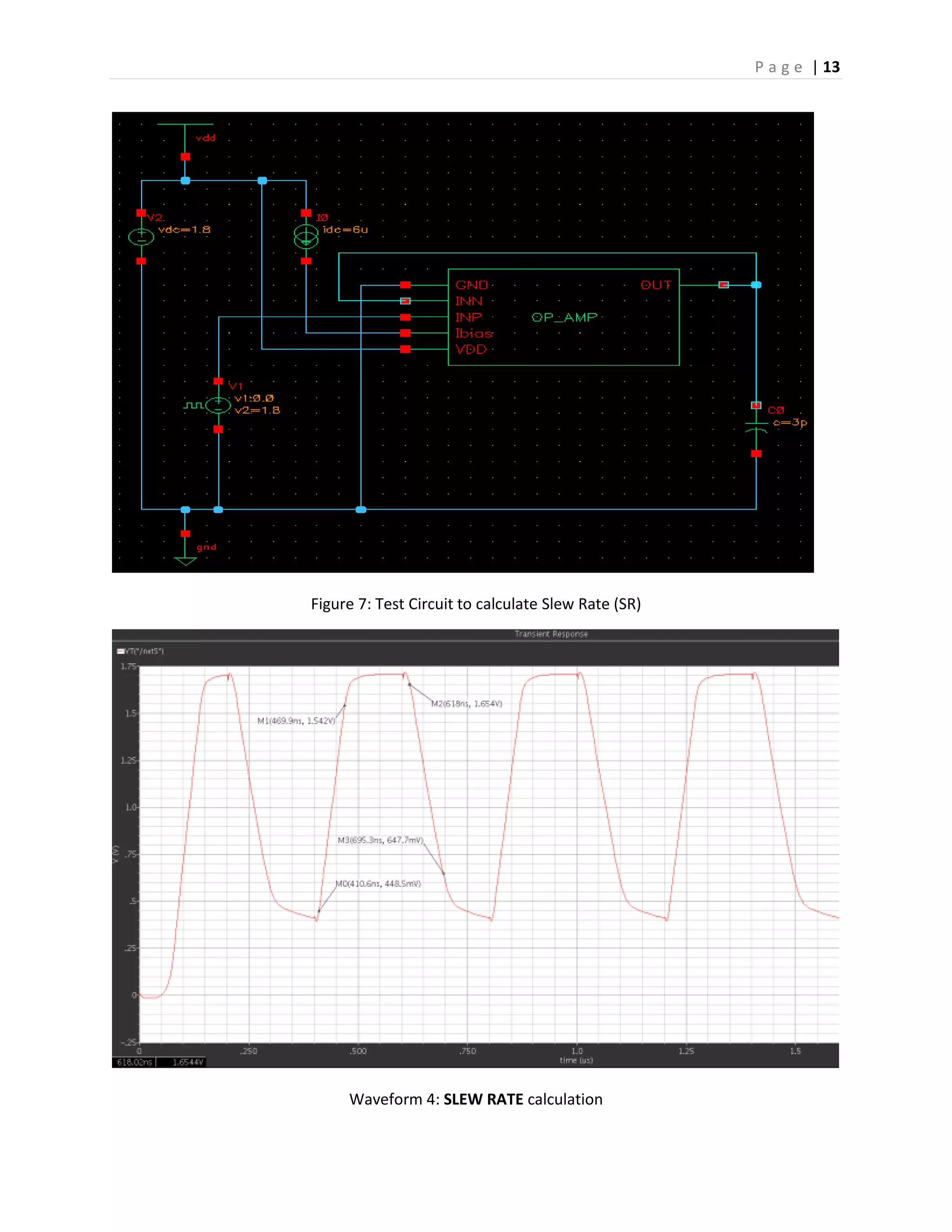
The developed Operational Amplifier using “Two-Stage Compensated Amplifier” design
met all the specifications except Gain. The gain has been sacrificed to avoid huge sizing of the
transistors.
REFERENCES
[1] B. Razavi, Design of Analog CMOS Integrated Circuits, New York: Tata-McGraw Hill, 2002.
[2] H. Lee, Class notes, EE6326 – Spring 2014, University of Texas, Dallas, 2014](https://image.slidesharecdn.com/operationalamplifierdesignanalogicdesign3rdmay2014-140610005558-phpapp01/75/Operational-Amplifier-Design-17-2048.jpg)

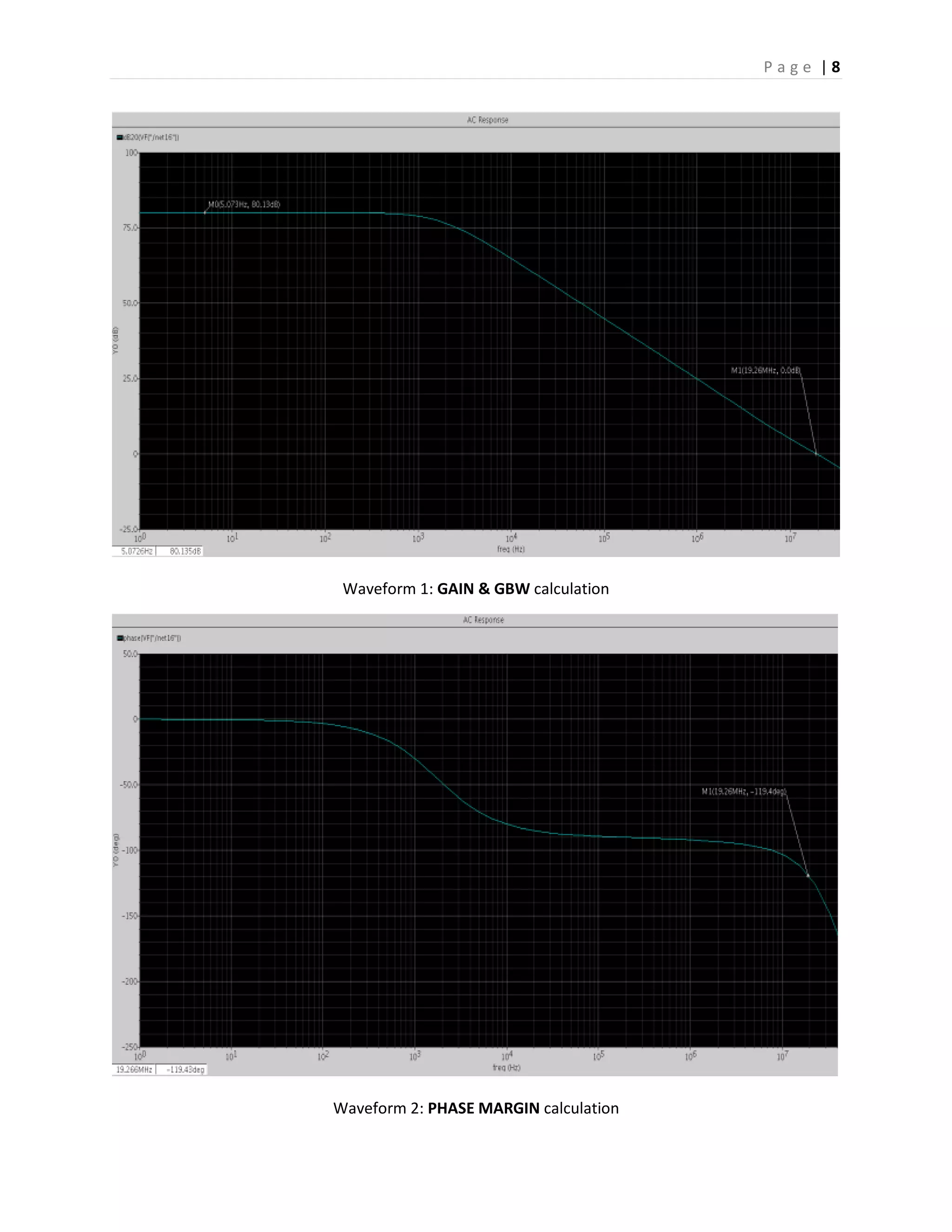
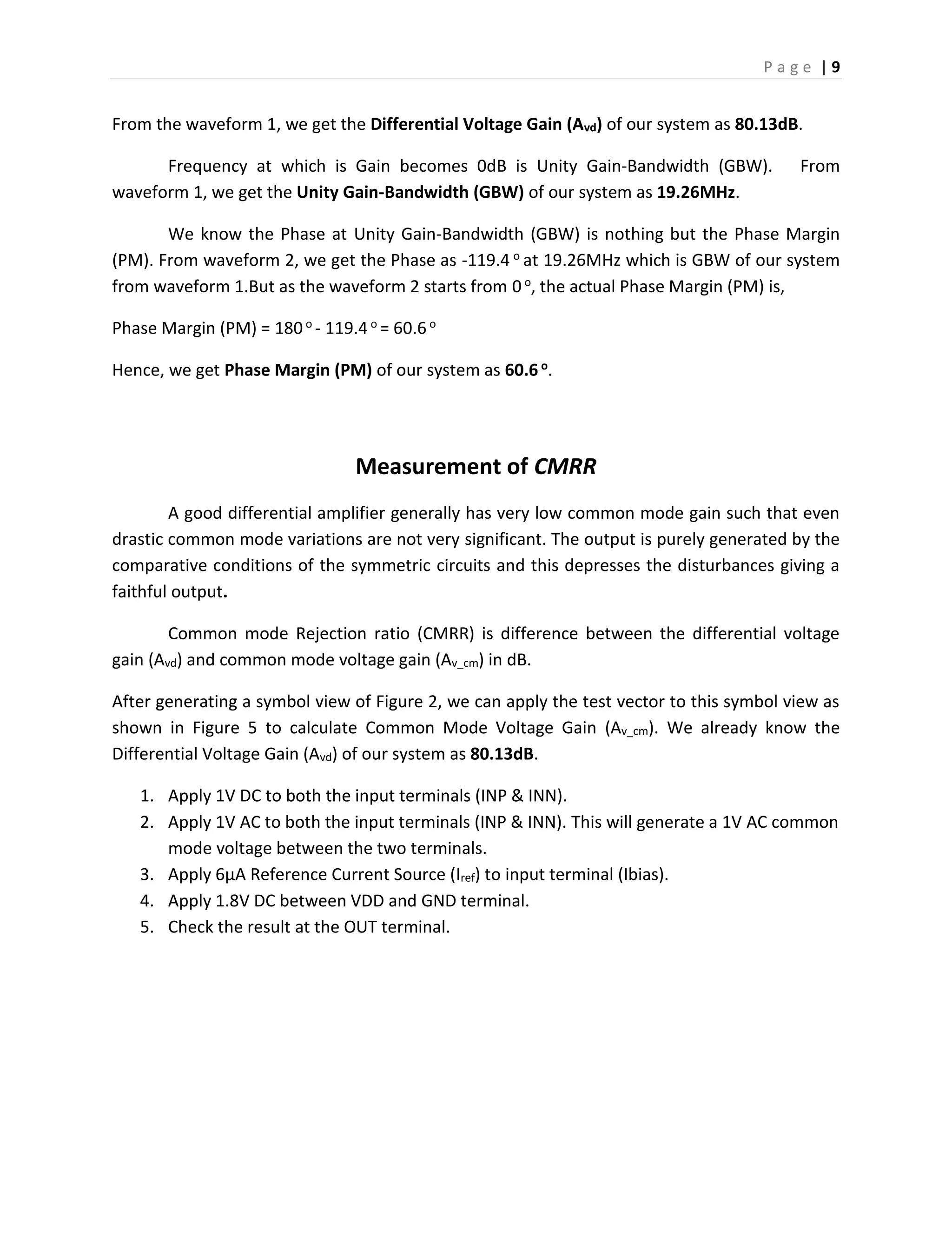
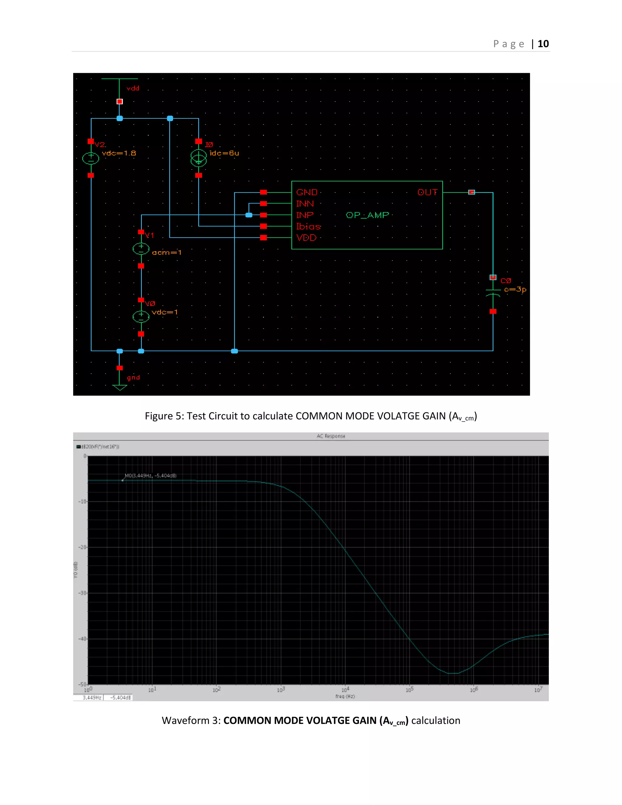
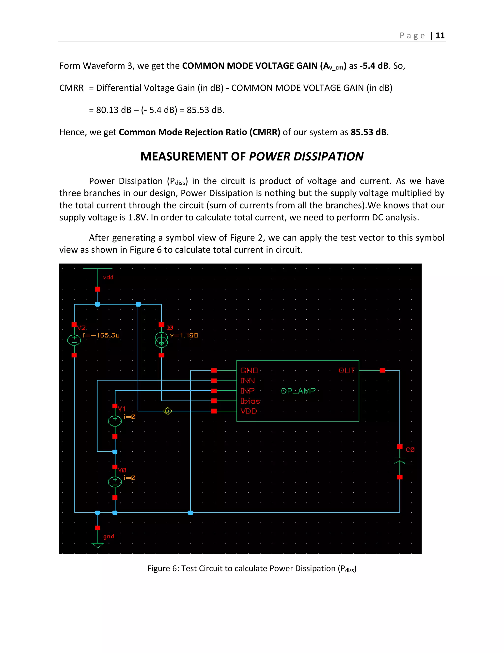
The document outlines the design and testing of a differential operational amplifier, including specifications, procedures, and measurements of various parameters such as gain, output voltage swing range, and common mode rejection ratio. It details the design process using a two-stage Miller compensated amplifier and provides simulated results that meet most required specifications, though the differential voltage gain fell slightly short. Conclusions indicate that while the amplifier successfully met most specifications, the gain was compromised to manage transistor sizing.