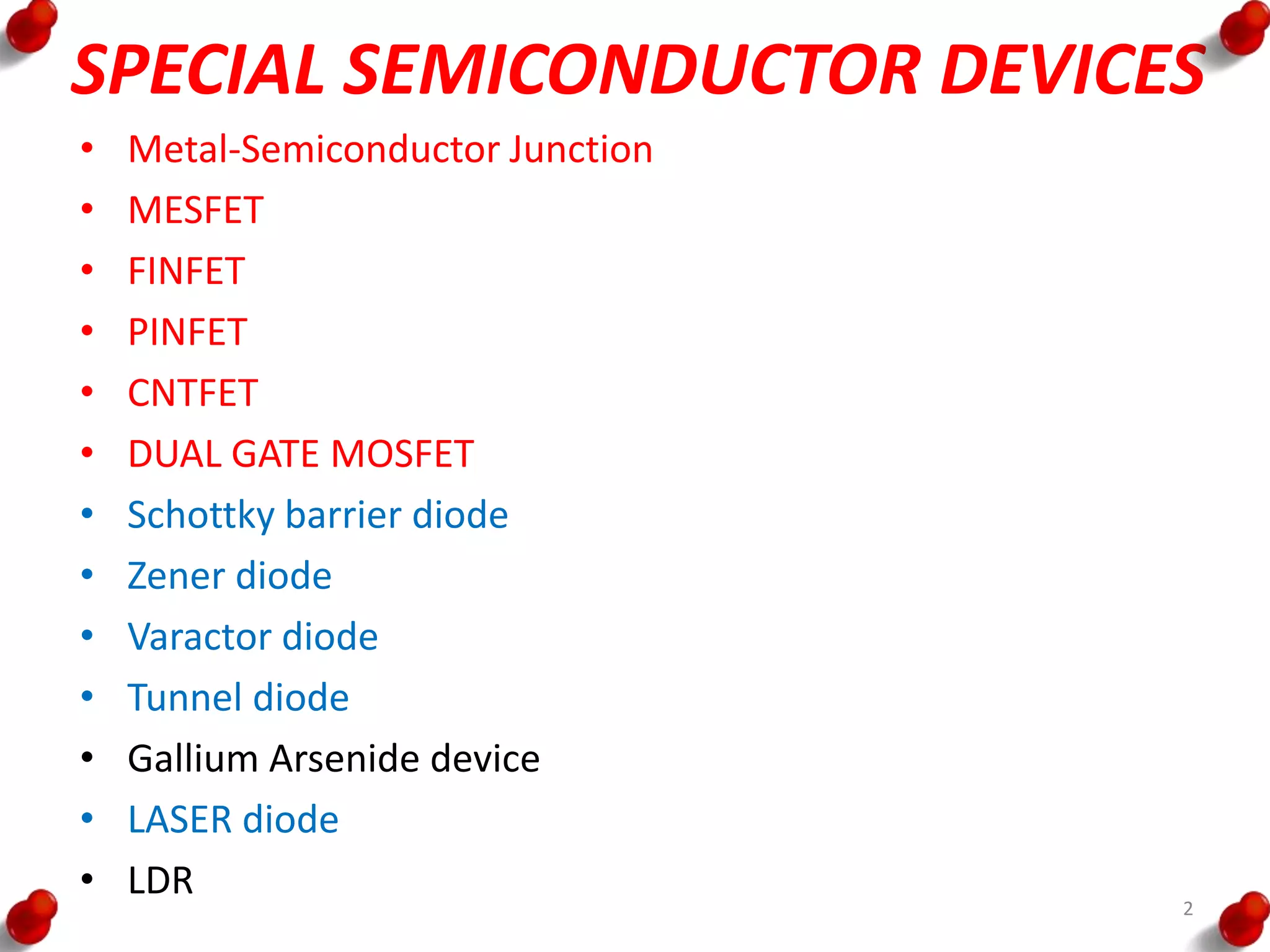
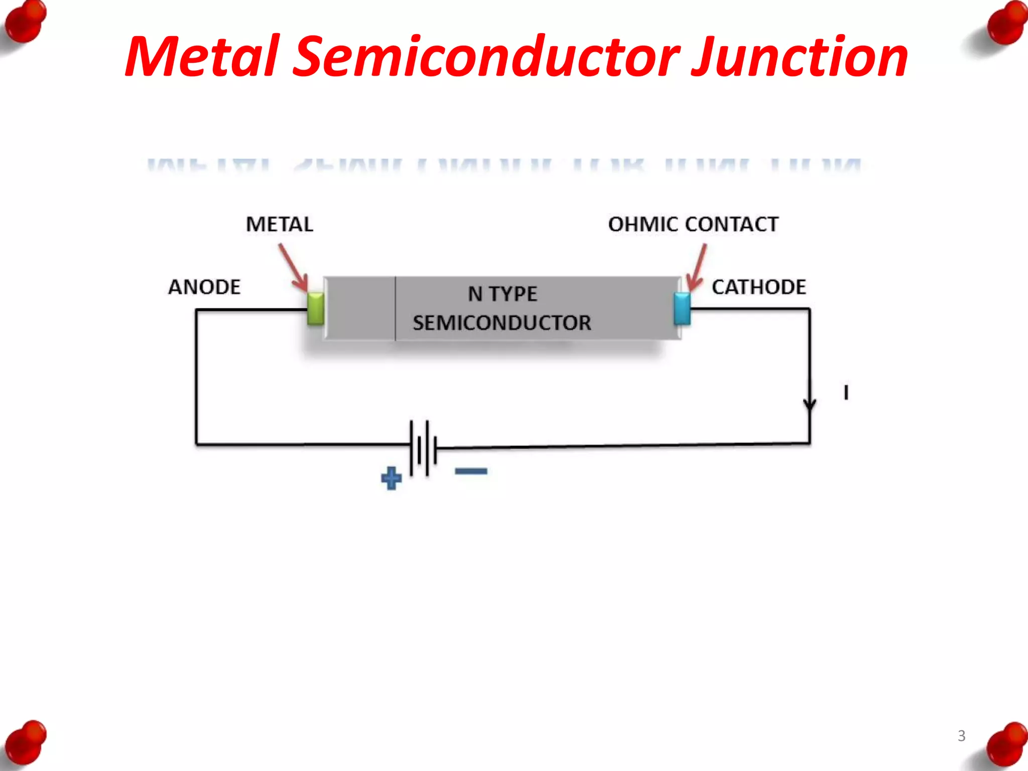
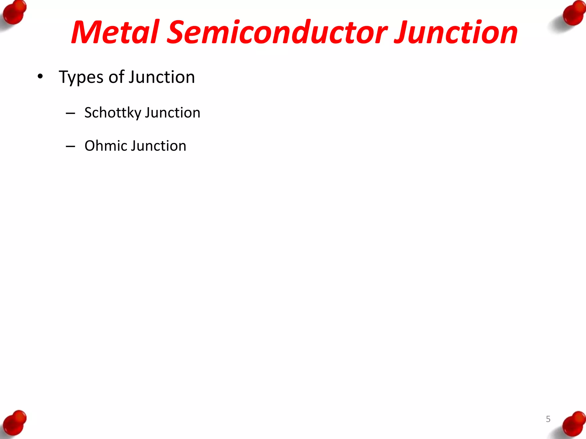
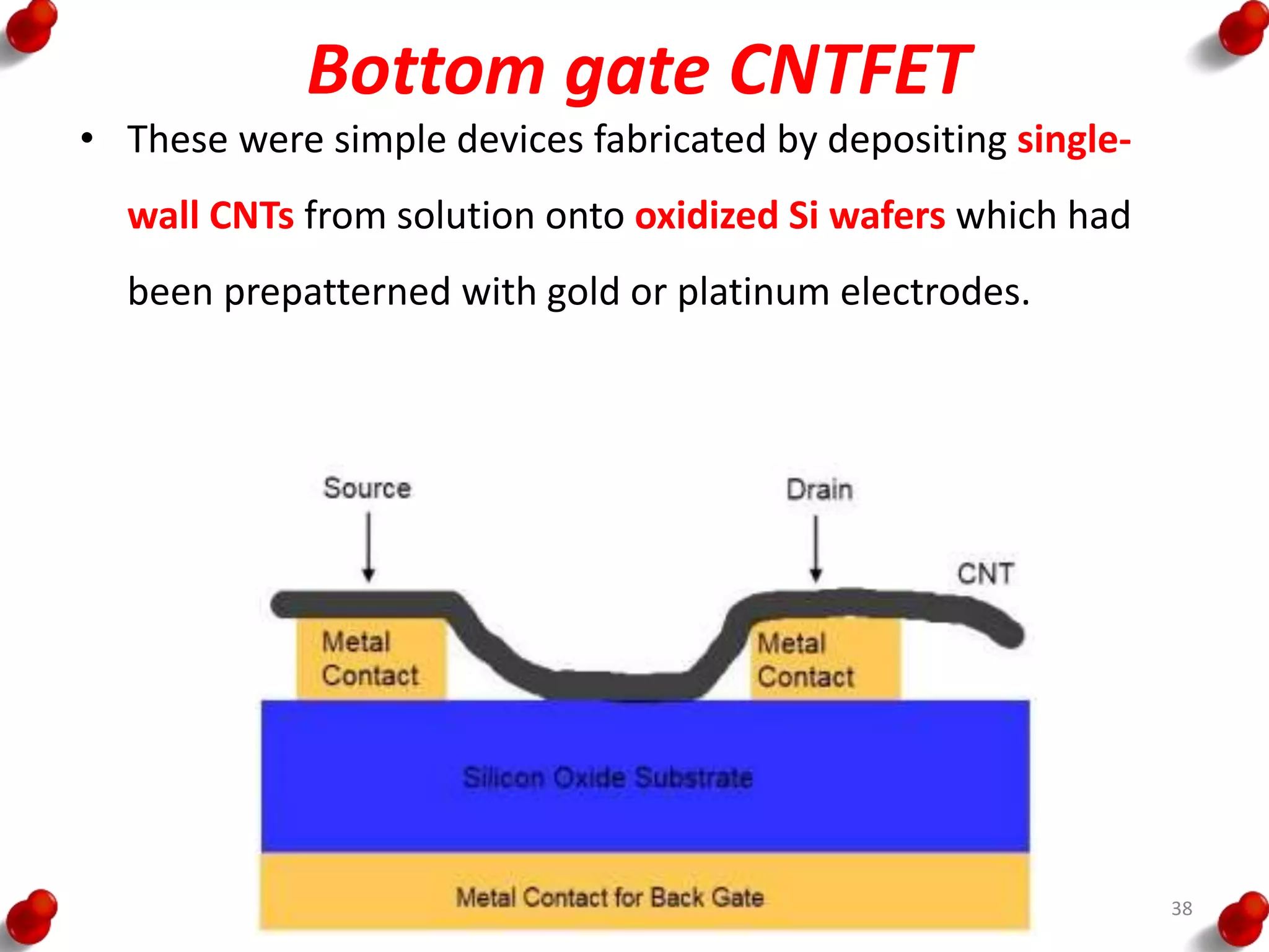
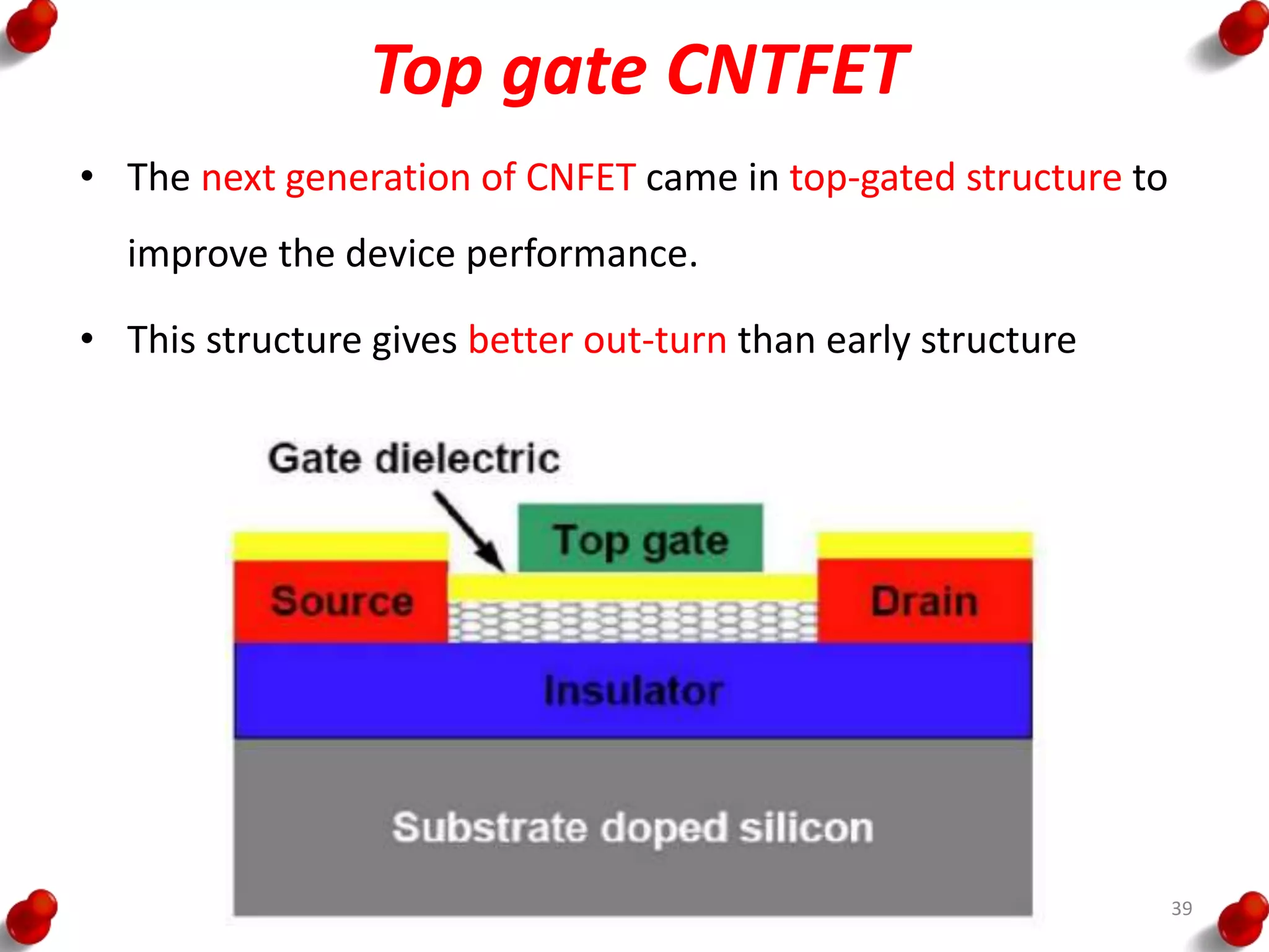
SPECIAL SEMICONDUCTOR
DEVICES
T.Ramprakash
AP/ECE
Ramco Institute of Technology
Rajapalayam
1
SPECIAL SEMICONDUCTOR DEVICES
• Metal-Semiconductor Junction
• MESFET
• FINFET
• PINFET
• CNTFET
• DUAL GATE MOSFET
• Schottky barrier diode
• Zener diode
• Varactor diode
• Tunnel diode
• Gallium Arsenide device
• LASER diode
• LDR
2
Metal Semiconductor Junction
3
Metal Semiconductor Junction
4
Metal Semiconductor Junction
• Types of Junction
– Schottky Junction
– Ohmic Junction
5
Schottky Junction
6
Schottky Junction under forward bias and
reverse bias
7
Schottky Junction V-I Characteristics
8
Ohmic Junction
9
Ohmic Junction V-I Characterisitics
10
MESFET
• Two advantages of using GaAs that silicon
– Electron mobility at room temperature is more than 5 times large and
peak electron velocity is about twice that of silicon
– It eliminates the problem of absorbing microwave power in the
substrate due to free carrier absorption and provides better operation
at high temperature 11
MESFET
• METAL SEMICONDUCTOR FIELD EFFECT TRANSISTORS
• It is also called as Schottky gate FET
• MESFET consists of a conducting channel positioned between
a source and drain contact region.
• The carrier flow from source to drain is controlled by a
Schottky metal gate
• The control of the channel is obtained by varying the
depletion layer width underneath the metal contact which
modulates the thickness of the conducting channel and
thereby the current. 12
MESFET
13
MESFET
• The key advantage of the MESFET is the higher mobility of the
carriers in the channel as compared to the MOSFET.
• GaAs MESFETs are the most commonly used and important
active devices in microwave circuits.
• MESFET is the dominant active device for
– power amplifiers and
– switching circuits in the microwave spectrum.
14
Construction of MESFET
15
Construction of MESFET
• The base material on which the transistor is fabricated is a
GaAs substrate.
• A buffer layer is epitaxially grown over the GaAs substrate to
isolate defects in the substrate from the transistor.
• The channel or the conducting layer is a thin, lightly doped (n)
conducting layer of semiconducting material epitaxially grown
over the buffer layer.
16
Construction of MESFET
• Finally, a highly doped (n+) layer is grown on the surface to aid
in the fabrication of low-resistance ohmic contacts to the
transistor.
• This layer is etched away in the channel region.
• Two ohmic contacts, the source and drain, are fabricated on
the highly doped layer to provide access to the external
circuit.
• Between the two ohmic contacts, a rectifying or Schottky
contact is fabricated.
17
MESFET - Applications
• MESFET applications:
– High frequency devices,
– cellular phones,
– Satellite receivers,
– radar,
– microwave devices.
• GaAs is a primary material for MESFETs.
• GaAs has high electron mobility.
• Generally,
– if f > 2 GHz: GaAs transistors are usually used.
– If f < 2 GHz: Si transistors are usually used.
18
MESFET - Applications
MOSFET MESFET
Gate is controlled through a MOS barrier Gate control takes place through a Schottky
barrier
MOSFET are usually fabricated in Si MESFET are usually fabricated in GaAs
MOSFET is normally in OFF state and there
is a flow of current only when the channel
is inverted by gate bias
MESFET is normally in ON state and
negative gate bias is needed to turn the
current to OFF state
Both P-channel and N-channel MOSFET are
possible giving rise to CMOS
Typically N-channel MESFET are feasible
MOSFET is mainly in integrated circuits, but
microwave operation is not yet possible.
MESFET is mainly used in microwave
devices but the integration level is not as
high as the CMOS devices
19
FINFET• FinFET, also known as Fin Field Effect Transistor
• FinFET is designed to address performance shortcomings due to
short channel effects
• It is overcome by wrapping the gate around the conduction
channel instead of having it laid on the top of transistor
20
FINFET
• It is a type of non-planar or "3D" transistor used in the design of
modern processors.
• It is built on an SOI (silicon on insulator) substrate.
• However, FinFET designs also use a conducting channel that rises
above the level of the insulator, creating a thin silicon structure,
shaped like a fin, which is called a gate electrode.
• This fin-shaped electrode allows multiple gates to operate on a
single transistor.
21
FINFET
• Short Channel Effects can be reduced by sandwiching a fully
depleted SOI device between two gate electrodes connected
together.
• First FINFET - Double gate SOI MOSFET was the fully DEpleted
Lean-channel TrAnsistor(DELTA).
22
FINFET
23
FINFET
24
FINFET
• Applications
– TO construct Low Power Logic Gates
– Single Transistor Mixer
– SRAMs
25
FINFET
• Advantages
– Provides better electrostatic control over the channel
– Reduces the short channel effects
– Excellent control of short channel effects makes transistors still
scalable
– Much lower leakage current
• Applications
– To construct Low Power Logic Gates
– Single Transistor Mixer
– SRAMs
26
PINFET
• PINFET – (P-Intrinsic N Field Effect Transistor)
• It is a combination of PIN photodiode and FET in a single
housing
• It is mainly used as
– Low noise
– High speed photo receiver in optical communication
• PIN-FET has wide dynamic range and increased sensitivity.
27
PINFET• The PIN diode is a one type of photo detector, used to convert
optical signal into an electrical signal.
• The PIN diode comprises of three regions, namely
– P-region,
– I-region and
– N-region.
• Typically, both the P and N regions are heavily doped due to
they are utilized for Ohmic contacts.
• It is reverse biased junction diode
• A layer of intrinsic silicon is sandwiched between heavily
doped P and N type semiconductor material 28
PINFET
• The intrinsic layer is wider and it is the absorption of light
photons
• Light photons absorbed in the intrinsic region leads to the
generation of electron hole pairs
• Thus the reverse current flow in the external circuit linearly
increases with the level of illumination.
29
PINFET Construction
• A monolithic PIN FET optical receiver is fabricated on a semi
insulating InGaAs substrate by using Metal-Organic Chemical
Vapour Deposition (MOCVD)
N + InP Substrate
N – InGaAS
S.I.-InPP
N
N+ P
PIN Diode ION Implanted JFET
30
PINFET Construction
• The PIN-FET is an integration of
InGaAs PIN Photodiode and
InGaAs FET.
• The material is grown on N+InP
substrate
• The InGaAs layer of low electron
concentration is grown on the
InP by chloride vapour phase
epitaxy (VPE)
N + InP Substrate
N – InGaAS
S.I.-InPP
N N+ P
PIN Diode ION Implanted JFET
• The second growth is done by atmospheric pressure metal organic
chemical vapour deposition(MOCVD) technique
31
PINFET Construction
• Then it is subjected to series of
ion implantations to form the
FET
• After the deposition of
passivation layer, the diffusion of
Zn is performed to form the PIN
diode
• The resulting PIN junction is
located near the InP-InGaAs
interface
N + InP Substrate
N – InGaAS
S.I.-InPP
N N+ P
PIN Diode ION Implanted JFET
32
CNTFET
33
CNTFET
34
CNTFET
• CNTFET – Carbon Nanotube Field Effect Transistors
• One major difference between CNTFET and MOSFET is that
the channel of the device is formed by Carbon Nano
Tubes(CNTs) instead of silicon
• CNT enables a higher drive current density
35
CNTFET• Carbon nanotubes (CNTs) were discovered by Ijima in Japan
in 1991
• CNT is a cylindrical shaped nanostructure, made of allotropes
of carbon
• CNTs can be thought as rolled up sheets of graphene
36
CNTFET - Types
• Based on geometry
– Top Gate
– Bottom Gate
– Coaxial Gate
• Based on operation
– Schottky barrier
– MOSFET
37
Bottom gate CNTFET
• These were simple devices fabricated by depositing single-
wall CNTs from solution onto oxidized Si wafers which had
been prepatterned with gold or platinum electrodes.
38
Top gate CNTFET
• The next generation of CNFET came in top-gated structure to
improve the device performance.
• This structure gives better out-turn than early structure
39
Coaxial gate CNTFET
• Gate all around geometry.
• More electrostatic control over channel
40
Working Principle of CNTFET
• Basic principle operation of CNFET is the same as MOSFET
where electrons are supplied by source terminal and drain
terminal will collect these electrons .
• In other words, current is actually flowing from drain to
source terminal .
• Gate terminal controls current intensity in the transistor
channel and the transistor is in off state if no gate voltage is
applied.
41
DUAL GATE MOSFET
• The operation of MOSFET is limited at high frequencies by its
high gate to channel capacitance
• A dual gate MOSFET uses two gates to reduce the overall high
gate-to-channel capacitance at high frequencies.
42
DUAL GATE MOSFET
43
DUAL GATE MOSFET
44
DUAL GATE MOSFET
• The second gate is typically operated at fixed voltage to keep
feedback capacitance between drain and gate small.
• The voltage applied on the gate terminals controls the electric
fields, determining the amount of current flow through the
channel.
45
Applications
• Advantages:
– Reduction of short channel effects.
– Maintaining good electrical characteristics
– Keeping fabrication process simple
• Applications
– Mixer
– Demodulators
– Cascade amplifiers
– RF amplifier
– AGC amplifier
46
Schottky Barrier Diode
47
Schottky Barrier Diode
48
Schottky Barrier Diode
49
Schottky Barrier Diode
• It is also known as Hot Barrier Diode
• When a current flows through the diode there is a small
voltage drop across the diode terminal.
– Normal Silicon Diode
• 0.6 to 1.7 Volts
– Schottky Barrier Diode
• 0.15 V to 0.45 V
– This lower voltage drop can provide higher switching speed and better
system efficiency 50
Schottky Barrier Diode
51
Schottky Barrier Diode
52
Schottky Barrier Diode
53
Schottky Barrier Diode
54
Applications of Schottky Barrier Diode
o Switching power supplies at frequencies of 20 GHz
55
Zener Diode
56
Zener Diode
• Zener diode is Highly doped PN junction diode
• If the diode is heavily doped, depletion layer will be thin and
consequently, breakdown occurs at lower reverse voltage
and further, the breakdown voltage is sharp.
• Thus the break down voltage can be selected with the
amount of doping
• 1.2 volts to 200 volts
57
Zener Diode
58
Zener Breakdown
• Zener breakdown occurs in highly doped PN junction through
tunneling mechanism
• In a highly doped junction, the conduction and valance bands
on opposite sides of the junction are sufficiently close during
reverse bias that electrons may tunnel directly from the
valence band of the P side into the conduction band on the n
side
59
Zener Diode Ratings
• Zener Static or d.c. Resistance Rz (Vz/Iz)
• Zener Dynamic or a.c. Resistance (∆Vz/∆Iz)
• Minimum Zener Current Izmin
• Maximum Zener current Izmax
• Mazimum power of a zener diode Pz
60
Effect of Temperature on Zener Diode
• The zener voltage Vz changes with the temperature
• The percentage of change in the zener voltage Vz for every oC
change in temperature is called Temperature Coefficient (TC)
TC = ∆Vz / Vz(T1-T0) *100 % oC
61
Application of Zener Diode
• Zener diodes are used as a Voltage regulators
62
Varactor Diode
• The Varactor diode is also called as Tuning or voltage variable
capacitor diode
• Small impurity is added to its junction
• Varactor Diode Operates only in the reverse bias
• Its transition capacitance is easily varied electronically
• The depletion region act as the dielectric material which
separates the two plates of a capacitor.
63
Varactor Diode
• The capacitance is inversely proportional to the distance
between the plates (CT α 1/W)
• At zero volt, the Varactor depletion region W is small and the
capacitance is large at approximately 600 pF
• When the revers bias voltage across the varactor is 15 V, the
capacitance is 30 pF
64
Varactor Diode
65
Varactor Diode
66
Varactor Diode - Application
• Used in FM radio
• TV receivers
• AFC circuits
• Self adjusting bridge circuits
• Adjustable band pass filters
67
Tunnel Diode
• A Tunnel Diode is also known as Eskai diode
• It is a highly doped semiconductor which is capable of very
fast operation.
• Leo Esaki invented Tunnel diode in August 1957.
• The Germanium material is basically used to make tunnel
diodes.
• The Tunnel diode exhibits negative resistance in their
operating range.
• Therefore, it can be used as an amplifier, oscillators and in any
switching circuits. 68
Tunnel Diode
• Normal PN junction
– Impurity 1 part in 108
– Depletion layer 5 microns
• Tunnel Diode
– Impurity 1 part in 103
– Depletion layer less than 10-8 m
69
Tunnel Diode
70
Tunnel Diode
71
Tunnel Diode
• As voltage increase, the current also increases till the current
reaches Peak current (Ipe).
• If the voltage applied to tunnel diode is increased beyond the
peak voltage the current will start decreasing.
• This is negative resistance region.
• It prevails till valley point (Vv).
• At valley point the current (Iv) through the diode will be
minimum.
• Beyond valley point the tunnel diode acts as normal diode.
• In reverse biased condition also Tunnel diode is an excellent
conductor due to its high doping concentrations. 72
Tunnel Diode
73
Tunnel Diode
• Equivalent circuit of the tunnel diode when biased in the
negative resistance region
• Rs and Ls can be ignored except at higher frequencies
• Typical values are
– Rs = 6Ω
– Ls = 0.1 nH
– Cj = 0.6pF
– Rn = 75 Ω 74
Tunnel Diode - Application
• Ultra high speed switch of the order ns or ps
• Logic memory storage device
• Microwave oscillator
• Relaxation oscillator
• As an amplifier
75
Tunnel Diode
• Advantages
– Low noise
– Ease of operation
– High speed
– Low power
• Disadvantage
– Voltage range over which it can be operated is less than 1V
– Being a two terminal, there is no isolation between the input and output circuit.
76
Gallium Arsenide device
77
Gallium Arsenide device
• Less than one micron gate geometry
• Less than two micron metal pitch
• Up to four layer metal
• On and OFF devices
• Four-Inch diameter wafers
• Suitability for clock rates in the range of 1GHz – 2GHz
78
Salient features Gallium Arsenide device
• Improved electron mobility over the silicon technology
• Saturation velocity for GaAs occurs at a lower threshold filled than for silicon
• Large energy gap offers bulk semi insulation substrate
• GaAs devices operate over a wider temperature range (-200oC to +200 oC)
• Direct band gap allows GaAs to be used as light emitters
• Less power dissipation compared to silicon technology
79
Types of GaAs devices
• GaAs MESFET
• GaAs HEMT
• GaAs HBT
80
Laser Diode
81
Laser Diode
• Lasers are used to convert the electrical signal to light signal
• LASER  Light Amplification by Stimulated Emission of
Radiation
• The laser diode is made of two doped gallium arsenide layers
82
Laser Diode
• In laser diodes, the opposite ends of the junctions are
polished to get mirror like surfaces.
• The region between the mirrored ends acts like a cavity that
filters the light and purifies its colour
• As the photons bounce back and forth, they induce an
avalanche effect that causes all newly created photos to be
emitted with the same phase
83
Laser Diode
84
Laser Diode
• The basic semiconductor laser structure in which the photons generated
by the injection current travel to the edge mirrors and are reflected back
into the active area.
• Photoelectron collisions take place and produce more photons, which
continue to bounce back and forth between the two edge mirrors.
• This process eventually increases the number of generated photons until
lasing takes place.
• The lasing will take place at particular wavelengths that are related to the
length of the cavity. 85
Laser Diode
86
Light Dependent Resistor (LDR)
87
Light Dependent Resistor (LDR)
• Its resistance decreases in the presence of light and
resistance increases in the absence of light
• Darkness  2 MΩ
• In string light  10 Ω
88
Light Dependent Resistor (LDR)
• It is also called photo resistor
• The basic material used to manufacture LDR is
– Cadmium Sulphide,
– Lead Sulphide or
– Cadmium Selenide
89
Light Dependent Resistor (LDR)
90
Reference
1. Donald A Neaman, “Semiconductor Physics and
Devices”, Fourth Edition, Tata Mc GrawHill
Inc.2012.
2. Salivahanan. S, Suresh Kumar. N, Vallavaraj.A,
“Electronic Devices and circuits”, Third Edition,
Tata Mc Graw- Hill Inc.2008.
91

Special semiconductor devices

  • 1.
  • 2.
    SPECIAL SEMICONDUCTOR DEVICES •Metal-Semiconductor Junction • MESFET • FINFET • PINFET • CNTFET • DUAL GATE MOSFET • Schottky barrier diode • Zener diode • Varactor diode • Tunnel diode • Gallium Arsenide device • LASER diode • LDR 2
  • 3.
  • 4.
  • 5.
    Metal Semiconductor Junction •Types of Junction – Schottky Junction – Ohmic Junction 5
  • 6.
  • 7.
    Schottky Junction underforward bias and reverse bias 7
  • 8.
    Schottky Junction V-ICharacteristics 8
  • 9.
  • 10.
    Ohmic Junction V-ICharacterisitics 10
  • 11.
    MESFET • Two advantagesof using GaAs that silicon – Electron mobility at room temperature is more than 5 times large and peak electron velocity is about twice that of silicon – It eliminates the problem of absorbing microwave power in the substrate due to free carrier absorption and provides better operation at high temperature 11
  • 12.
    MESFET • METAL SEMICONDUCTORFIELD EFFECT TRANSISTORS • It is also called as Schottky gate FET • MESFET consists of a conducting channel positioned between a source and drain contact region. • The carrier flow from source to drain is controlled by a Schottky metal gate • The control of the channel is obtained by varying the depletion layer width underneath the metal contact which modulates the thickness of the conducting channel and thereby the current. 12
  • 13.
  • 14.
    MESFET • The keyadvantage of the MESFET is the higher mobility of the carriers in the channel as compared to the MOSFET. • GaAs MESFETs are the most commonly used and important active devices in microwave circuits. • MESFET is the dominant active device for – power amplifiers and – switching circuits in the microwave spectrum. 14
  • 15.
  • 16.
    Construction of MESFET •The base material on which the transistor is fabricated is a GaAs substrate. • A buffer layer is epitaxially grown over the GaAs substrate to isolate defects in the substrate from the transistor. • The channel or the conducting layer is a thin, lightly doped (n) conducting layer of semiconducting material epitaxially grown over the buffer layer. 16
  • 17.
    Construction of MESFET •Finally, a highly doped (n+) layer is grown on the surface to aid in the fabrication of low-resistance ohmic contacts to the transistor. • This layer is etched away in the channel region. • Two ohmic contacts, the source and drain, are fabricated on the highly doped layer to provide access to the external circuit. • Between the two ohmic contacts, a rectifying or Schottky contact is fabricated. 17
  • 18.
    MESFET - Applications •MESFET applications: – High frequency devices, – cellular phones, – Satellite receivers, – radar, – microwave devices. • GaAs is a primary material for MESFETs. • GaAs has high electron mobility. • Generally, – if f > 2 GHz: GaAs transistors are usually used. – If f < 2 GHz: Si transistors are usually used. 18
  • 19.
    MESFET - Applications MOSFETMESFET Gate is controlled through a MOS barrier Gate control takes place through a Schottky barrier MOSFET are usually fabricated in Si MESFET are usually fabricated in GaAs MOSFET is normally in OFF state and there is a flow of current only when the channel is inverted by gate bias MESFET is normally in ON state and negative gate bias is needed to turn the current to OFF state Both P-channel and N-channel MOSFET are possible giving rise to CMOS Typically N-channel MESFET are feasible MOSFET is mainly in integrated circuits, but microwave operation is not yet possible. MESFET is mainly used in microwave devices but the integration level is not as high as the CMOS devices 19
  • 20.
    FINFET• FinFET, alsoknown as Fin Field Effect Transistor • FinFET is designed to address performance shortcomings due to short channel effects • It is overcome by wrapping the gate around the conduction channel instead of having it laid on the top of transistor 20
  • 21.
    FINFET • It isa type of non-planar or "3D" transistor used in the design of modern processors. • It is built on an SOI (silicon on insulator) substrate. • However, FinFET designs also use a conducting channel that rises above the level of the insulator, creating a thin silicon structure, shaped like a fin, which is called a gate electrode. • This fin-shaped electrode allows multiple gates to operate on a single transistor. 21
  • 22.
    FINFET • Short ChannelEffects can be reduced by sandwiching a fully depleted SOI device between two gate electrodes connected together. • First FINFET - Double gate SOI MOSFET was the fully DEpleted Lean-channel TrAnsistor(DELTA). 22
  • 23.
  • 24.
  • 25.
    FINFET • Applications – TOconstruct Low Power Logic Gates – Single Transistor Mixer – SRAMs 25
  • 26.
    FINFET • Advantages – Providesbetter electrostatic control over the channel – Reduces the short channel effects – Excellent control of short channel effects makes transistors still scalable – Much lower leakage current • Applications – To construct Low Power Logic Gates – Single Transistor Mixer – SRAMs 26
  • 27.
    PINFET • PINFET –(P-Intrinsic N Field Effect Transistor) • It is a combination of PIN photodiode and FET in a single housing • It is mainly used as – Low noise – High speed photo receiver in optical communication • PIN-FET has wide dynamic range and increased sensitivity. 27
  • 28.
    PINFET• The PINdiode is a one type of photo detector, used to convert optical signal into an electrical signal. • The PIN diode comprises of three regions, namely – P-region, – I-region and – N-region. • Typically, both the P and N regions are heavily doped due to they are utilized for Ohmic contacts. • It is reverse biased junction diode • A layer of intrinsic silicon is sandwiched between heavily doped P and N type semiconductor material 28
  • 29.
    PINFET • The intrinsiclayer is wider and it is the absorption of light photons • Light photons absorbed in the intrinsic region leads to the generation of electron hole pairs • Thus the reverse current flow in the external circuit linearly increases with the level of illumination. 29
  • 30.
    PINFET Construction • Amonolithic PIN FET optical receiver is fabricated on a semi insulating InGaAs substrate by using Metal-Organic Chemical Vapour Deposition (MOCVD) N + InP Substrate N – InGaAS S.I.-InPP N N+ P PIN Diode ION Implanted JFET 30
  • 31.
    PINFET Construction • ThePIN-FET is an integration of InGaAs PIN Photodiode and InGaAs FET. • The material is grown on N+InP substrate • The InGaAs layer of low electron concentration is grown on the InP by chloride vapour phase epitaxy (VPE) N + InP Substrate N – InGaAS S.I.-InPP N N+ P PIN Diode ION Implanted JFET • The second growth is done by atmospheric pressure metal organic chemical vapour deposition(MOCVD) technique 31
  • 32.
    PINFET Construction • Thenit is subjected to series of ion implantations to form the FET • After the deposition of passivation layer, the diffusion of Zn is performed to form the PIN diode • The resulting PIN junction is located near the InP-InGaAs interface N + InP Substrate N – InGaAS S.I.-InPP N N+ P PIN Diode ION Implanted JFET 32
  • 33.
  • 34.
  • 35.
    CNTFET • CNTFET –Carbon Nanotube Field Effect Transistors • One major difference between CNTFET and MOSFET is that the channel of the device is formed by Carbon Nano Tubes(CNTs) instead of silicon • CNT enables a higher drive current density 35
  • 36.
    CNTFET• Carbon nanotubes(CNTs) were discovered by Ijima in Japan in 1991 • CNT is a cylindrical shaped nanostructure, made of allotropes of carbon • CNTs can be thought as rolled up sheets of graphene 36
  • 37.
    CNTFET - Types •Based on geometry – Top Gate – Bottom Gate – Coaxial Gate • Based on operation – Schottky barrier – MOSFET 37
  • 38.
    Bottom gate CNTFET •These were simple devices fabricated by depositing single- wall CNTs from solution onto oxidized Si wafers which had been prepatterned with gold or platinum electrodes. 38
  • 39.
    Top gate CNTFET •The next generation of CNFET came in top-gated structure to improve the device performance. • This structure gives better out-turn than early structure 39
  • 40.
    Coaxial gate CNTFET •Gate all around geometry. • More electrostatic control over channel 40
  • 41.
    Working Principle ofCNTFET • Basic principle operation of CNFET is the same as MOSFET where electrons are supplied by source terminal and drain terminal will collect these electrons . • In other words, current is actually flowing from drain to source terminal . • Gate terminal controls current intensity in the transistor channel and the transistor is in off state if no gate voltage is applied. 41
  • 42.
    DUAL GATE MOSFET •The operation of MOSFET is limited at high frequencies by its high gate to channel capacitance • A dual gate MOSFET uses two gates to reduce the overall high gate-to-channel capacitance at high frequencies. 42
  • 43.
  • 44.
  • 45.
    DUAL GATE MOSFET •The second gate is typically operated at fixed voltage to keep feedback capacitance between drain and gate small. • The voltage applied on the gate terminals controls the electric fields, determining the amount of current flow through the channel. 45
  • 46.
    Applications • Advantages: – Reductionof short channel effects. – Maintaining good electrical characteristics – Keeping fabrication process simple • Applications – Mixer – Demodulators – Cascade amplifiers – RF amplifier – AGC amplifier 46
  • 47.
  • 48.
  • 49.
  • 50.
    Schottky Barrier Diode •It is also known as Hot Barrier Diode • When a current flows through the diode there is a small voltage drop across the diode terminal. – Normal Silicon Diode • 0.6 to 1.7 Volts – Schottky Barrier Diode • 0.15 V to 0.45 V – This lower voltage drop can provide higher switching speed and better system efficiency 50
  • 51.
  • 52.
  • 53.
  • 54.
  • 55.
    Applications of SchottkyBarrier Diode o Switching power supplies at frequencies of 20 GHz 55
  • 56.
  • 57.
    Zener Diode • Zenerdiode is Highly doped PN junction diode • If the diode is heavily doped, depletion layer will be thin and consequently, breakdown occurs at lower reverse voltage and further, the breakdown voltage is sharp. • Thus the break down voltage can be selected with the amount of doping • 1.2 volts to 200 volts 57
  • 58.
  • 59.
    Zener Breakdown • Zenerbreakdown occurs in highly doped PN junction through tunneling mechanism • In a highly doped junction, the conduction and valance bands on opposite sides of the junction are sufficiently close during reverse bias that electrons may tunnel directly from the valence band of the P side into the conduction band on the n side 59
  • 60.
    Zener Diode Ratings •Zener Static or d.c. Resistance Rz (Vz/Iz) • Zener Dynamic or a.c. Resistance (∆Vz/∆Iz) • Minimum Zener Current Izmin • Maximum Zener current Izmax • Mazimum power of a zener diode Pz 60
  • 61.
    Effect of Temperatureon Zener Diode • The zener voltage Vz changes with the temperature • The percentage of change in the zener voltage Vz for every oC change in temperature is called Temperature Coefficient (TC) TC = ∆Vz / Vz(T1-T0) *100 % oC 61
  • 62.
    Application of ZenerDiode • Zener diodes are used as a Voltage regulators 62
  • 63.
    Varactor Diode • TheVaractor diode is also called as Tuning or voltage variable capacitor diode • Small impurity is added to its junction • Varactor Diode Operates only in the reverse bias • Its transition capacitance is easily varied electronically • The depletion region act as the dielectric material which separates the two plates of a capacitor. 63
  • 64.
    Varactor Diode • Thecapacitance is inversely proportional to the distance between the plates (CT α 1/W) • At zero volt, the Varactor depletion region W is small and the capacitance is large at approximately 600 pF • When the revers bias voltage across the varactor is 15 V, the capacitance is 30 pF 64
  • 65.
  • 66.
  • 67.
    Varactor Diode -Application • Used in FM radio • TV receivers • AFC circuits • Self adjusting bridge circuits • Adjustable band pass filters 67
  • 68.
    Tunnel Diode • ATunnel Diode is also known as Eskai diode • It is a highly doped semiconductor which is capable of very fast operation. • Leo Esaki invented Tunnel diode in August 1957. • The Germanium material is basically used to make tunnel diodes. • The Tunnel diode exhibits negative resistance in their operating range. • Therefore, it can be used as an amplifier, oscillators and in any switching circuits. 68
  • 69.
    Tunnel Diode • NormalPN junction – Impurity 1 part in 108 – Depletion layer 5 microns • Tunnel Diode – Impurity 1 part in 103 – Depletion layer less than 10-8 m 69
  • 70.
  • 71.
  • 72.
    Tunnel Diode • Asvoltage increase, the current also increases till the current reaches Peak current (Ipe). • If the voltage applied to tunnel diode is increased beyond the peak voltage the current will start decreasing. • This is negative resistance region. • It prevails till valley point (Vv). • At valley point the current (Iv) through the diode will be minimum. • Beyond valley point the tunnel diode acts as normal diode. • In reverse biased condition also Tunnel diode is an excellent conductor due to its high doping concentrations. 72
  • 73.
  • 74.
    Tunnel Diode • Equivalentcircuit of the tunnel diode when biased in the negative resistance region • Rs and Ls can be ignored except at higher frequencies • Typical values are – Rs = 6Ω – Ls = 0.1 nH – Cj = 0.6pF – Rn = 75 Ω 74
  • 75.
    Tunnel Diode -Application • Ultra high speed switch of the order ns or ps • Logic memory storage device • Microwave oscillator • Relaxation oscillator • As an amplifier 75
  • 76.
    Tunnel Diode • Advantages –Low noise – Ease of operation – High speed – Low power • Disadvantage – Voltage range over which it can be operated is less than 1V – Being a two terminal, there is no isolation between the input and output circuit. 76
  • 77.
  • 78.
    Gallium Arsenide device •Less than one micron gate geometry • Less than two micron metal pitch • Up to four layer metal • On and OFF devices • Four-Inch diameter wafers • Suitability for clock rates in the range of 1GHz – 2GHz 78
  • 79.
    Salient features GalliumArsenide device • Improved electron mobility over the silicon technology • Saturation velocity for GaAs occurs at a lower threshold filled than for silicon • Large energy gap offers bulk semi insulation substrate • GaAs devices operate over a wider temperature range (-200oC to +200 oC) • Direct band gap allows GaAs to be used as light emitters • Less power dissipation compared to silicon technology 79
  • 80.
    Types of GaAsdevices • GaAs MESFET • GaAs HEMT • GaAs HBT 80
  • 81.
  • 82.
    Laser Diode • Lasersare used to convert the electrical signal to light signal • LASER  Light Amplification by Stimulated Emission of Radiation • The laser diode is made of two doped gallium arsenide layers 82
  • 83.
    Laser Diode • Inlaser diodes, the opposite ends of the junctions are polished to get mirror like surfaces. • The region between the mirrored ends acts like a cavity that filters the light and purifies its colour • As the photons bounce back and forth, they induce an avalanche effect that causes all newly created photos to be emitted with the same phase 83
  • 84.
  • 85.
    Laser Diode • Thebasic semiconductor laser structure in which the photons generated by the injection current travel to the edge mirrors and are reflected back into the active area. • Photoelectron collisions take place and produce more photons, which continue to bounce back and forth between the two edge mirrors. • This process eventually increases the number of generated photons until lasing takes place. • The lasing will take place at particular wavelengths that are related to the length of the cavity. 85
  • 86.
  • 87.
  • 88.
    Light Dependent Resistor(LDR) • Its resistance decreases in the presence of light and resistance increases in the absence of light • Darkness  2 MΩ • In string light  10 Ω 88
  • 89.
    Light Dependent Resistor(LDR) • It is also called photo resistor • The basic material used to manufacture LDR is – Cadmium Sulphide, – Lead Sulphide or – Cadmium Selenide 89
  • 90.
  • 91.
    Reference 1. Donald ANeaman, “Semiconductor Physics and Devices”, Fourth Edition, Tata Mc GrawHill Inc.2012. 2. Salivahanan. S, Suresh Kumar. N, Vallavaraj.A, “Electronic Devices and circuits”, Third Edition, Tata Mc Graw- Hill Inc.2008. 91