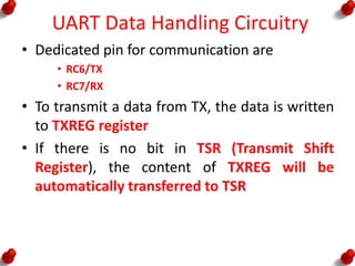
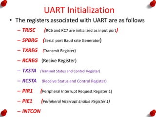
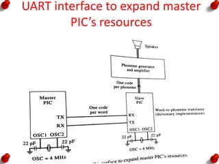
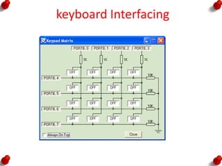
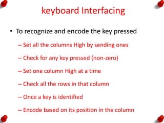
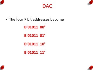
Unit III
Peripherals and Interfacing
T.Ramprakash
AP/ECE
Ramco Institute of Technology
Flow of Topics
• I2C Bus for Peripherals Chip Access
– I2C Bus operation
– I2C Bus subroutines
• Serial EEPROM
• Analog to Digital Converter
• UART
– Baud rate selection
– Data handling circuit
– Initialization
• LCD Interfacing
• Keyboard Interfacing
• Digital to Analog Converter
• Sensor Interfacing
I2C Bus for Peripherals Chip Access
• The name stands for “Inter - Integrated Circuit
Bus”
• A Small Area Network connecting ICs and
other electronic systems
• Developed by Philips Semiconductors
• I2C can support up to 128 slave Devices
• Today, a variety of devices are available with
I2C Interfaces
– Microcontroller, EEPROM, Real-Timer, interface
chips, LCD driver, A/D converter
I2C Bus for Peripherals Chip Access
Overview
• Used for moving data simply and quickly from
one device to another
• Serial Interface
• I2C is a synchronous protocol that allows a
master device to initiate communication with
a slave device.
• I2C is also bi-directional by which data is sent
either direction on the serial data line (SDA)
by the master or slave.
Overview
• I2C is a synchronous protocol which means,
– The data is clocked along with a clock signal (SCL)
– The clock signal controls when data is changed
and when it should be read
– Since I2C is synchronous, the clock rate can vary,
unlike asynchronous (RS-232 style)
communications
Overview
• I2C is a Master-Slave protocol that allows
– The Master device controls the clock (SCL)
– The slave devices may hold the clock low to
prevent data transfer
– No data is transferred unless a clock signal is
present
– All slaves are controlled by the master clock
I2C Bus operation
• It requires two open drain Input/output pins
• These two pins called SCL and SDA are implemented on
the PIC chips as two multipurpose pins
– RC3/SCK/SCL (Serial Clock)
– RC4/SDI/SDA (Serial Data)
open drain Input/output pins
Low output on
SCL or SDA
5V
1 K
High output on
SCL or SDA
I/O pin set to be an input
1 K
5V
Normal
Output
Driver
‘0’
PIC
I/O pin set to be an output
Overview
• SDA
– This signal is known as Serial Data.
– Any data sent from one device to another goes on
this line
• SCL
– This is the Serial Clock signal.
– It is generated by the master device and controls
when data is sent and when it is read.
Different Modes
• Standard mode (100 Kbits/sec)
• Full speed (400 Kbits/sec)
• Fast mode (1 Mbits/sec)
• High speed (3.2 Mbits/sec)
I2C Bus operation
• SDA line Transmits/Receives data bits (MSB is sent first)
• Data in SDA line is stable during clock (SCL) high
• Serial clock is driven by the master
• Acknowledgment bit is driven by the receiver after the
end of reception
• If the receiver does not acknowledge, SDA line remains
high
SDA
SCL
MSB
ACK driven by
receiverLSB
I2C Bus Communication
• The format of I2C bus transfers
Start Bit
• Initializes I2C Bus
• SDA is pulled low, then SCL is pulled low
Stop Bit
• Releases I2C Bus
• SCL is released first, then SDA is released
Control bits
• The start bit is followed 7 bit slave address
• Address bit is followed by R/W bit
• If R/W=0, subsequent bytes transmitted on the bus will
be written by the PIC to the selected peripheral
• If R/W=1, subsequent bytes will be sent by the selected
peripheral and read by the PIC
SDA
Slave Address
R/W
I2C typical message format
• For peripheral chip that contains more than one
internal register or memory address, the PIC will
typically write a second byte to the chip to set a pointer
to the selected internal register or the consecutive
addresses that follow it
I2C Bus subroutine
• SCL pin :must have an open drive output
• SDA pin: can be either input or have an open drive
output
• I2C bus subroutine will repeatedly access TRISC, the
data direction register for PORT C
bsf TRISC, 4 //SDA pin is in input mode
bcf TRISC, 4 //SDA pin is in output mode
• TRISC is located at Bank 1 address H’87’
bsf STATUS, RP0 //Selects Bank 1
bcf STATUS, RP0 //Selects Bank 0
I2C Bus subroutine
• Instead of this, load the indirect pointer FSR with the
address of TRISC
movlw TRISC
movwf FSR
• And then do the required bit setting and bit clearing of
TRISC bits indirectly
SCL equ 3
SDA equ 4
Then,
bsf INDF, SDA
I2C Bus subroutine transfers out three
bytes: DEVADD, INTADD and DATAOUT
main
call START
movf DEVADD, W //Send the device address with R/W=0
call TX
movf DATAOUT, W //Send data to the device
call TX
call STOP
return
Bit 7 : 0  No Collision
Bit 6 : 0  No Overflow
Bit 5 : 1  Enable SPI Mode
Bit 4 : 1  Enable SDA and SCL as source of serial port
START
movlw B’00111011’
movwf SSPCON
bcf PORTC, SDA
bcf PORTC, SCL
movlw TRISC
movwf FSR
TX
movwf TXBUFF
bsf STATUS, C
TX_1
rlf TXBUFF, F
movf TXBUFF, F
btfss STATUS,Z
call BitOut
btfss STATUS,Z
goto TX_1
call BitIn
movlw B’00000001’ //Check acknowledge bit
andwf RXBUFF, W // Z=1 if ACK, Z=0 of NOACK
return
BitOut
bcf INDF, SDA
btfsc STATUS, C //copy carry bit to SDA
bsf INDF, SDA
bsf INDF, SCL //Pulse clock line
delay 0,1,2
bcf INDF, SCL
bcf STATUS,C //clear carry bit
return
BitIn
bsf INDF, SDA
bsf INDF, SCL //Drive clock line and SDA line high
bcf RXBUFF,0
btfsc PORTC, SDA
bsf RXBUFF, 0
bcf INDF, SCL
return
STOP
bcf INDF, SDA //Return SDA LOW
bsf INDF, SCL //Drive SCL High
delay 0,1,2
bsf INDF, SDA //Drive SDA High
return
I2C Advantages
• It is faster than asynchronous serial communication
• Number of pins required for communication is less
(only 2 pins)
• I2C supports multi master system
• I2C supports up to 128 slave devices
• I2C supports slave acknowledgment
I2C Disadvantages
• Communication is more complex than UART or SPI
• I2C draws more power than other serial
communication
• Slower operational devices can slower the operations
of faster speed devices
• I2C bus can result in entire bus hanging
• I2C bus does not suits long range
EEPROM
EEPROM
• Nonvolatile Memory
• Microchip Technology – 24LC01B is an
EEPROM with I2C Serial Interaface
24LC01B EEPROM Characteristics
• 128 byte data
• Tiny eight pin DIP or surface mount package
• +5 V supply
• Fast Mode (400 kbits/sec) I2C bus.
• Draws less than 3mA during programming
• 1 mA during reading
• 0.1 mA during standby
24LC01B EEPROM Characteristics
• 8 Bytes at a time
• Programming time is less than 10 ms
• 10,000,000 erase/write cycles
• Data retention beyond 200 years
• 0o C to 70o
• -40o C to +85o C for industries
• WP (Write Protect) pin  manufacturer to program a part
Analog to Digital Converter
Introduction
• Analog to Digital Converter (ADC) is a device
that converts an analog quantity (continuous
voltage) to discrete digital values
• The analog input voltage must be within the
valid input range of the A/D for an accurate
conversion
ADC Features
• Five to Eight Input channels
• 8 bit conversion
• An Analog Multiplexer
• Sample and Hold circuit
• Adjustable sampling rate
• Internal or External reference voltage
• Interrupt to controller at the end of conversion
ADC Characteristics
• It converts an input voltage to an 8 bit number
• Input voltage is scaled against a reference voltage VREF
• The reference voltage used for many application is the
PIC supply voltage, VDD (VREF = VDD)
• ADC operation requires
0V <= VINPUT <= VREF
3 V <= VREF <= VDD
ADC Characteristics
• Resolution defines the number of possible
output states (2n states - n is the number of
bits of the converter)
• 8-bit converter has 28=256 states
• Higher resolution = less quantization error
ADC Characteristics
1/256 2/256 256/256…………………….
Digital
Output
Input voltage / VRef
H’00’
H’01’
H’02’
H’FF’
ADC inputs with VREF = VDD
P
O
R
T
A
P
O
R
T
E
0
1
2
3
4
5
0
2
1
Analog Input or
Digital I/O
Analog Input only
Digital I/O only
ADC Module
Acquisition time
• Acquisition time is the time required to charge
and discharge the holding capacitor on the
front end of an ADC
• If sufficient time is not allowed for acquisition
the conversion result will be inaccurate
ADCON0 Register
2
000 Select Analog Input on PORTA, bit 0
001 Select Analog Input on PORTA, bit 1
010 Select Analog Input on PORTA, bit 2
011 Select Analog Input on PORTA, bit 3
100 Select Analog Input on PORTA, bit 5
101 Select Analog Input on PORTE, bit 0
110 Select Analog Input on PORTE, bit 1
111 Select Analog Input on PORTE, bit 2
Conversion Time
• 15 Microseconds for OSC=20MHz
• 30 Microseconds for OSC=10MHz
UART
Overview
Communication
Serial Communication Parallel Communication
Overview
Serial Communication Parallel Communication
Overview
Communication
Synchronous Communication Asynchronous Communication
Synchronous Communication
• The information is transmitted from the
transmitter in sequence, bit after bit, with
fixed baud rate, when the clock frequency
along with the bits are transmitted to the
receiver.
• This means that the transmitter and the
receiver are synchronized between them by
the same clock frequency.
Asynchronous Communication
• In this case, the information is divided into
frames, in the size of byte.
• Each one of the frame has a “Start” bit and a
“Stop” bit.
• “Start” bit marks the beginning of a new
frame, “Stop” bit marks the end.
• Frames of information must not necessarily
be transmitted at equal time space, since
they are independent of the clock.
UART Overview
• UART  Universal Asynchronous Receiver
Transmitter
• The PICs including UART module are
– PIC 16C63
– PIC 16C65A
– PIC 16C73
– PIC 16C73A
Waveforms and Baud-Rate Accuracy
• When serial data is transmitted
asynchronously, the data stream is generated
with the transmitter’s clock
• The receiver must synchronize the incoming
data stream to the receiver’s clock
Waveforms and Baud-Rate Accuracy
• Each 8 bit data is framed by a START bit and
STOP bit
• For transmission at 9,600 Bd, each of these
bits lasts for a bit time (BT) of 1/9,600
seconds
Baud-Rate Selection
• To set desirable baud rate, it is necessary to
determine a new value of a clock system.
• The value of the clock will be determined by
the hexadecimal number inserted into register
SPBRG (Serial Port Baud Rate Generator Register)
• The PIC can transmit at a
high rate: BRGH=1
low rate: BRGH=0.
Baud-Rate Selection
• The calculation of the hexadecimal number
inserted into register SPBRG done using the
following formulas
Baud-Rate Selection
• (Ex) Calculate the hexadecimal value to be
insert into the register SPBRG, to get a
transmission baud rate of 1200 bps at a lower
rate.
UART Data Handling Circuitry
• Dedicated pin for communication are
• RC6/TX
• RC7/RX
• To transmit a data from TX, the data is written
to TXREG register
• If there is no bit in TSR (Transmit Shift
Register), the content of TXREG will be
automatically transferred to TSR
Transmit Data Circuit
UART Data Handling Circuitry
• The received data is shifted to RSR (Receive Data
Circuit)
• Here, the STOP bit is checked and an error flag is
set if the STOP bit does not equal to one
• The received byte is automatically transferred to
2-Byte FIFO
• If FIFO is empty, the received byte will fall
through RCREG
• If FIFO is full, and if third byte enters the RX pin,
then the third byte will be lost
• An overflow error flag will be set, alerting the
receiver software of the loss of a byte of data
Receive Data Circuit
UART Initialization
• The registers associated with UART are as follows
– TRISC (RC6 and RC7 are initialized as input port)
– SPBRG (Serial port Baud rate Generator)
– TXREG (Transmit Register)
– RCREG (Recive Register)
– TXSTA (Transmit Status and Control Register)
– RCSTA (Receive Status and Control Register)
– PIR1 (Peripheral Interrupt Request Register 1)
– PIE1 (Peripheral Interrupt Enable Register 1)
– INTCON
UART Initialization
1 1 X X X X X X
RC7/RX RC6/TX
01234567
TRIS C
SPBRG
Serial port Baud rate Generator
TXREG
RCREG
Transmit Register
Receive Register
UART Initialization
TXSTA
RCSTA
1: High speed baud rate
0: Low speed baud rate
1: Enable Transmit Function
0: Disable Transmit Function
1: Overrun Error has occurred
0: No overrun error
1: Framing Error has occurred
0: No framing error
1: Enable Receive function
0: Disable Receive function
1: Serial port Enabled
0: Serial Port Disabled
UART Initialization
PIR1
1: when TXREG is empty and ready for next transmission
0: when TXREG is full
1: when byte is available in RCREG
0: when FIFO is cleared
PIE1
1: Enable interrupt when TSIF =1
0: Disable interrupt when TSIF =1
1: Enable interrupt when RCIF =1
0: Disable interrupt when RCIF =1
UART Initialization
INTCON
Peripheral Interrupt Enable BitGlobal Interrupt Enable Bit
UART USE
• The major application of PIC’s UART is to
provide two wire serial interface to personal
computer
• Both PIC and PC should be setup for the same
baud rate
• One Start Bit, 8 Data Bit and One Stop Bit
UART USE
UART USE
UART interconnection of two PICs
• Another application of the PIC UART is to
couple two PIC’s together
• By this, some of the work can be off loaded to
other PIC
UART interconnection of two PICs
OSC = 4MHz OSC = 10 MHz OSC=20 MHz
Baud Rate 250 Kbaud 625 Kbaud 1.25 Mbaud
Time to
transfer one
byte
40 uSec 16 uSec 8 uSec
UART interface to expand master
PIC’s resources
LCD and keyboard Interfacing
Keyboard Interfacing
• Keypad interfacing must have two process
– Key press Detection
– Key identification
• Two ways to identify the key press
– Interrupt Method
– Scanning Method
Keyboard Interfacing
• Key Bouncing
• Mechanical switches are used as keys in most of the
keyboards.
• When a key is pressed the contact bounce back and
forth and settle down only after a small time delay
(about 20ms).
• Even though a key is actuated once, it will appear to
have been actuated several times.
• This problem is called Key Bouncing.
keyboard Interfacing
• 4 x 4 matrix keypad organized in the row and column
format
• Four columns are connected to the lower half of
PORTB (RB0-RB3)
• Four rows are connected to upper half of PORTB
(RB4-RB7)
• When a key is pressed, it makes a contact with the
corresponding row and column
keyboard Interfacing
• To recognize and encode the key pressed
– Set all the columns High by sending ones
– Check for any key pressed (non-zero)
– Set one column High at a time
– Check all the rows in that column
– Once a key is identified
– Encode based on its position in the column
DAC
DAC
• Two digital to analog converters are easily
added to PIC with MAX 518.
• MAX518 is a eight pin DIP or SO-8 surface
mount
• Each output channel produces an output
voltage that ranges from
0 V to 255/256ths of power supply
DAC
DAC
• The MAX5128 chip includes a power on reset
circuit that drives the two outputs to 0V
initially
• The two address inputs AD1 and AD0 provide
an adjustable part of the chip’s I2C address
• With a help of Five bits (01011) and two
adjustable bits, we can connect four MAX518
chips to a PIC
DAC
DAC
• The four 7 bit addresses become
B’01011 00’
B’01011 01’
B’01011 10’
B’01011 11’
DAC
0 1 0 1 1 AD0 AD1 0
0 0 0 0 0 0 0 0
Write
0 - OUT0
1 - OUT1
0 - Normal DAC operation
1 - Reset all DAC Register
0 - Normal DAC operation
1 - Power Down mode
DAC
Analog Output Voltage = VDD *B/256
• An output of 2.5 V will appear on the OUT0
pin if the following three bytes are sent to the
chip
B’01011000’ B’00000000’ B’10000000’
• An output of 1.25 V will appear on the OUT1
pin if the following three bytes are sent to the
chip
B’01011000’ B’00000001’ B’01000000’
Sensor Interfacing
Sensor Interfacing
• Transducer convert physical data such as
temperature , light intensity, flow and speed
to electrical signals
• Depending on the transducer the output
produced is in the form of voltage or current
or resistance or capacitance
Temperature Sensor (LM 75)
• National Semiconductors LM75 chip converts
temperatures over the range of
• -25oC to +100oC with +- 2oC accuracy
• -55oC up to +125oC with +- 3oC accuracy
• 0.5oC resolution
• 9bit ADC
Temperature Sensor (LM 75)
Temperature Digital Output
Binary Decimal
+125oC 0 1111 1010 250
+25oC 0 0011 0010 50
+0.5oC 0 0000 0001 1
0oC 0 0000 0000 2
-0.5oC 1 1111 1111 512-1=511
-25oC 1 1100 1110 512-50=462
-55oC 1 1001 0010 512-110=402
Temperature Sensor (LM 75)
• LM75 chip includes thermal watchdog that
can be set up to interrupt the PIC on its
RB0/INT edge triggered interrupt input when
the temperature rises past a programmable
set point (Tos (overtemperature shutdown ) )
• It includes programmable hysteresis (THYST) so
that the temperature must dip down below
the set point T
Temperature Sensor (LM 75)
Reference
1. Peatman,J.B., “Design with PIC Micro
Controllers”PearsonEducation,3rdEdition,
2004.
2. Furber,S., “ARM System on Chip Architecture”
Addison Wesley trade Computer
Publication, 2000

Peripherals and interfacing

  • 1.
    Unit III Peripherals andInterfacing T.Ramprakash AP/ECE Ramco Institute of Technology
  • 2.
    Flow of Topics •I2C Bus for Peripherals Chip Access – I2C Bus operation – I2C Bus subroutines • Serial EEPROM • Analog to Digital Converter • UART – Baud rate selection – Data handling circuit – Initialization • LCD Interfacing • Keyboard Interfacing • Digital to Analog Converter • Sensor Interfacing
  • 3.
    I2C Bus forPeripherals Chip Access • The name stands for “Inter - Integrated Circuit Bus” • A Small Area Network connecting ICs and other electronic systems • Developed by Philips Semiconductors • I2C can support up to 128 slave Devices • Today, a variety of devices are available with I2C Interfaces – Microcontroller, EEPROM, Real-Timer, interface chips, LCD driver, A/D converter
  • 4.
    I2C Bus forPeripherals Chip Access
  • 5.
    Overview • Used formoving data simply and quickly from one device to another • Serial Interface • I2C is a synchronous protocol that allows a master device to initiate communication with a slave device. • I2C is also bi-directional by which data is sent either direction on the serial data line (SDA) by the master or slave.
  • 6.
    Overview • I2C isa synchronous protocol which means, – The data is clocked along with a clock signal (SCL) – The clock signal controls when data is changed and when it should be read – Since I2C is synchronous, the clock rate can vary, unlike asynchronous (RS-232 style) communications
  • 7.
    Overview • I2C isa Master-Slave protocol that allows – The Master device controls the clock (SCL) – The slave devices may hold the clock low to prevent data transfer – No data is transferred unless a clock signal is present – All slaves are controlled by the master clock
  • 8.
    I2C Bus operation •It requires two open drain Input/output pins • These two pins called SCL and SDA are implemented on the PIC chips as two multipurpose pins – RC3/SCK/SCL (Serial Clock) – RC4/SDI/SDA (Serial Data)
  • 9.
    open drain Input/outputpins Low output on SCL or SDA 5V 1 K High output on SCL or SDA I/O pin set to be an input 1 K 5V Normal Output Driver ‘0’ PIC I/O pin set to be an output
  • 10.
    Overview • SDA – Thissignal is known as Serial Data. – Any data sent from one device to another goes on this line • SCL – This is the Serial Clock signal. – It is generated by the master device and controls when data is sent and when it is read.
  • 11.
    Different Modes • Standardmode (100 Kbits/sec) • Full speed (400 Kbits/sec) • Fast mode (1 Mbits/sec) • High speed (3.2 Mbits/sec)
  • 12.
    I2C Bus operation •SDA line Transmits/Receives data bits (MSB is sent first) • Data in SDA line is stable during clock (SCL) high • Serial clock is driven by the master • Acknowledgment bit is driven by the receiver after the end of reception • If the receiver does not acknowledge, SDA line remains high SDA SCL MSB ACK driven by receiverLSB
  • 13.
    I2C Bus Communication •The format of I2C bus transfers
  • 14.
    Start Bit • InitializesI2C Bus • SDA is pulled low, then SCL is pulled low
  • 15.
    Stop Bit • ReleasesI2C Bus • SCL is released first, then SDA is released
  • 16.
    Control bits • Thestart bit is followed 7 bit slave address • Address bit is followed by R/W bit • If R/W=0, subsequent bytes transmitted on the bus will be written by the PIC to the selected peripheral • If R/W=1, subsequent bytes will be sent by the selected peripheral and read by the PIC SDA Slave Address R/W
  • 17.
  • 18.
    I2C typical messageformat • For peripheral chip that contains more than one internal register or memory address, the PIC will typically write a second byte to the chip to set a pointer to the selected internal register or the consecutive addresses that follow it
  • 19.
    I2C Bus subroutine •SCL pin :must have an open drive output • SDA pin: can be either input or have an open drive output • I2C bus subroutine will repeatedly access TRISC, the data direction register for PORT C bsf TRISC, 4 //SDA pin is in input mode bcf TRISC, 4 //SDA pin is in output mode • TRISC is located at Bank 1 address H’87’ bsf STATUS, RP0 //Selects Bank 1 bcf STATUS, RP0 //Selects Bank 0
  • 20.
    I2C Bus subroutine •Instead of this, load the indirect pointer FSR with the address of TRISC movlw TRISC movwf FSR • And then do the required bit setting and bit clearing of TRISC bits indirectly SCL equ 3 SDA equ 4 Then, bsf INDF, SDA
  • 21.
    I2C Bus subroutinetransfers out three bytes: DEVADD, INTADD and DATAOUT main call START movf DEVADD, W //Send the device address with R/W=0 call TX movf DATAOUT, W //Send data to the device call TX call STOP return
  • 22.
    Bit 7 :0  No Collision Bit 6 : 0  No Overflow Bit 5 : 1  Enable SPI Mode Bit 4 : 1  Enable SDA and SCL as source of serial port
  • 23.
    START movlw B’00111011’ movwf SSPCON bcfPORTC, SDA bcf PORTC, SCL movlw TRISC movwf FSR
  • 24.
    TX movwf TXBUFF bsf STATUS,C TX_1 rlf TXBUFF, F movf TXBUFF, F btfss STATUS,Z call BitOut btfss STATUS,Z goto TX_1 call BitIn movlw B’00000001’ //Check acknowledge bit andwf RXBUFF, W // Z=1 if ACK, Z=0 of NOACK return
  • 25.
    BitOut bcf INDF, SDA btfscSTATUS, C //copy carry bit to SDA bsf INDF, SDA bsf INDF, SCL //Pulse clock line delay 0,1,2 bcf INDF, SCL bcf STATUS,C //clear carry bit return
  • 26.
    BitIn bsf INDF, SDA bsfINDF, SCL //Drive clock line and SDA line high bcf RXBUFF,0 btfsc PORTC, SDA bsf RXBUFF, 0 bcf INDF, SCL return
  • 27.
    STOP bcf INDF, SDA//Return SDA LOW bsf INDF, SCL //Drive SCL High delay 0,1,2 bsf INDF, SDA //Drive SDA High return
  • 28.
    I2C Advantages • Itis faster than asynchronous serial communication • Number of pins required for communication is less (only 2 pins) • I2C supports multi master system • I2C supports up to 128 slave devices • I2C supports slave acknowledgment
  • 29.
    I2C Disadvantages • Communicationis more complex than UART or SPI • I2C draws more power than other serial communication • Slower operational devices can slower the operations of faster speed devices • I2C bus can result in entire bus hanging • I2C bus does not suits long range
  • 30.
  • 31.
    EEPROM • Nonvolatile Memory •Microchip Technology – 24LC01B is an EEPROM with I2C Serial Interaface
  • 32.
    24LC01B EEPROM Characteristics •128 byte data • Tiny eight pin DIP or surface mount package • +5 V supply • Fast Mode (400 kbits/sec) I2C bus. • Draws less than 3mA during programming • 1 mA during reading • 0.1 mA during standby
  • 33.
    24LC01B EEPROM Characteristics •8 Bytes at a time • Programming time is less than 10 ms • 10,000,000 erase/write cycles • Data retention beyond 200 years • 0o C to 70o • -40o C to +85o C for industries • WP (Write Protect) pin  manufacturer to program a part
  • 34.
  • 35.
    Introduction • Analog toDigital Converter (ADC) is a device that converts an analog quantity (continuous voltage) to discrete digital values • The analog input voltage must be within the valid input range of the A/D for an accurate conversion
  • 36.
    ADC Features • Fiveto Eight Input channels • 8 bit conversion • An Analog Multiplexer • Sample and Hold circuit • Adjustable sampling rate • Internal or External reference voltage • Interrupt to controller at the end of conversion
  • 37.
    ADC Characteristics • Itconverts an input voltage to an 8 bit number • Input voltage is scaled against a reference voltage VREF • The reference voltage used for many application is the PIC supply voltage, VDD (VREF = VDD) • ADC operation requires 0V <= VINPUT <= VREF 3 V <= VREF <= VDD
  • 38.
    ADC Characteristics • Resolutiondefines the number of possible output states (2n states - n is the number of bits of the converter) • 8-bit converter has 28=256 states • Higher resolution = less quantization error
  • 39.
    ADC Characteristics 1/256 2/256256/256……………………. Digital Output Input voltage / VRef H’00’ H’01’ H’02’ H’FF’
  • 40.
    ADC inputs withVREF = VDD P O R T A P O R T E 0 1 2 3 4 5 0 2 1 Analog Input or Digital I/O Analog Input only Digital I/O only
  • 41.
  • 42.
    Acquisition time • Acquisitiontime is the time required to charge and discharge the holding capacitor on the front end of an ADC • If sufficient time is not allowed for acquisition the conversion result will be inaccurate
  • 43.
    ADCON0 Register 2 000 SelectAnalog Input on PORTA, bit 0 001 Select Analog Input on PORTA, bit 1 010 Select Analog Input on PORTA, bit 2 011 Select Analog Input on PORTA, bit 3 100 Select Analog Input on PORTA, bit 5 101 Select Analog Input on PORTE, bit 0 110 Select Analog Input on PORTE, bit 1 111 Select Analog Input on PORTE, bit 2
  • 44.
    Conversion Time • 15Microseconds for OSC=20MHz • 30 Microseconds for OSC=10MHz
  • 45.
  • 46.
  • 47.
  • 48.
  • 49.
    Synchronous Communication • Theinformation is transmitted from the transmitter in sequence, bit after bit, with fixed baud rate, when the clock frequency along with the bits are transmitted to the receiver. • This means that the transmitter and the receiver are synchronized between them by the same clock frequency.
  • 50.
    Asynchronous Communication • Inthis case, the information is divided into frames, in the size of byte. • Each one of the frame has a “Start” bit and a “Stop” bit. • “Start” bit marks the beginning of a new frame, “Stop” bit marks the end. • Frames of information must not necessarily be transmitted at equal time space, since they are independent of the clock.
  • 51.
    UART Overview • UART Universal Asynchronous Receiver Transmitter • The PICs including UART module are – PIC 16C63 – PIC 16C65A – PIC 16C73 – PIC 16C73A
  • 52.
    Waveforms and Baud-RateAccuracy • When serial data is transmitted asynchronously, the data stream is generated with the transmitter’s clock • The receiver must synchronize the incoming data stream to the receiver’s clock
  • 53.
    Waveforms and Baud-RateAccuracy • Each 8 bit data is framed by a START bit and STOP bit • For transmission at 9,600 Bd, each of these bits lasts for a bit time (BT) of 1/9,600 seconds
  • 54.
    Baud-Rate Selection • Toset desirable baud rate, it is necessary to determine a new value of a clock system. • The value of the clock will be determined by the hexadecimal number inserted into register SPBRG (Serial Port Baud Rate Generator Register) • The PIC can transmit at a high rate: BRGH=1 low rate: BRGH=0.
  • 55.
    Baud-Rate Selection • Thecalculation of the hexadecimal number inserted into register SPBRG done using the following formulas
  • 56.
    Baud-Rate Selection • (Ex)Calculate the hexadecimal value to be insert into the register SPBRG, to get a transmission baud rate of 1200 bps at a lower rate.
  • 57.
    UART Data HandlingCircuitry • Dedicated pin for communication are • RC6/TX • RC7/RX • To transmit a data from TX, the data is written to TXREG register • If there is no bit in TSR (Transmit Shift Register), the content of TXREG will be automatically transferred to TSR
  • 58.
  • 59.
    UART Data HandlingCircuitry • The received data is shifted to RSR (Receive Data Circuit) • Here, the STOP bit is checked and an error flag is set if the STOP bit does not equal to one • The received byte is automatically transferred to 2-Byte FIFO • If FIFO is empty, the received byte will fall through RCREG • If FIFO is full, and if third byte enters the RX pin, then the third byte will be lost • An overflow error flag will be set, alerting the receiver software of the loss of a byte of data
  • 60.
  • 61.
    UART Initialization • Theregisters associated with UART are as follows – TRISC (RC6 and RC7 are initialized as input port) – SPBRG (Serial port Baud rate Generator) – TXREG (Transmit Register) – RCREG (Recive Register) – TXSTA (Transmit Status and Control Register) – RCSTA (Receive Status and Control Register) – PIR1 (Peripheral Interrupt Request Register 1) – PIE1 (Peripheral Interrupt Enable Register 1) – INTCON
  • 62.
    UART Initialization 1 1X X X X X X RC7/RX RC6/TX 01234567 TRIS C SPBRG Serial port Baud rate Generator TXREG RCREG Transmit Register Receive Register
  • 63.
    UART Initialization TXSTA RCSTA 1: Highspeed baud rate 0: Low speed baud rate 1: Enable Transmit Function 0: Disable Transmit Function 1: Overrun Error has occurred 0: No overrun error 1: Framing Error has occurred 0: No framing error 1: Enable Receive function 0: Disable Receive function 1: Serial port Enabled 0: Serial Port Disabled
  • 64.
    UART Initialization PIR1 1: whenTXREG is empty and ready for next transmission 0: when TXREG is full 1: when byte is available in RCREG 0: when FIFO is cleared PIE1 1: Enable interrupt when TSIF =1 0: Disable interrupt when TSIF =1 1: Enable interrupt when RCIF =1 0: Disable interrupt when RCIF =1
  • 65.
    UART Initialization INTCON Peripheral InterruptEnable BitGlobal Interrupt Enable Bit
  • 66.
    UART USE • Themajor application of PIC’s UART is to provide two wire serial interface to personal computer • Both PIC and PC should be setup for the same baud rate • One Start Bit, 8 Data Bit and One Stop Bit
  • 67.
  • 68.
  • 69.
    UART interconnection oftwo PICs • Another application of the PIC UART is to couple two PIC’s together • By this, some of the work can be off loaded to other PIC
  • 70.
    UART interconnection oftwo PICs OSC = 4MHz OSC = 10 MHz OSC=20 MHz Baud Rate 250 Kbaud 625 Kbaud 1.25 Mbaud Time to transfer one byte 40 uSec 16 uSec 8 uSec
  • 71.
    UART interface toexpand master PIC’s resources
  • 72.
    LCD and keyboardInterfacing
  • 73.
    LCD and keyboardInterfacing
  • 74.
    Keyboard Interfacing • Keypadinterfacing must have two process – Key press Detection – Key identification • Two ways to identify the key press – Interrupt Method – Scanning Method
  • 75.
    Keyboard Interfacing • KeyBouncing • Mechanical switches are used as keys in most of the keyboards. • When a key is pressed the contact bounce back and forth and settle down only after a small time delay (about 20ms). • Even though a key is actuated once, it will appear to have been actuated several times. • This problem is called Key Bouncing.
  • 76.
    keyboard Interfacing • 4x 4 matrix keypad organized in the row and column format • Four columns are connected to the lower half of PORTB (RB0-RB3) • Four rows are connected to upper half of PORTB (RB4-RB7) • When a key is pressed, it makes a contact with the corresponding row and column
  • 77.
  • 78.
    keyboard Interfacing • Torecognize and encode the key pressed – Set all the columns High by sending ones – Check for any key pressed (non-zero) – Set one column High at a time – Check all the rows in that column – Once a key is identified – Encode based on its position in the column
  • 79.
  • 80.
    DAC • Two digitalto analog converters are easily added to PIC with MAX 518. • MAX518 is a eight pin DIP or SO-8 surface mount • Each output channel produces an output voltage that ranges from 0 V to 255/256ths of power supply
  • 81.
  • 82.
    DAC • The MAX5128chip includes a power on reset circuit that drives the two outputs to 0V initially • The two address inputs AD1 and AD0 provide an adjustable part of the chip’s I2C address • With a help of Five bits (01011) and two adjustable bits, we can connect four MAX518 chips to a PIC
  • 83.
  • 84.
    DAC • The four7 bit addresses become B’01011 00’ B’01011 01’ B’01011 10’ B’01011 11’
  • 85.
    DAC 0 1 01 1 AD0 AD1 0 0 0 0 0 0 0 0 0 Write 0 - OUT0 1 - OUT1 0 - Normal DAC operation 1 - Reset all DAC Register 0 - Normal DAC operation 1 - Power Down mode
  • 86.
    DAC Analog Output Voltage= VDD *B/256 • An output of 2.5 V will appear on the OUT0 pin if the following three bytes are sent to the chip B’01011000’ B’00000000’ B’10000000’ • An output of 1.25 V will appear on the OUT1 pin if the following three bytes are sent to the chip B’01011000’ B’00000001’ B’01000000’
  • 87.
  • 88.
    Sensor Interfacing • Transducerconvert physical data such as temperature , light intensity, flow and speed to electrical signals • Depending on the transducer the output produced is in the form of voltage or current or resistance or capacitance
  • 89.
    Temperature Sensor (LM75) • National Semiconductors LM75 chip converts temperatures over the range of • -25oC to +100oC with +- 2oC accuracy • -55oC up to +125oC with +- 3oC accuracy • 0.5oC resolution • 9bit ADC
  • 90.
  • 91.
    Temperature Sensor (LM75) Temperature Digital Output Binary Decimal +125oC 0 1111 1010 250 +25oC 0 0011 0010 50 +0.5oC 0 0000 0001 1 0oC 0 0000 0000 2 -0.5oC 1 1111 1111 512-1=511 -25oC 1 1100 1110 512-50=462 -55oC 1 1001 0010 512-110=402
  • 92.
    Temperature Sensor (LM75) • LM75 chip includes thermal watchdog that can be set up to interrupt the PIC on its RB0/INT edge triggered interrupt input when the temperature rises past a programmable set point (Tos (overtemperature shutdown ) ) • It includes programmable hysteresis (THYST) so that the temperature must dip down below the set point T
  • 93.
  • 94.
  • 95.
  • 96.
  • 97.
  • 98.
    Reference 1. Peatman,J.B., “Designwith PIC Micro Controllers”PearsonEducation,3rdEdition, 2004. 2. Furber,S., “ARM System on Chip Architecture” Addison Wesley trade Computer Publication, 2000