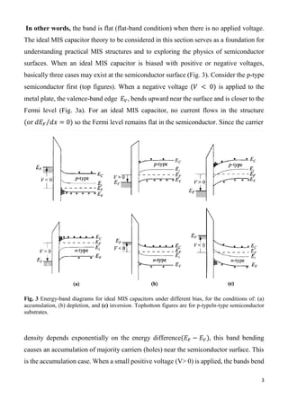
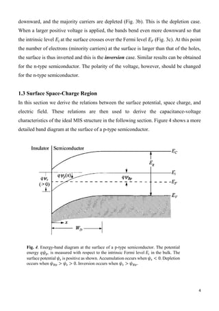
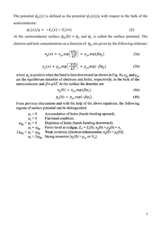
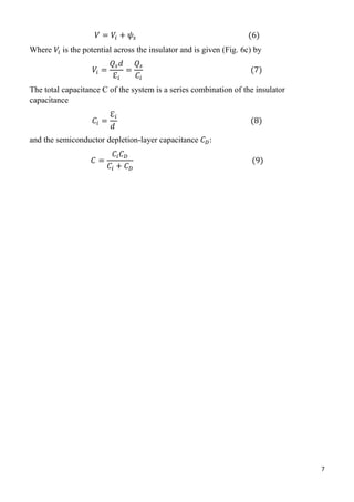
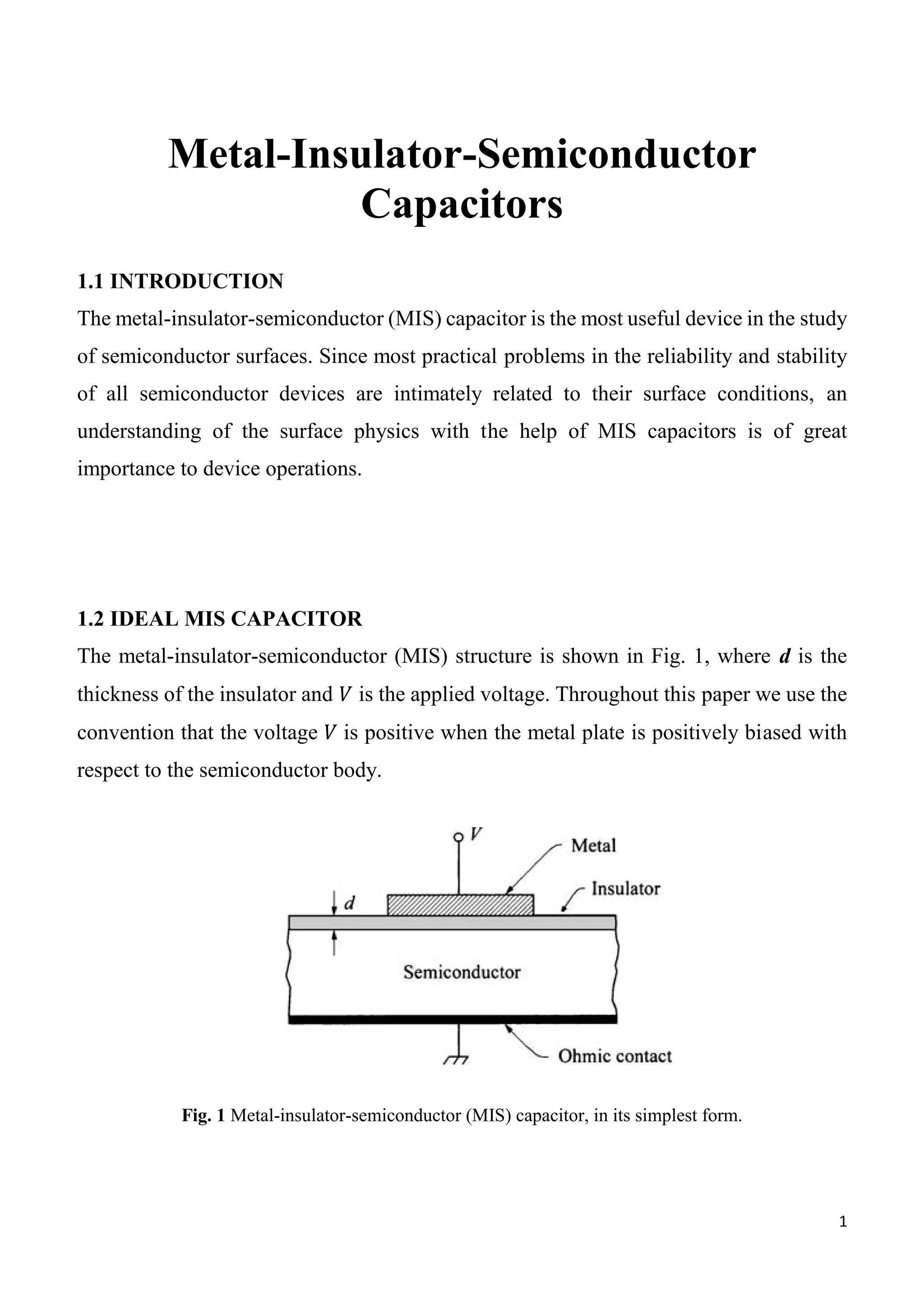
1
Metal-Insulator-Semiconductor
Capacitors
1.1 INTRODUCTION
The metal-insulator-semiconductor (MIS) capacitor is the most useful device in the study
of semiconductor surfaces. Since most practical problems in the reliability and stability
of all semiconductor devices are intimately related to their surface conditions, an
understanding of the surface physics with the help of MIS capacitors is of great
importance to device operations.
1.2 IDEAL MIS CAPACITOR
The metal-insulator-semiconductor (MIS) structure is shown in Fig. 1, where d is the
thickness of the insulator and 𝑉 is the applied voltage. Throughout this paper we use the
convention that the voltage 𝑉 is positive when the metal plate is positively biased with
respect to the semiconductor body.
Fig. 1 Metal-insulator-semiconductor (MIS) capacitor, in its simplest form.
2
Fig. 2, for both n-type and p-type semiconductors. An ideal MIS capacitor is defined as
follows: (1) The only charges that can exist in the structure under any biasing conditions
are those in the semiconductor and those, with an equal but opposite sign, on the metal
surface adjacent to the insulator, i.e., there is no interface trap nor any kind of oxide
charge; (2) There is no carrier transport through the insulator under dc biasing
conditions or the resistivity of the insulator is infinite. Furthermore.
Fig. 2 Energy-band diagrams of ideal MIS capacitors at equilibrium (V= 0). (a) n-type semiconductor.
(b) p-type semiconductor.
For the sake of simplicity we assume the metal is chosen such that the difference between
the metal work function ∅ 𝑚 and the semiconductor work function is zero, or ∅ 𝒎𝒔 = 0.
The above conditions, with the help of Fig. 2, are equivalent to:
∅ 𝑚𝑠 = ∅ 𝑚 − [𝑥 +
𝐸𝑔
2𝑞
− 𝜑 𝐵𝑛] = ∅ 𝑚 − (𝑥 + ∅ 𝑛) = 0 𝑓𝑜𝑟 𝑛 − 𝑡𝑦𝑝𝑒 (1𝑎)
∅ 𝑚𝑠 = ∅ 𝑚 − [𝑥 +
𝐸𝑔
2𝑞
− 𝜑 𝐵𝑝] = ∅ 𝑚 − (𝑥 +
𝐸𝑔
𝑞
− ∅ 𝑝) = 0 𝑓𝑜𝑟 𝑝 − 𝑡𝑦𝑝𝑒 (1𝑏)
Where 𝑥 and 𝑥𝑖 are the electron affinities for the semiconductor and insulator
respectively, and 𝜑 𝐵𝑝, 𝜑 𝐵𝑛, ∅ 𝑛, ∅ 𝑝 are the Fermi potentials with respect to the mid gap
and band edges.
3
In other words, the band is flat (flat-band condition) when there is no applied voltage.
The ideal MIS capacitor theory to be considered in this section serves as a foundation for
understanding practical MIS structures and to exploring the physics of semiconductor
surfaces. When an ideal MIS capacitor is biased with positive or negative voltages,
basically three cases may exist at the semiconductor surface (Fig. 3). Consider the p-type
semiconductor first (top figures). When a negative voltage (𝑉 < 0) is applied to the
metal plate, the valence-band edge 𝐸 𝑉, bends upward near the surface and is closer to the
Fermi level (Fig. 3a). For an ideal MIS capacitor, no current flows in the structure
(or 𝑑𝐸 𝐹 𝑑𝑥⁄ = 0) so the Fermi level remains flat in the semiconductor. Since the carrier
Fig. 3 Energy-band diagrams for ideal MIS capacitors under different bias, for the conditions of: (a)
accumulation, (b) depletion, and (c) inversion. Tophottom figures are for p-typeln-type semiconductor
substrates.
density depends exponentially on the energy difference(𝐸 𝐹 − 𝐸 𝑉), this band bending
causes an accumulation of majority carriers (holes) near the semiconductor surface. This
is the accumulation case. When a small positive voltage (V> 0) is applied, the bands bend
4
downward, and the majority carriers are depleted (Fig. 3b). This is the depletion case.
When a larger positive voltage is applied, the bands bend even more downward so that
the intrinsic level 𝐸𝑖 at the surface crosses over the Fermi level 𝐸 𝐹 (Fig. 3c). At this point
the number of electrons (minority carriers) at the surface is larger than that of the holes,
the surface is thus inverted and this is the inversion case. Similar results can be obtained
for the n-type semiconductor. The polarity of the voltage, however, should be changed
for the n-type semiconductor.
1.3 Surface Space-Charge Region
In this section we derive the relations between the surface potential, space charge, and
electric field. These relations are then used to derive the capacitance-voltage
characteristics of the ideal MIS structure in the following section. Figure 4 shows a more
detailed band diagram at the surface of a p-type semiconductor.
Fig. 4. Energy-band diagram at the surface of a p-type semiconductor. The potential
energy 𝑞𝜓 𝑝, is measured with respect to the intrinsic Fermi level 𝐸𝑖 in the bulk. The
surface potential 𝜓𝑠 is positive as shown. Accumulation occurs when 𝜓𝑠 < 0. Depletion
occurs when 𝜓 𝐵𝑝 > 𝜓𝑠 > 0. Inversion occurs when 𝜓𝑠 > 𝜓 𝐵𝑝.
5
The potential 𝜓 𝑝(𝑥) is defined as the potential 𝜓𝑖(𝑥)/𝑞 with respect to the bulk of the
semiconductor:
𝜓𝑖(𝑥) 𝑞⁄ = −𝐸𝑖(𝑥) − 𝐸𝑖(∞) (2)
At the semiconductor surface, 𝜓 𝑝(0) = 𝜓𝑠 and 𝜓𝑠 is called the surface potential. The
electron and hole concentrations as a function of 𝜓 𝑝 are given by the following relations:
6
Fig. 5 Variation of space-charge density in the semiconductor as a function of the surface potential
𝜓𝑠, for a p-type silicon with 𝑁𝐴 = 4 × 10¹⁵
at room temperature.
1.4 Ideal MIS Capacitance Curves
Figure 6a shows the band diagram of an ideal MIS structure with the band bending of
the semiconductor similar to that shown in Fig. 4 but in strong inversion. The charge
distribution is shown in Fig. 6b. For charge neutrality of the system, it is required that
𝑄 𝑚 = −(𝑄 𝑛 + 𝑞𝑁𝐴 𝑊𝐷) = −𝑄𝑠 (5)
where 𝑄 𝑚 is charges per unit area on the metal, 𝑄 𝑛, is the electrons per unit area near the
surface of the inversion region, 𝑞𝑁𝐴 𝑊𝐷 is the ionized acceptors per unit area in the space-
charge region with depletion width 𝑊𝐷 and 𝑄𝑠, is the total charges per unit area in the
semiconductor. The electric field and the potential as obtained by first and second
integrations of the Poisson equation are shown in Figs. 6c and d, respectively.
Clearly, in the absence of any work-function difference, the applied voltage will partly
appear across the insulator and partly across the semiconductor. Thus
7
𝑉 = 𝑉𝑖 + 𝜓𝑠 (6)
Where 𝑉𝑖 is the potential across the insulator and is given (Fig. 6c) by
𝑉𝑖 =
𝑄𝑠 𝑑
ℇ𝑖
=
𝑄𝑠
𝐶𝑖
(7)
The total capacitance C of the system is a series combination of the insulator
capacitance
𝐶𝑖 =
ℇ𝑖
𝑑
(8)
and the semiconductor depletion-layer capacitance 𝐶 𝐷:
𝐶 =
𝐶𝑖 𝐶 𝐷
𝐶𝑖 + 𝐶 𝐷
(9)
8
Fig. 6 (a) Band diagram of an ideal MIS capacitor under strong inversion. (b) Charge distribution.
(c) Electric-field distribution. (d) Potential distribution (relative to the semiconductor bulk)
9
For a given insulator thickness d, the value of Ci, is constant and corresponds to the
maximum capacitance of the system. But the semiconductor capacitance CD, not only
depends on the bias 𝑜𝑟 𝜓𝑠, it is also a function of the measurement frequency. Figure 7
illustrates the vastly different characteristics of C-V curves measured at different
frequencies and sweep rates.
1.5 The MIS solar cell device
The interface charges at the dielectric semiconductor interface can increase the magnitude
of the conduction type inversion in the semiconductor. Because of their charge selective
and passivating properties, MIS junctions were successfully used to make silicon solar
cells. The MIS solar cell device architecture has two main advantages over traditional
p−n junction cells:
(1) highly simplified fabrication.
(2) excellent passivation of the semiconductor even under the contact.
11
Fabrication. To isolate the effect of the metal nanowire network on the MIS solar cell
performance, we use a state-of the- art contact scheme for the back of the solar cell, which
is employed in industrial silicon heterojunction (SHJ) solar cells (see Fig.8 a and
Methods). It consists of 5 nm of intrinsic a- Si:H followed by 8 nm of n-type a-Si:H, 80
nm ITO, and 300 nm Ag. Because of the importance of the tunnel and passivation layer,
we rely on a high quality double layer for the front surface, consisting of 3 nm intrinsic
hydrogenated amorphous silicon (a-Si:H), followed by 1 nm of Al2O3.
(Fig.8 b) shows the fabricated Au−Pd nanowire network on top of the passivated
substrate. The wires are 100 nm wide, 50 nm high (10 nm Pd/40 nm Au), and the pitch is
1 μm. The network is highly uniform and spans an area of 2.4 mm2
.
Figure 8. (a) Device schematic, showing the different layers employed for the nanowire network MIS solar cell. Not to scale. (b) SEM
images of the nanowire network with 100 nm nanowire width, 50 nm height, and 1 μm pitch on top of the silicon half-cell, showing the
high uniformity of the nanoscale pattern. A high-resolution SEM is shown as an inset.

Metal-Insulator-Semiconductor Capacitors

  • 1.
    1 Metal-Insulator-Semiconductor Capacitors 1.1 INTRODUCTION The metal-insulator-semiconductor(MIS) capacitor is the most useful device in the study of semiconductor surfaces. Since most practical problems in the reliability and stability of all semiconductor devices are intimately related to their surface conditions, an understanding of the surface physics with the help of MIS capacitors is of great importance to device operations. 1.2 IDEAL MIS CAPACITOR The metal-insulator-semiconductor (MIS) structure is shown in Fig. 1, where d is the thickness of the insulator and 𝑉 is the applied voltage. Throughout this paper we use the convention that the voltage 𝑉 is positive when the metal plate is positively biased with respect to the semiconductor body. Fig. 1 Metal-insulator-semiconductor (MIS) capacitor, in its simplest form.
  • 2.
    2 Fig. 2, forboth n-type and p-type semiconductors. An ideal MIS capacitor is defined as follows: (1) The only charges that can exist in the structure under any biasing conditions are those in the semiconductor and those, with an equal but opposite sign, on the metal surface adjacent to the insulator, i.e., there is no interface trap nor any kind of oxide charge; (2) There is no carrier transport through the insulator under dc biasing conditions or the resistivity of the insulator is infinite. Furthermore. Fig. 2 Energy-band diagrams of ideal MIS capacitors at equilibrium (V= 0). (a) n-type semiconductor. (b) p-type semiconductor. For the sake of simplicity we assume the metal is chosen such that the difference between the metal work function ∅ 𝑚 and the semiconductor work function is zero, or ∅ 𝒎𝒔 = 0. The above conditions, with the help of Fig. 2, are equivalent to: ∅ 𝑚𝑠 = ∅ 𝑚 − [𝑥 + 𝐸𝑔 2𝑞 − 𝜑 𝐵𝑛] = ∅ 𝑚 − (𝑥 + ∅ 𝑛) = 0 𝑓𝑜𝑟 𝑛 − 𝑡𝑦𝑝𝑒 (1𝑎) ∅ 𝑚𝑠 = ∅ 𝑚 − [𝑥 + 𝐸𝑔 2𝑞 − 𝜑 𝐵𝑝] = ∅ 𝑚 − (𝑥 + 𝐸𝑔 𝑞 − ∅ 𝑝) = 0 𝑓𝑜𝑟 𝑝 − 𝑡𝑦𝑝𝑒 (1𝑏) Where 𝑥 and 𝑥𝑖 are the electron affinities for the semiconductor and insulator respectively, and 𝜑 𝐵𝑝, 𝜑 𝐵𝑛, ∅ 𝑛, ∅ 𝑝 are the Fermi potentials with respect to the mid gap and band edges.
  • 3.
    3 In other words,the band is flat (flat-band condition) when there is no applied voltage. The ideal MIS capacitor theory to be considered in this section serves as a foundation for understanding practical MIS structures and to exploring the physics of semiconductor surfaces. When an ideal MIS capacitor is biased with positive or negative voltages, basically three cases may exist at the semiconductor surface (Fig. 3). Consider the p-type semiconductor first (top figures). When a negative voltage (𝑉 < 0) is applied to the metal plate, the valence-band edge 𝐸 𝑉, bends upward near the surface and is closer to the Fermi level (Fig. 3a). For an ideal MIS capacitor, no current flows in the structure (or 𝑑𝐸 𝐹 𝑑𝑥⁄ = 0) so the Fermi level remains flat in the semiconductor. Since the carrier Fig. 3 Energy-band diagrams for ideal MIS capacitors under different bias, for the conditions of: (a) accumulation, (b) depletion, and (c) inversion. Tophottom figures are for p-typeln-type semiconductor substrates. density depends exponentially on the energy difference(𝐸 𝐹 − 𝐸 𝑉), this band bending causes an accumulation of majority carriers (holes) near the semiconductor surface. This is the accumulation case. When a small positive voltage (V> 0) is applied, the bands bend
  • 4.
    4 downward, and themajority carriers are depleted (Fig. 3b). This is the depletion case. When a larger positive voltage is applied, the bands bend even more downward so that the intrinsic level 𝐸𝑖 at the surface crosses over the Fermi level 𝐸 𝐹 (Fig. 3c). At this point the number of electrons (minority carriers) at the surface is larger than that of the holes, the surface is thus inverted and this is the inversion case. Similar results can be obtained for the n-type semiconductor. The polarity of the voltage, however, should be changed for the n-type semiconductor. 1.3 Surface Space-Charge Region In this section we derive the relations between the surface potential, space charge, and electric field. These relations are then used to derive the capacitance-voltage characteristics of the ideal MIS structure in the following section. Figure 4 shows a more detailed band diagram at the surface of a p-type semiconductor. Fig. 4. Energy-band diagram at the surface of a p-type semiconductor. The potential energy 𝑞𝜓 𝑝, is measured with respect to the intrinsic Fermi level 𝐸𝑖 in the bulk. The surface potential 𝜓𝑠 is positive as shown. Accumulation occurs when 𝜓𝑠 < 0. Depletion occurs when 𝜓 𝐵𝑝 > 𝜓𝑠 > 0. Inversion occurs when 𝜓𝑠 > 𝜓 𝐵𝑝.
  • 5.
    5 The potential 𝜓𝑝(𝑥) is defined as the potential 𝜓𝑖(𝑥)/𝑞 with respect to the bulk of the semiconductor: 𝜓𝑖(𝑥) 𝑞⁄ = −𝐸𝑖(𝑥) − 𝐸𝑖(∞) (2) At the semiconductor surface, 𝜓 𝑝(0) = 𝜓𝑠 and 𝜓𝑠 is called the surface potential. The electron and hole concentrations as a function of 𝜓 𝑝 are given by the following relations:
  • 6.
    6 Fig. 5 Variationof space-charge density in the semiconductor as a function of the surface potential 𝜓𝑠, for a p-type silicon with 𝑁𝐴 = 4 × 10¹⁵ at room temperature. 1.4 Ideal MIS Capacitance Curves Figure 6a shows the band diagram of an ideal MIS structure with the band bending of the semiconductor similar to that shown in Fig. 4 but in strong inversion. The charge distribution is shown in Fig. 6b. For charge neutrality of the system, it is required that 𝑄 𝑚 = −(𝑄 𝑛 + 𝑞𝑁𝐴 𝑊𝐷) = −𝑄𝑠 (5) where 𝑄 𝑚 is charges per unit area on the metal, 𝑄 𝑛, is the electrons per unit area near the surface of the inversion region, 𝑞𝑁𝐴 𝑊𝐷 is the ionized acceptors per unit area in the space- charge region with depletion width 𝑊𝐷 and 𝑄𝑠, is the total charges per unit area in the semiconductor. The electric field and the potential as obtained by first and second integrations of the Poisson equation are shown in Figs. 6c and d, respectively. Clearly, in the absence of any work-function difference, the applied voltage will partly appear across the insulator and partly across the semiconductor. Thus
  • 7.
    7 𝑉 = 𝑉𝑖+ 𝜓𝑠 (6) Where 𝑉𝑖 is the potential across the insulator and is given (Fig. 6c) by 𝑉𝑖 = 𝑄𝑠 𝑑 ℇ𝑖 = 𝑄𝑠 𝐶𝑖 (7) The total capacitance C of the system is a series combination of the insulator capacitance 𝐶𝑖 = ℇ𝑖 𝑑 (8) and the semiconductor depletion-layer capacitance 𝐶 𝐷: 𝐶 = 𝐶𝑖 𝐶 𝐷 𝐶𝑖 + 𝐶 𝐷 (9)
  • 8.
    8 Fig. 6 (a)Band diagram of an ideal MIS capacitor under strong inversion. (b) Charge distribution. (c) Electric-field distribution. (d) Potential distribution (relative to the semiconductor bulk)
  • 9.
    9 For a giveninsulator thickness d, the value of Ci, is constant and corresponds to the maximum capacitance of the system. But the semiconductor capacitance CD, not only depends on the bias 𝑜𝑟 𝜓𝑠, it is also a function of the measurement frequency. Figure 7 illustrates the vastly different characteristics of C-V curves measured at different frequencies and sweep rates. 1.5 The MIS solar cell device The interface charges at the dielectric semiconductor interface can increase the magnitude of the conduction type inversion in the semiconductor. Because of their charge selective and passivating properties, MIS junctions were successfully used to make silicon solar cells. The MIS solar cell device architecture has two main advantages over traditional p−n junction cells: (1) highly simplified fabrication. (2) excellent passivation of the semiconductor even under the contact.
  • 10.
    11 Fabrication. To isolatethe effect of the metal nanowire network on the MIS solar cell performance, we use a state-of the- art contact scheme for the back of the solar cell, which is employed in industrial silicon heterojunction (SHJ) solar cells (see Fig.8 a and Methods). It consists of 5 nm of intrinsic a- Si:H followed by 8 nm of n-type a-Si:H, 80 nm ITO, and 300 nm Ag. Because of the importance of the tunnel and passivation layer, we rely on a high quality double layer for the front surface, consisting of 3 nm intrinsic hydrogenated amorphous silicon (a-Si:H), followed by 1 nm of Al2O3. (Fig.8 b) shows the fabricated Au−Pd nanowire network on top of the passivated substrate. The wires are 100 nm wide, 50 nm high (10 nm Pd/40 nm Au), and the pitch is 1 μm. The network is highly uniform and spans an area of 2.4 mm2 . Figure 8. (a) Device schematic, showing the different layers employed for the nanowire network MIS solar cell. Not to scale. (b) SEM images of the nanowire network with 100 nm nanowire width, 50 nm height, and 1 μm pitch on top of the silicon half-cell, showing the high uniformity of the nanoscale pattern. A high-resolution SEM is shown as an inset.