SlideShare a Scribd company logo
SIMULATION POWER ANALYSIS
NATIONAL INSTITUTE OF TECHNOLOGY HAMIRPUR
Presented By
Dr. Gargi Khanna
Associate Professor
E&CED Dept. , NIT Hamirpur, HP.
INTRODUCTION
 Simulation is….
Modeling of a design, its function and performance
Imitate the operation of a facility or process via
computer
 is used to:
 Verify the functionality and correctness of design
 Estimate the performance (Speed , Power)
 Verify the test
 Estimation of cost
 Reliability analysis.
 To represent the system in software
--------------------------NIT
Hamirpur--------------
2
3
--------------------------NIT
Hamirpur--------------
COMPUTING RESOURCES AND ANALYSIS ACCURACY AT
VARIOUS ABSTRACTION LEVELS
Abstraction level Computing
resources
Analysis accuracy
Algorithm Least Worst
Software & System
Hardware behavior
Register
transfer(RTL)/Function
Level
Logic
Circuit
Device Most Best
--------------------------NIT
Hamirpur--------------
4
the trade-off between computing
resources and accuracy of resource.
 Simulation techniques to estimate and analyze
power dissipation of VLSI chips and the concept of
characterization will be emphasized.
 Characterization refers to the process of using
lower level analysis results as a basis to construct
higher level power models.
--------------------------NIT
Hamirpur--------------
5
6
--------------------------NIT
Hamirpur--------------
7
--------------------------NIT
Hamirpur--------------
SPICE CIRCUIT SIMULATION
 SPICE is the de facto power analysis tool at the circuit
level.
SPICE BASICS ::
 SPICE operates by solving of nodal current using the
Kirchhoff's current law.
 SPICE offers several analysis modes but the most
useful mode for digital IC power analysis is called
“transient analysis”.
 SPICE device models are derived from a
characterization process.
 The models are typically calibrated with physical
measurements taken from actual test chips and can
achieve a very high degree of accuracy.
--------------------------NIT
Hamirpur--------------
8
SPICE POWER ANALYSIS
 The strongest advantage of SPICE is of cause its
accuracy. It can be used to estimate dynamic, static
& leakage power dissipation.
 SPICE analysis requires intensive computation
resources and is thus not suitable for large circuits.
::
--------------------------NIT
Hamirpur--------------
9
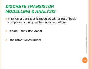
DISCRETE TRANSISTOR
MODELLING & ANALYSIS
 In SPICE, a transistor is modeled with a set of basic
components using mathematical equations.
 Tabular Transistor Model
 Transistor Switch Model
10
--------------------------NIT
Hamirpur--------------
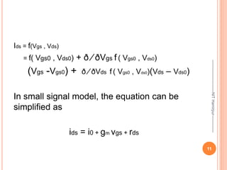
Ids = f(Vgs , Vds)
= f( Vgs0 , Vds0) + ð ⁄ ðVgs f ( Vgs0 , Vds0)
(Vgs -Vgs0) + ð ⁄ ðVds f ( Vgs0 , Vds0)(Vds – Vds0)
In small signal model, the equation can be
simplified as
ids = i0 + gm vgs + rds
--------------------------NIT
Hamirpur--------------
11
TABULAR TRANSISTOR MODEL
 Speed up computation.
 The system was mainly designed for timing and
power analysis of digital circuits.
 It applies the event-driven approach, in which an
event is registered when significant change in node
voltage occurs.
 DC convergence problem
--------------------------NIT
Hamirpur--------------
12
TABULAR TRANSISTOR MODEL
 DC convergence problem
 Transistor model quantization process introduces
inaccuracies
 The maximum circuit size and analysis speed using
the tabular transistor model improves nearly two
orders of magnitude compared to SPICE.
--------------------------NIT
Hamirpur--------------
13
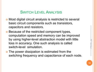
SWITCH LEVEL ANALYSIS
 Most digital circuit analysis is restricted to several
basic circuit components such as transistors,
capacitors and resistors.
 Because of the restricted component types,
computation speed and memory can be improved
by using higher-level abstraction model with little
loss in accuracy. One such analysis is called
switch-level simulation.
 The power dissipation is estimated from the
switching frequency and capacitance of each node.
--------------------------NIT
Hamirpur--------------
14
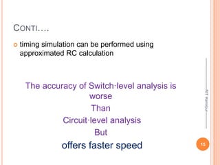
CONTI….
 timing simulation can be performed using
approximated RC calculation
The accuracy of Switch·level analysis is
worse
Than
Circuit·level analysis
But
offers faster speed 15
--------------------------NIT
Hamirpur--------------
GATE LEVEL LOGIC SIMULATION
 The component abstraction at this level is logic
gates and nets.
 The circuit consists of components having defined
logic behavior at its inputs and outputs,
 E.g. NAND gates, latches and flip-flops.
 Most Gate-Level analysis can also handle
capacitors and some can also handle resistors and
restricted models of interconnect wires.
https://www.linkedin.com/pulse/gate-level-simulation-
comprehensive-overview-jerry-mcgoveran/
--------------------------NIT
Hamirpur--------------
16
BASICS OF GATE LEVEL ANALYSIS
 The most popular gate-level analysis is based on
the so called event-driven logic simulation.
 Events are zero-one logic switching of nets
 one switching event occurs at the input of a logic
gate, it may trigger other events at the output of the
gate after a specified time delay
 Most gate-level simulation also supports other logic
states such as, “un known”, “don’t care” and “high-
impedence”.
--------------------------NIT
Hamirpur--------------
17
Verilog and VHDL are two popular languages used to
describe gate-level design
CYCLE-BASED SIMULATORS
 In cycle simulation, it is not possible to specify delays.
 A cycle-accurate model is used, and every gate is
evaluated in every cycle.
 Cycle simulation therefore runs at a constant speed,
regardless of activity in the model.
 Optimized implementations may take advantage of low
model activity to speed up simulation by skipping
evaluation of gates whose inputs didn't change.
 In comparison to event simulation, cycle simulation
tends to be faster, to scale better, and to be better suited
for hardware acceleration / emulation.
18
--------------------------NIT
Hamirpur--------------
HARDWARE ACCELERATION TECHNOLOGY
 Instead of using a general purpose CPU to execute
the simulation program, special purpose hardware
optimized for logic simulation is used.
 This hardware acceleration technology generally
results in several factors of speedup compared to
using a general purpose computing system.
19
--------------------------NIT
Hamirpur--------------
HARDWARE EMULATION
 Several orders of magnitude speedup in gate-level
analysis
 Instead of simulating switching events using software
programs, the logic network is partitioned into smaller
manageable subblocks.
 The Boolean function of each sub-block is extracted
and implemented with a hardware table mapping
mechanism such as RAM or FPGA.
 A reconfigurable interconnection network, carrying the
logic signals, binds the sub-blocks together.
20
--------------------------NIT
Hamirpur--------------
HARDWARE EMULATION
 Circuits up to a million gates can be emulated with
this technology but this is also the most expensive
type of logic simulator to operate and maintain
because of the sophisticated high-speed hardware
required.
 The simulation speed is only one to two orders of
magnitude slower than the actual VLSI chips to be
fabricated.
For example
 200MHz CPU can be emulated with a 2MHz clock
rate, permitting moderate realtime simulation.
21
--------------------------NIT
Hamirpur--------------
CAPACITIVE POWER DISSIPATION
 A major advantage of gate-level power analysis is
that the P=CV2f equation can be computed
precisely and easily.
 The power dissipated due to charging and
discharging capacitors can be easily computed
each in a type of a gate level circuit is associated
with capacitance ci counter variable ti.
 At the end of the simulation, the frequency of net i
is given by fi = ti /(2T), where T is the simulation
time elapsed.
 The capacitive power dissipation of the circuit is
Pcap = i
net
i
i f
V
C
.
2
--------------------------NIT
Hamirpur--------------
22
INTERNAL SWITCHING ENERGY
 The dynamic power dissipated inside the logic cell is
called internal power, which consist of short circuit
power and charging/discharging of internal nodes.
 The computation is repeated for all events of all gates
in the circuit to obtained the total dynamic internal
power dissipation as follows
--------------------------NIT
Hamirpur--------------
23
In the above equation, E(g,e) is the energy of the event e
of gate g obtained from logic gates characterization and
f(g,e) is the occurrence frequency of the event on the gate
observed from logic simulation.
 For a simple logic gate, the internal power
consumed by the gate can be computed through a
characterization process similar to that of timing
analysis for logic gates
 Simulate the "dynamic energy dissipation events" of
the gate with SPICE or other lower-level power
simulation tools.
--------------------------NIT
Hamirpur--------------
24
Dynamic energy dissipation events of a two input CMOS NAND
gate.
A B Y Dyn
Energy(pJ)
1 r f 1.67
1 f r 1.39
r 1 f 1.94
f 1 r 1.72
--------------------------NIT
Hamirpur--------------
25
E (g,e) depends on process conditions, operating voltage, temperature,
output loading capacitance, input signal slopes, etc.
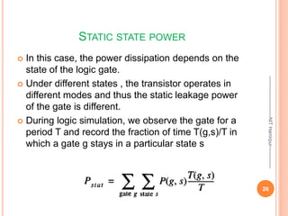
STATIC STATE POWER
 In this case, the power dissipation depends on the
state of the logic gate.
 Under different states , the transistor operates in
different modes and thus the static leakage power
of the gate is different.
 During logic simulation, we observe the gate for a
period T and record the fraction of time T(g,s)/T in
which a gate g stays in a particular state s
--------------------------NIT
Hamirpur--------------
26
A B Y Static
power(pW)
0 0 1 5.05
0 1 1 13.1
1 0 1 5.10
1 1 0 28.5
Static power dissipation states of a two input CMOS NAND gate.
--------------------------NIT
Hamirpur--------------
27
Static State Power
GATE LEVEL CAPACITANCE ESTIMATION
 Capacitance also has a direct impact on delays and
signals slopes of logic gates and influence power
dissipation.
 Two types of parasitic capacitance exist in CMOS
circuit:
1. Device parasitic capacitance
2. Wiring capacitance
 The gate capacitance is heavily dependent on the
oxide thickness of the gate i.e., process dependent.
 Wiring capacitance depends on the layer, area &
shape of the wire.
--------------------------NIT
Hamirpur--------------
28
GATE LEVEL POWER ANALYSIS
 The total power dissipation of the circuit is the sum of
three power components expressed in equation as
follows
P = Pcap + Pint + Pstat
 The analysis speed of gate level tool is fast enough to
allow full chip simulation.
 With the static and internal power characterization, the
accuracy with in 10-15% of SPICE simulation is
possible.
 A major disadvantage of gate level analysis is that signal
glitches cannot be modeled precisely. Signal glitches
can be significant source of power dissipation in VLSI
circuit.
--------------------------NIT
Hamirpur--------------
29
 https://en.wikipedia.org/wiki/List_of_HDL_simulator
s
30
--------------------------NIT
Hamirpur--------------
ARCHITECTURE
LEVEL ANALYSIS
31
--------------------------NIT
Hamirpur--------------
Architecture-Level Analysis
Block level or macro-level design.
The basic building blocks at this level are
register, adders, multipliers, busses,
multiplexers, memories etc.
--------------------------NIT
Hamirpur--------------
32
Architecture-Level Analysis
The dynamic event and static state
characterization method for logic gates cannot
be practically applied to the architectural
components because there are too many events
and states
 16-bit adder
The power dissipation is depending on the logic
values of the inputs.
In the worst case, we may need to enumerate
2 (16+ 16) (4.29 billion) possible events
to fully characterize the 16-bit adder with the
gate-level characterization method.
The enumeration is finite but certainly not
practical to compute.
--------------------------NIT
Hamirpur--------------
33
Power Model Based on Activities
 Well structured regularity.
 The components are typically constructed
by cascading or repeating simpler units built
from logic gates.
One way to characterize the architectural
components is to express the power
dissipation as a function of the number of
bits of the components and their operating
frequencies
--------------------------NIT
Hamirpur--------------
34
Example
The power dissipation of an adder can be
expressed as
P=(nK1 + K2 )f
 where n is the no. of bits, f is the frequency of
addition operation,
 K1 and K2 are empirical coefficients
derived from characterization with a lower-
level power analysis such as gate-level
simulation.
 The model does not take into account the
data dependency of the power dissipation.
--------------------------NIT
Hamirpur--------------
35
CONTI…
 More Accurate Model
 perform characterization to derive the coefficients Ki
 the number of coefficients can be reduced because of
the particular characteristics of the component.
Ai and Bi (ith Bit Position)
For larger components with deep logic
nesting, e.g., multipliers,
36
--------------------------NIT
Hamirpur--------------
CONTI…
 For larger components with deep logic nesting, e.g.,
multipliers,
37
--------------------------NIT
Hamirpur--------------
POWER MODEL BASED ON COMPONENT
OPERATIONS
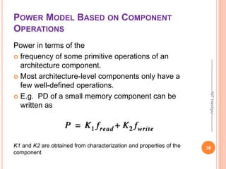
Power in terms of the
 frequency of some primitive operations of an
architecture component.
 Most architecture-level components only have a
few well-defined operations.
 E.g. PD of a small memory component can be
written as
38
--------------------------NIT
Hamirpur--------------
K1 and K2 are obtained from characterization and properties of the
component
CONTI…
 Power dissipation of the READ and WRITE operations of
a memory component is also dependent on the actual
address and data values.
 compromise is to use the average READ and WRITE
energy of the operations
 inaccuracies, but improves the computation efficiency
and generality of the power model.
 If the address and data values of the memory operations
are fairly random, this solution is often very effective in
practice.
39
--------------------------NIT
Hamirpur--------------
CONTI….
 the memory access pattern is skewed such that most of
the READ and WRITE operations occur at a particular
location, e.g., address zero.
40
--------------------------NIT
Hamirpur--------------
DATA CORRELATION ANALYSIS IN DSP
SYSTEMS
 sample correlation has been observed.
 Sample correlation refers to the property that successive
data samples are very close in their numerical values and
consequently their binary representations have many bits
in common.
 001000001 00100011 001000101
41
--------------------------NIT
Hamirpur--------------
CONTI…
 positive or negative correlation has a significant effect
on the power dissipation of a DSP system because of
the switching activities on the system datapath.
 If we can find the relationship between the data
correlation and power dissipation, we can develop a
high-level power model without a sample-by-sample
analysis of the data stream.
 Goal is to estimate power dissipation of an
architecture-level component based on the
frequency and some correlation measures of
the data stream.
42
--------------------------NIT
Hamirpur--------------
DUAL BIT TYPE SIGNAL MODEL
 Toggle characteristics of the data signals under the
influence of data correlation.
 If the data sample is positively correlated,
successive data sample values are very close in
their binary representation.
 This means that the least significant bits (LSB) of
the data bus toggle frequently while the most
significant bits (MSB) are relatively quiet.
43
--------------------------NIT
Hamirpur--------------
 Some of the LSB bits toggle at approximately
half the maximum frequency. This is called the
uniform white noise region because the bits toggle in
a random fashion.
 On the MSB side, the bits have a very low toggle
rate and they are called the sign bit region.
 There is also a grey area between the two regions
where the toggle frequency changes from white
noise to sign bit.
 In this region, the bit-toggle rate changes from near
zero to 0.5, typically in a linear fashion.
44
--------------------------NIT
Hamirpur--------------
EFFECTS OF DATA CORRELATION ON BIT
SWITCHING FREQUENCY
45
--------------------------NIT
Hamirpur--------------
DUAL BIT TYPE MODEL
 1. Sample frequency.
 2. Data correlation factor from -1.0 to + 1.0.
 3. The sign bit and uniform white noise regions with
two integers.
46
--------------------------NIT
Hamirpur--------------
DATAPATH MODULE CHARACTERIZATION AND
POWER ANALYSIS
 The dual bit type signal model provides a very compact
representation of the switching characteristics.
 Develop power dissipation models (equations) under
such signal excitation (power analysis of architectural
components.)
 The power models are sensitive to the signal correlation
and the "bit type" of the signals.
47
--------------------------NIT
Hamirpur--------------
EXAMPLE
Module : single-input single-output block FIFO data
queue.
Assumtions
 There is no activity coupling between any two-bit pair
(single bit of the component and generalize it to the
entire module).
 Lower-level power analysis tool, such as a gate-level
tool, to analyse the power dissipation
48
--------------------------NIT
Hamirpur--------------
CONTI…
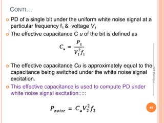
 PD of a single bit under the uniform white noise signal at a
particular frequency f1 & voltage V1
 The effective capacitance C u of the bit is defined as
 The effective capacitance Cu is approximately equal to the
capacitance being switched under the white noise signal
excitation.
 This effective capacitance is used to compute PD under
white noise signal excitation:::::
49
--------------------------NIT
Hamirpur--------------
CONTI….
 The concept of effective capacitance can also be used
on the module bits under the sign bit signal excitation.
 Effective capacitance is no longer a scalar quantity.
 Between successive data samples, the sign bit may or
may not change sign.
 Thus, Four effective capacitance values:
C++ , C+ _, C_+, C_ _
subscript sign pairs
 In a FIFO data queue, it is most likely that
C +_ = C_+ and C++ = C_ _
50
--------------------------NIT
Hamirpur--------------
CONTI..
 construct circuits in which all four effective capacitance
variables have different values.
 With the four effective capacitance values characterized
by a lower-level power analysis tool,
 Construct a power equation.
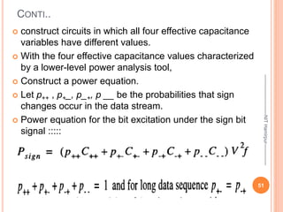
 Let p++ , p+_, p_+, p __ be the probabilities that sign
changes occur in the data stream.
 Power equation for the bit excitation under the sign bit
signal :::::
51
--------------------------NIT
Hamirpur--------------
N-BIT MODULE
 For a module that consists of multiple bits
 Distinguish the white noise bits from the sign bits.
 Take the midpoint of the grey area
 All bits to the left (right) of the midpoint are considered
to have sign bit (white noise) signals.
 Ns =sign bits Nu= white noise bits
 The power dissipation P of the module:::::
52
--------------------------NIT
Hamirpur--------------
 Obtained through Correlation factor and signal
properties of Data stream
 Positive Correlation
53
--------------------------NIT
Hamirpur--------------
 assumes that there are no interactions among data
bits in the module and allows us to characterization
one bit and applies the effective capacitance to the
other bits.
 For modules that have interactions among data bits
 such as barrel shifters. One way to solve this is to
perform the characterization for all
 possible combinations of Nu and Ns. Since Nu + Ns
is equal to the number of bits N
 of the module, there are only N + I conditions to be
characterized. 54
--------------------------NIT
Hamirpur--------------
ADDER MODULE
 The two inputs may have different sign and noise
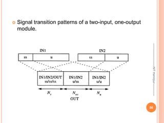
bit separation points.
 This creates a region at the output of the adder in
which the sign and noise bit signals overlap.
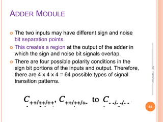
 There are four possible polarity conditions in the
sign bit portions of the inputs and output. Therefore,
there are 4 x 4 x 4 = 64 possible types of signal
transition patterns.
55
--------------------------NIT
Hamirpur--------------
 Signal transition patterns of a two-input, one-output
module.
56
--------------------------NIT
Hamirpur--------------
CONTI…
57
--------------------------NIT
Hamirpur--------------
The "u/ss" condition (INI has noise bits and IN2 has sign
bits) requires another four effective capacitances
The "ss/u“ condition.
The "u/u" input combination only requires one effective
capacitance value.
 Total, 64 + 4 + 4 + I = 73 effective capacitance
values to be characterized using a lower-level
power analysis tool.
MONTE CARLO SIMULATION
58
--------------------------NIT
Hamirpur--------------
59
The future belongs to
those----
Who believe in the beauty
of their dreams

More Related Content

What's hot

EC6601 VLSI Design Memory Circuits
EC6601 VLSI Design   Memory CircuitsEC6601 VLSI Design   Memory Circuits
EC6601 VLSI Design Memory Circuits
chitrarengasamy
 
fpga programming
fpga programmingfpga programming
fpga programmingAnish Gupta
 
System partitioning in VLSI and its considerations
System partitioning in VLSI and its considerationsSystem partitioning in VLSI and its considerations
System partitioning in VLSI and its considerationsSubash John
 
FPGA
FPGAFPGA
Power dissipation cmos
Power dissipation cmosPower dissipation cmos
Power dissipation cmos
Rajesh Tiwary
 
Logic Level Techniques for Power Reduction
Logic Level Techniques for Power Reduction Logic Level Techniques for Power Reduction
Logic Level Techniques for Power Reduction
GargiKhanna1
 
System On Chip (SOC)
System On Chip (SOC)System On Chip (SOC)
System On Chip (SOC)Shivam Gupta
 
Low power vlsi design ppt
Low power vlsi design pptLow power vlsi design ppt
Low power vlsi design ppt
Anil Yadav
 
Reversible Logic Gate
Reversible Logic GateReversible Logic Gate
Reversible Logic Gate
Aneesh Raveendran
 
Low Power Design Approach in VLSI
Low Power Design Approach in VLSILow Power Design Approach in VLSI
Low Power Design Approach in VLSI
Silicon Mentor
 
Fpga architectures and applications
Fpga architectures and applicationsFpga architectures and applications
Fpga architectures and applications
Sudhanshu Janwadkar
 
Pipelining approach
Pipelining approachPipelining approach
Pipelining approach
GopinathD17
 
System On Chip
System On ChipSystem On Chip
System On Chipanishgoel
 
Design of IIR filters
Design of IIR filtersDesign of IIR filters
Design of IIR filters
op205
 
Power Gating
Power GatingPower Gating
Power Gating
Mahesh Dananjaya
 
CMOS LOGIC STRUCTURES
CMOS LOGIC STRUCTURESCMOS LOGIC STRUCTURES
CMOS LOGIC STRUCTURES
VaishaliVaishali14
 
Pass Transistor Logic
Pass Transistor LogicPass Transistor Logic
Pass Transistor LogicDiwaker Pant
 
Fpga
FpgaFpga
Logic synthesis,flootplan&placement
Logic synthesis,flootplan&placementLogic synthesis,flootplan&placement
Logic synthesis,flootplan&placement
shaik sharief
 

What's hot (20)

EC6601 VLSI Design Memory Circuits
EC6601 VLSI Design   Memory CircuitsEC6601 VLSI Design   Memory Circuits
EC6601 VLSI Design Memory Circuits
 
fpga programming
fpga programmingfpga programming
fpga programming
 
Low power vlsi design
Low power vlsi designLow power vlsi design
Low power vlsi design
 
System partitioning in VLSI and its considerations
System partitioning in VLSI and its considerationsSystem partitioning in VLSI and its considerations
System partitioning in VLSI and its considerations
 
FPGA
FPGAFPGA
FPGA
 
Power dissipation cmos
Power dissipation cmosPower dissipation cmos
Power dissipation cmos
 
Logic Level Techniques for Power Reduction
Logic Level Techniques for Power Reduction Logic Level Techniques for Power Reduction
Logic Level Techniques for Power Reduction
 
System On Chip (SOC)
System On Chip (SOC)System On Chip (SOC)
System On Chip (SOC)
 
Low power vlsi design ppt
Low power vlsi design pptLow power vlsi design ppt
Low power vlsi design ppt
 
Reversible Logic Gate
Reversible Logic GateReversible Logic Gate
Reversible Logic Gate
 
Low Power Design Approach in VLSI
Low Power Design Approach in VLSILow Power Design Approach in VLSI
Low Power Design Approach in VLSI
 
Fpga architectures and applications
Fpga architectures and applicationsFpga architectures and applications
Fpga architectures and applications
 
Pipelining approach
Pipelining approachPipelining approach
Pipelining approach
 
System On Chip
System On ChipSystem On Chip
System On Chip
 
Design of IIR filters
Design of IIR filtersDesign of IIR filters
Design of IIR filters
 
Power Gating
Power GatingPower Gating
Power Gating
 
CMOS LOGIC STRUCTURES
CMOS LOGIC STRUCTURESCMOS LOGIC STRUCTURES
CMOS LOGIC STRUCTURES
 
Pass Transistor Logic
Pass Transistor LogicPass Transistor Logic
Pass Transistor Logic
 
Fpga
FpgaFpga
Fpga
 
Logic synthesis,flootplan&placement
Logic synthesis,flootplan&placementLogic synthesis,flootplan&placement
Logic synthesis,flootplan&placement
 

Similar to Simulation power analysis low power vlsi

Real Time System Validation using Hardware in Loop (HIL) Digital Platform
Real Time System Validation using Hardware in Loop (HIL) Digital PlatformReal Time System Validation using Hardware in Loop (HIL) Digital Platform
Real Time System Validation using Hardware in Loop (HIL) Digital Platform
SHIMI S L
 
Implementation of CAN on FPGA for Security Evaluation Purpose
Implementation of CAN on FPGA for Security Evaluation PurposeImplementation of CAN on FPGA for Security Evaluation Purpose
Implementation of CAN on FPGA for Security Evaluation Purpose
IRJET Journal
 
Overview of RTaW SysML-Companion
Overview of RTaW SysML-Companion Overview of RTaW SysML-Companion
Overview of RTaW SysML-Companion
RealTime-at-Work (RTaW)
 
Fpg as 11 body
Fpg as 11 bodyFpg as 11 body
Fpg as 11 body
Rameez Raja
 
C041221821
C041221821C041221821
C041221821
IOSR-JEN
 
Design & implementation of 16 bit low power ALU with clock gating
Design & implementation of 16 bit low power ALU with clock gatingDesign & implementation of 16 bit low power ALU with clock gating
Design & implementation of 16 bit low power ALU with clock gating
IRJET Journal
 
[IJET-V1I3P5] Authors :Dushyant Kumar Soni, Ashish Hiradhar
[IJET-V1I3P5] Authors :Dushyant Kumar Soni, Ashish Hiradhar[IJET-V1I3P5] Authors :Dushyant Kumar Soni, Ashish Hiradhar
[IJET-V1I3P5] Authors :Dushyant Kumar Soni, Ashish Hiradhar
IJET - International Journal of Engineering and Techniques
 
Circuit Level Modelling Simulink Projects Research Help
Circuit Level Modelling Simulink Projects Research HelpCircuit Level Modelling Simulink Projects Research Help
Circuit Level Modelling Simulink Projects Research Help
Matlab Simulation
 
Seminar on field programmable gate array
Seminar on field programmable gate arraySeminar on field programmable gate array
Seminar on field programmable gate array
Saransh Choudhary
 
01 introduction to_plc-pac_rev01_fa16
01 introduction to_plc-pac_rev01_fa1601 introduction to_plc-pac_rev01_fa16
01 introduction to_plc-pac_rev01_fa16
John Todora
 
OPAL-RT Real time simulation using RT-LAB
OPAL-RT Real time simulation using RT-LABOPAL-RT Real time simulation using RT-LAB
OPAL-RT Real time simulation using RT-LAB
OPAL-RT TECHNOLOGIES
 
Plc Paper Presentation By Durreshahwar
Plc Paper Presentation By DurreshahwarPlc Paper Presentation By Durreshahwar
Plc Paper Presentation By Durreshahwar
IEEEP Karachi
 
Research Inventy: International Journal of Engineering and Science
Research Inventy: International Journal of Engineering and ScienceResearch Inventy: International Journal of Engineering and Science
Research Inventy: International Journal of Engineering and Scienceresearchinventy
 
Research Inventy : International Journal of Engineering and Science is publis...
Research Inventy : International Journal of Engineering and Science is publis...Research Inventy : International Journal of Engineering and Science is publis...
Research Inventy : International Journal of Engineering and Science is publis...researchinventy
 
Implementation of T-Junction Traffic Light Control System Using Simatic S7-20...
Implementation of T-Junction Traffic Light Control System Using Simatic S7-20...Implementation of T-Junction Traffic Light Control System Using Simatic S7-20...
Implementation of T-Junction Traffic Light Control System Using Simatic S7-20...
IJERA Editor
 
CodeWarrior, Linux; OrCad and Hyperlynx; QMS Tools
CodeWarrior, Linux; OrCad and Hyperlynx; QMS ToolsCodeWarrior, Linux; OrCad and Hyperlynx; QMS Tools
CodeWarrior, Linux; OrCad and Hyperlynx; QMS Toolsdjerrybellott
 
Program, Code of Program and Screen Shot of Output (UNIVERSAL DRIVER USING µ...
Program, Code of Program and  Screen Shot of Output (UNIVERSAL DRIVER USING µ...Program, Code of Program and  Screen Shot of Output (UNIVERSAL DRIVER USING µ...
Program, Code of Program and Screen Shot of Output (UNIVERSAL DRIVER USING µ...
Er. Ashish Pandey
 
RT15 Berkeley | Introduction to FPGA Power Electronic & Electric Machine real...
RT15 Berkeley | Introduction to FPGA Power Electronic & Electric Machine real...RT15 Berkeley | Introduction to FPGA Power Electronic & Electric Machine real...
RT15 Berkeley | Introduction to FPGA Power Electronic & Electric Machine real...
OPAL-RT TECHNOLOGIES
 

Similar to Simulation power analysis low power vlsi (20)

Real Time System Validation using Hardware in Loop (HIL) Digital Platform
Real Time System Validation using Hardware in Loop (HIL) Digital PlatformReal Time System Validation using Hardware in Loop (HIL) Digital Platform
Real Time System Validation using Hardware in Loop (HIL) Digital Platform
 
Implementation of CAN on FPGA for Security Evaluation Purpose
Implementation of CAN on FPGA for Security Evaluation PurposeImplementation of CAN on FPGA for Security Evaluation Purpose
Implementation of CAN on FPGA for Security Evaluation Purpose
 
Overview of RTaW SysML-Companion
Overview of RTaW SysML-Companion Overview of RTaW SysML-Companion
Overview of RTaW SysML-Companion
 
Fpg as 11 body
Fpg as 11 bodyFpg as 11 body
Fpg as 11 body
 
C041221821
C041221821C041221821
C041221821
 
Design & implementation of 16 bit low power ALU with clock gating
Design & implementation of 16 bit low power ALU with clock gatingDesign & implementation of 16 bit low power ALU with clock gating
Design & implementation of 16 bit low power ALU with clock gating
 
[IJET-V1I3P5] Authors :Dushyant Kumar Soni, Ashish Hiradhar
[IJET-V1I3P5] Authors :Dushyant Kumar Soni, Ashish Hiradhar[IJET-V1I3P5] Authors :Dushyant Kumar Soni, Ashish Hiradhar
[IJET-V1I3P5] Authors :Dushyant Kumar Soni, Ashish Hiradhar
 
Circuit Level Modelling Simulink Projects Research Help
Circuit Level Modelling Simulink Projects Research HelpCircuit Level Modelling Simulink Projects Research Help
Circuit Level Modelling Simulink Projects Research Help
 
Seminar on field programmable gate array
Seminar on field programmable gate arraySeminar on field programmable gate array
Seminar on field programmable gate array
 
01 introduction to_plc-pac_rev01_fa16
01 introduction to_plc-pac_rev01_fa1601 introduction to_plc-pac_rev01_fa16
01 introduction to_plc-pac_rev01_fa16
 
OPAL-RT Real time simulation using RT-LAB
OPAL-RT Real time simulation using RT-LABOPAL-RT Real time simulation using RT-LAB
OPAL-RT Real time simulation using RT-LAB
 
Asic
AsicAsic
Asic
 
Plc Paper Presentation By Durreshahwar
Plc Paper Presentation By DurreshahwarPlc Paper Presentation By Durreshahwar
Plc Paper Presentation By Durreshahwar
 
Research Inventy: International Journal of Engineering and Science
Research Inventy: International Journal of Engineering and ScienceResearch Inventy: International Journal of Engineering and Science
Research Inventy: International Journal of Engineering and Science
 
Research Inventy : International Journal of Engineering and Science is publis...
Research Inventy : International Journal of Engineering and Science is publis...Research Inventy : International Journal of Engineering and Science is publis...
Research Inventy : International Journal of Engineering and Science is publis...
 
Implementation of T-Junction Traffic Light Control System Using Simatic S7-20...
Implementation of T-Junction Traffic Light Control System Using Simatic S7-20...Implementation of T-Junction Traffic Light Control System Using Simatic S7-20...
Implementation of T-Junction Traffic Light Control System Using Simatic S7-20...
 
Dp32725728
Dp32725728Dp32725728
Dp32725728
 
CodeWarrior, Linux; OrCad and Hyperlynx; QMS Tools
CodeWarrior, Linux; OrCad and Hyperlynx; QMS ToolsCodeWarrior, Linux; OrCad and Hyperlynx; QMS Tools
CodeWarrior, Linux; OrCad and Hyperlynx; QMS Tools
 
Program, Code of Program and Screen Shot of Output (UNIVERSAL DRIVER USING µ...
Program, Code of Program and  Screen Shot of Output (UNIVERSAL DRIVER USING µ...Program, Code of Program and  Screen Shot of Output (UNIVERSAL DRIVER USING µ...
Program, Code of Program and Screen Shot of Output (UNIVERSAL DRIVER USING µ...
 
RT15 Berkeley | Introduction to FPGA Power Electronic & Electric Machine real...
RT15 Berkeley | Introduction to FPGA Power Electronic & Electric Machine real...RT15 Berkeley | Introduction to FPGA Power Electronic & Electric Machine real...
RT15 Berkeley | Introduction to FPGA Power Electronic & Electric Machine real...
 

More from GargiKhanna1

Latch & Flip-Flop.pptx
Latch & Flip-Flop.pptxLatch & Flip-Flop.pptx
Latch & Flip-Flop.pptx
GargiKhanna1
 
MOS logic family
MOS logic familyMOS logic family
MOS logic family
GargiKhanna1
 
Digital Counter Design
 Digital Counter Design Digital Counter Design
Digital Counter Design
GargiKhanna1
 
Latch and flip flop
Latch and flip flopLatch and flip flop
Latch and flip flop
GargiKhanna1
 
Multiplexers and Demultiplexers
Multiplexers and DemultiplexersMultiplexers and Demultiplexers
Multiplexers and Demultiplexers
GargiKhanna1
 
Combinational Logic Circuit
Combinational Logic CircuitCombinational Logic Circuit
Combinational Logic Circuit
GargiKhanna1
 
Karnaugh Map
Karnaugh MapKarnaugh Map
Karnaugh Map
GargiKhanna1
 
Error detection and correction codes
Error detection and correction codesError detection and correction codes
Error detection and correction codes
GargiKhanna1
 
Number system
Number system Number system
Number system
GargiKhanna1
 
Boolean Function SOP & POS
Boolean Function SOP &  POSBoolean Function SOP &  POS
Boolean Function SOP & POS
GargiKhanna1
 
Logic gate
Logic gateLogic gate
Logic gate
GargiKhanna1
 
Logic Gates
Logic GatesLogic Gates
Logic Gates
GargiKhanna1
 
Binary codes
Binary codesBinary codes
Binary codes
GargiKhanna1
 
Binary Arithmetic
Binary ArithmeticBinary Arithmetic
Binary Arithmetic
GargiKhanna1
 

More from GargiKhanna1 (14)

Latch & Flip-Flop.pptx
Latch & Flip-Flop.pptxLatch & Flip-Flop.pptx
Latch & Flip-Flop.pptx
 
MOS logic family
MOS logic familyMOS logic family
MOS logic family
 
Digital Counter Design
 Digital Counter Design Digital Counter Design
Digital Counter Design
 
Latch and flip flop
Latch and flip flopLatch and flip flop
Latch and flip flop
 
Multiplexers and Demultiplexers
Multiplexers and DemultiplexersMultiplexers and Demultiplexers
Multiplexers and Demultiplexers
 
Combinational Logic Circuit
Combinational Logic CircuitCombinational Logic Circuit
Combinational Logic Circuit
 
Karnaugh Map
Karnaugh MapKarnaugh Map
Karnaugh Map
 
Error detection and correction codes
Error detection and correction codesError detection and correction codes
Error detection and correction codes
 
Number system
Number system Number system
Number system
 
Boolean Function SOP & POS
Boolean Function SOP &  POSBoolean Function SOP &  POS
Boolean Function SOP & POS
 
Logic gate
Logic gateLogic gate
Logic gate
 
Logic Gates
Logic GatesLogic Gates
Logic Gates
 
Binary codes
Binary codesBinary codes
Binary codes
 
Binary Arithmetic
Binary ArithmeticBinary Arithmetic
Binary Arithmetic
 

Recently uploaded

Water Industry Process Automation and Control Monthly - May 2024.pdf
Water Industry Process Automation and Control Monthly - May 2024.pdfWater Industry Process Automation and Control Monthly - May 2024.pdf
Water Industry Process Automation and Control Monthly - May 2024.pdf
Water Industry Process Automation & Control
 
CFD Simulation of By-pass Flow in a HRSG module by R&R Consult.pptx
CFD Simulation of By-pass Flow in a HRSG module by R&R Consult.pptxCFD Simulation of By-pass Flow in a HRSG module by R&R Consult.pptx
CFD Simulation of By-pass Flow in a HRSG module by R&R Consult.pptx
R&R Consult
 
J.Yang, ICLR 2024, MLILAB, KAIST AI.pdf
J.Yang,  ICLR 2024, MLILAB, KAIST AI.pdfJ.Yang,  ICLR 2024, MLILAB, KAIST AI.pdf
J.Yang, ICLR 2024, MLILAB, KAIST AI.pdf
MLILAB
 
Democratizing Fuzzing at Scale by Abhishek Arya
Democratizing Fuzzing at Scale by Abhishek AryaDemocratizing Fuzzing at Scale by Abhishek Arya
Democratizing Fuzzing at Scale by Abhishek Arya
abh.arya
 
Standard Reomte Control Interface - Neometrix
Standard Reomte Control Interface - NeometrixStandard Reomte Control Interface - Neometrix
Standard Reomte Control Interface - Neometrix
Neometrix_Engineering_Pvt_Ltd
 
road safety engineering r s e unit 3.pdf
road safety engineering  r s e unit 3.pdfroad safety engineering  r s e unit 3.pdf
road safety engineering r s e unit 3.pdf
VENKATESHvenky89705
 
Forklift Classes Overview by Intella Parts
Forklift Classes Overview by Intella PartsForklift Classes Overview by Intella Parts
Forklift Classes Overview by Intella Parts
Intella Parts
 
block diagram and signal flow graph representation
block diagram and signal flow graph representationblock diagram and signal flow graph representation
block diagram and signal flow graph representation
Divya Somashekar
 
Top 10 Oil and Gas Projects in Saudi Arabia 2024.pdf
Top 10 Oil and Gas Projects in Saudi Arabia 2024.pdfTop 10 Oil and Gas Projects in Saudi Arabia 2024.pdf
Top 10 Oil and Gas Projects in Saudi Arabia 2024.pdf
Teleport Manpower Consultant
 
Design and Analysis of Algorithms-DP,Backtracking,Graphs,B&B
Design and Analysis of Algorithms-DP,Backtracking,Graphs,B&BDesign and Analysis of Algorithms-DP,Backtracking,Graphs,B&B
Design and Analysis of Algorithms-DP,Backtracking,Graphs,B&B
Sreedhar Chowdam
 
Automobile Management System Project Report.pdf
Automobile Management System Project Report.pdfAutomobile Management System Project Report.pdf
Automobile Management System Project Report.pdf
Kamal Acharya
 
Vaccine management system project report documentation..pdf
Vaccine management system project report documentation..pdfVaccine management system project report documentation..pdf
Vaccine management system project report documentation..pdf
Kamal Acharya
 
ASME IX(9) 2007 Full Version .pdf
ASME IX(9)  2007 Full Version       .pdfASME IX(9)  2007 Full Version       .pdf
ASME IX(9) 2007 Full Version .pdf
AhmedHussein950959
 
Hybrid optimization of pumped hydro system and solar- Engr. Abdul-Azeez.pdf
Hybrid optimization of pumped hydro system and solar- Engr. Abdul-Azeez.pdfHybrid optimization of pumped hydro system and solar- Engr. Abdul-Azeez.pdf
Hybrid optimization of pumped hydro system and solar- Engr. Abdul-Azeez.pdf
fxintegritypublishin
 
Planning Of Procurement o different goods and services
Planning Of Procurement o different goods and servicesPlanning Of Procurement o different goods and services
Planning Of Procurement o different goods and services
JoytuBarua2
 
一比一原版(SFU毕业证)西蒙菲莎大学毕业证成绩单如何办理
一比一原版(SFU毕业证)西蒙菲莎大学毕业证成绩单如何办理一比一原版(SFU毕业证)西蒙菲莎大学毕业证成绩单如何办理
一比一原版(SFU毕业证)西蒙菲莎大学毕业证成绩单如何办理
bakpo1
 
The role of big data in decision making.
The role of big data in decision making.The role of big data in decision making.
The role of big data in decision making.
ankuprajapati0525
 
ethical hacking in wireless-hacking1.ppt
ethical hacking in wireless-hacking1.pptethical hacking in wireless-hacking1.ppt
ethical hacking in wireless-hacking1.ppt
Jayaprasanna4
 
weather web application report.pdf
weather web application report.pdfweather web application report.pdf
weather web application report.pdf
Pratik Pawar
 
LIGA(E)11111111111111111111111111111111111111111.ppt
LIGA(E)11111111111111111111111111111111111111111.pptLIGA(E)11111111111111111111111111111111111111111.ppt
LIGA(E)11111111111111111111111111111111111111111.ppt
ssuser9bd3ba
 

Recently uploaded (20)

Water Industry Process Automation and Control Monthly - May 2024.pdf
Water Industry Process Automation and Control Monthly - May 2024.pdfWater Industry Process Automation and Control Monthly - May 2024.pdf
Water Industry Process Automation and Control Monthly - May 2024.pdf
 
CFD Simulation of By-pass Flow in a HRSG module by R&R Consult.pptx
CFD Simulation of By-pass Flow in a HRSG module by R&R Consult.pptxCFD Simulation of By-pass Flow in a HRSG module by R&R Consult.pptx
CFD Simulation of By-pass Flow in a HRSG module by R&R Consult.pptx
 
J.Yang, ICLR 2024, MLILAB, KAIST AI.pdf
J.Yang,  ICLR 2024, MLILAB, KAIST AI.pdfJ.Yang,  ICLR 2024, MLILAB, KAIST AI.pdf
J.Yang, ICLR 2024, MLILAB, KAIST AI.pdf
 
Democratizing Fuzzing at Scale by Abhishek Arya
Democratizing Fuzzing at Scale by Abhishek AryaDemocratizing Fuzzing at Scale by Abhishek Arya
Democratizing Fuzzing at Scale by Abhishek Arya
 
Standard Reomte Control Interface - Neometrix
Standard Reomte Control Interface - NeometrixStandard Reomte Control Interface - Neometrix
Standard Reomte Control Interface - Neometrix
 
road safety engineering r s e unit 3.pdf
road safety engineering  r s e unit 3.pdfroad safety engineering  r s e unit 3.pdf
road safety engineering r s e unit 3.pdf
 
Forklift Classes Overview by Intella Parts
Forklift Classes Overview by Intella PartsForklift Classes Overview by Intella Parts
Forklift Classes Overview by Intella Parts
 
block diagram and signal flow graph representation
block diagram and signal flow graph representationblock diagram and signal flow graph representation
block diagram and signal flow graph representation
 
Top 10 Oil and Gas Projects in Saudi Arabia 2024.pdf
Top 10 Oil and Gas Projects in Saudi Arabia 2024.pdfTop 10 Oil and Gas Projects in Saudi Arabia 2024.pdf
Top 10 Oil and Gas Projects in Saudi Arabia 2024.pdf
 
Design and Analysis of Algorithms-DP,Backtracking,Graphs,B&B
Design and Analysis of Algorithms-DP,Backtracking,Graphs,B&BDesign and Analysis of Algorithms-DP,Backtracking,Graphs,B&B
Design and Analysis of Algorithms-DP,Backtracking,Graphs,B&B
 
Automobile Management System Project Report.pdf
Automobile Management System Project Report.pdfAutomobile Management System Project Report.pdf
Automobile Management System Project Report.pdf
 
Vaccine management system project report documentation..pdf
Vaccine management system project report documentation..pdfVaccine management system project report documentation..pdf
Vaccine management system project report documentation..pdf
 
ASME IX(9) 2007 Full Version .pdf
ASME IX(9)  2007 Full Version       .pdfASME IX(9)  2007 Full Version       .pdf
ASME IX(9) 2007 Full Version .pdf
 
Hybrid optimization of pumped hydro system and solar- Engr. Abdul-Azeez.pdf
Hybrid optimization of pumped hydro system and solar- Engr. Abdul-Azeez.pdfHybrid optimization of pumped hydro system and solar- Engr. Abdul-Azeez.pdf
Hybrid optimization of pumped hydro system and solar- Engr. Abdul-Azeez.pdf
 
Planning Of Procurement o different goods and services
Planning Of Procurement o different goods and servicesPlanning Of Procurement o different goods and services
Planning Of Procurement o different goods and services
 
一比一原版(SFU毕业证)西蒙菲莎大学毕业证成绩单如何办理
一比一原版(SFU毕业证)西蒙菲莎大学毕业证成绩单如何办理一比一原版(SFU毕业证)西蒙菲莎大学毕业证成绩单如何办理
一比一原版(SFU毕业证)西蒙菲莎大学毕业证成绩单如何办理
 
The role of big data in decision making.
The role of big data in decision making.The role of big data in decision making.
The role of big data in decision making.
 
ethical hacking in wireless-hacking1.ppt
ethical hacking in wireless-hacking1.pptethical hacking in wireless-hacking1.ppt
ethical hacking in wireless-hacking1.ppt
 
weather web application report.pdf
weather web application report.pdfweather web application report.pdf
weather web application report.pdf
 
LIGA(E)11111111111111111111111111111111111111111.ppt
LIGA(E)11111111111111111111111111111111111111111.pptLIGA(E)11111111111111111111111111111111111111111.ppt
LIGA(E)11111111111111111111111111111111111111111.ppt
 

Simulation power analysis low power vlsi

  • 1. SIMULATION POWER ANALYSIS NATIONAL INSTITUTE OF TECHNOLOGY HAMIRPUR Presented By Dr. Gargi Khanna Associate Professor E&CED Dept. , NIT Hamirpur, HP.
  • 2. INTRODUCTION  Simulation is…. Modeling of a design, its function and performance Imitate the operation of a facility or process via computer  is used to:  Verify the functionality and correctness of design  Estimate the performance (Speed , Power)  Verify the test  Estimation of cost  Reliability analysis.  To represent the system in software --------------------------NIT Hamirpur-------------- 2
  • 4. COMPUTING RESOURCES AND ANALYSIS ACCURACY AT VARIOUS ABSTRACTION LEVELS Abstraction level Computing resources Analysis accuracy Algorithm Least Worst Software & System Hardware behavior Register transfer(RTL)/Function Level Logic Circuit Device Most Best --------------------------NIT Hamirpur-------------- 4 the trade-off between computing resources and accuracy of resource.
  • 5.  Simulation techniques to estimate and analyze power dissipation of VLSI chips and the concept of characterization will be emphasized.  Characterization refers to the process of using lower level analysis results as a basis to construct higher level power models. --------------------------NIT Hamirpur-------------- 5
  • 8. SPICE CIRCUIT SIMULATION  SPICE is the de facto power analysis tool at the circuit level. SPICE BASICS ::  SPICE operates by solving of nodal current using the Kirchhoff's current law.  SPICE offers several analysis modes but the most useful mode for digital IC power analysis is called “transient analysis”.  SPICE device models are derived from a characterization process.  The models are typically calibrated with physical measurements taken from actual test chips and can achieve a very high degree of accuracy. --------------------------NIT Hamirpur-------------- 8
  • 9. SPICE POWER ANALYSIS  The strongest advantage of SPICE is of cause its accuracy. It can be used to estimate dynamic, static & leakage power dissipation.  SPICE analysis requires intensive computation resources and is thus not suitable for large circuits. :: --------------------------NIT Hamirpur-------------- 9
  • 10. DISCRETE TRANSISTOR MODELLING & ANALYSIS  In SPICE, a transistor is modeled with a set of basic components using mathematical equations.  Tabular Transistor Model  Transistor Switch Model 10 --------------------------NIT Hamirpur--------------
  • 11. Ids = f(Vgs , Vds) = f( Vgs0 , Vds0) + ð ⁄ ðVgs f ( Vgs0 , Vds0) (Vgs -Vgs0) + ð ⁄ ðVds f ( Vgs0 , Vds0)(Vds – Vds0) In small signal model, the equation can be simplified as ids = i0 + gm vgs + rds --------------------------NIT Hamirpur-------------- 11
  • 12. TABULAR TRANSISTOR MODEL  Speed up computation.  The system was mainly designed for timing and power analysis of digital circuits.  It applies the event-driven approach, in which an event is registered when significant change in node voltage occurs.  DC convergence problem --------------------------NIT Hamirpur-------------- 12
  • 13. TABULAR TRANSISTOR MODEL  DC convergence problem  Transistor model quantization process introduces inaccuracies  The maximum circuit size and analysis speed using the tabular transistor model improves nearly two orders of magnitude compared to SPICE. --------------------------NIT Hamirpur-------------- 13
  • 14. SWITCH LEVEL ANALYSIS  Most digital circuit analysis is restricted to several basic circuit components such as transistors, capacitors and resistors.  Because of the restricted component types, computation speed and memory can be improved by using higher-level abstraction model with little loss in accuracy. One such analysis is called switch-level simulation.  The power dissipation is estimated from the switching frequency and capacitance of each node. --------------------------NIT Hamirpur-------------- 14
  • 15. CONTI….  timing simulation can be performed using approximated RC calculation The accuracy of Switch·level analysis is worse Than Circuit·level analysis But offers faster speed 15 --------------------------NIT Hamirpur--------------
  • 16. GATE LEVEL LOGIC SIMULATION  The component abstraction at this level is logic gates and nets.  The circuit consists of components having defined logic behavior at its inputs and outputs,  E.g. NAND gates, latches and flip-flops.  Most Gate-Level analysis can also handle capacitors and some can also handle resistors and restricted models of interconnect wires. https://www.linkedin.com/pulse/gate-level-simulation- comprehensive-overview-jerry-mcgoveran/ --------------------------NIT Hamirpur-------------- 16
  • 17. BASICS OF GATE LEVEL ANALYSIS  The most popular gate-level analysis is based on the so called event-driven logic simulation.  Events are zero-one logic switching of nets  one switching event occurs at the input of a logic gate, it may trigger other events at the output of the gate after a specified time delay  Most gate-level simulation also supports other logic states such as, “un known”, “don’t care” and “high- impedence”. --------------------------NIT Hamirpur-------------- 17 Verilog and VHDL are two popular languages used to describe gate-level design
  • 18. CYCLE-BASED SIMULATORS  In cycle simulation, it is not possible to specify delays.  A cycle-accurate model is used, and every gate is evaluated in every cycle.  Cycle simulation therefore runs at a constant speed, regardless of activity in the model.  Optimized implementations may take advantage of low model activity to speed up simulation by skipping evaluation of gates whose inputs didn't change.  In comparison to event simulation, cycle simulation tends to be faster, to scale better, and to be better suited for hardware acceleration / emulation. 18 --------------------------NIT Hamirpur--------------
  • 19. HARDWARE ACCELERATION TECHNOLOGY  Instead of using a general purpose CPU to execute the simulation program, special purpose hardware optimized for logic simulation is used.  This hardware acceleration technology generally results in several factors of speedup compared to using a general purpose computing system. 19 --------------------------NIT Hamirpur--------------
  • 20. HARDWARE EMULATION  Several orders of magnitude speedup in gate-level analysis  Instead of simulating switching events using software programs, the logic network is partitioned into smaller manageable subblocks.  The Boolean function of each sub-block is extracted and implemented with a hardware table mapping mechanism such as RAM or FPGA.  A reconfigurable interconnection network, carrying the logic signals, binds the sub-blocks together. 20 --------------------------NIT Hamirpur--------------
  • 21. HARDWARE EMULATION  Circuits up to a million gates can be emulated with this technology but this is also the most expensive type of logic simulator to operate and maintain because of the sophisticated high-speed hardware required.  The simulation speed is only one to two orders of magnitude slower than the actual VLSI chips to be fabricated. For example  200MHz CPU can be emulated with a 2MHz clock rate, permitting moderate realtime simulation. 21 --------------------------NIT Hamirpur--------------
  • 22. CAPACITIVE POWER DISSIPATION  A major advantage of gate-level power analysis is that the P=CV2f equation can be computed precisely and easily.  The power dissipated due to charging and discharging capacitors can be easily computed each in a type of a gate level circuit is associated with capacitance ci counter variable ti.  At the end of the simulation, the frequency of net i is given by fi = ti /(2T), where T is the simulation time elapsed.  The capacitive power dissipation of the circuit is Pcap = i net i i f V C . 2 --------------------------NIT Hamirpur-------------- 22
  • 23. INTERNAL SWITCHING ENERGY  The dynamic power dissipated inside the logic cell is called internal power, which consist of short circuit power and charging/discharging of internal nodes.  The computation is repeated for all events of all gates in the circuit to obtained the total dynamic internal power dissipation as follows --------------------------NIT Hamirpur-------------- 23
  • 24. In the above equation, E(g,e) is the energy of the event e of gate g obtained from logic gates characterization and f(g,e) is the occurrence frequency of the event on the gate observed from logic simulation.  For a simple logic gate, the internal power consumed by the gate can be computed through a characterization process similar to that of timing analysis for logic gates  Simulate the "dynamic energy dissipation events" of the gate with SPICE or other lower-level power simulation tools. --------------------------NIT Hamirpur-------------- 24
  • 25. Dynamic energy dissipation events of a two input CMOS NAND gate. A B Y Dyn Energy(pJ) 1 r f 1.67 1 f r 1.39 r 1 f 1.94 f 1 r 1.72 --------------------------NIT Hamirpur-------------- 25 E (g,e) depends on process conditions, operating voltage, temperature, output loading capacitance, input signal slopes, etc.
  • 26. STATIC STATE POWER  In this case, the power dissipation depends on the state of the logic gate.  Under different states , the transistor operates in different modes and thus the static leakage power of the gate is different.  During logic simulation, we observe the gate for a period T and record the fraction of time T(g,s)/T in which a gate g stays in a particular state s --------------------------NIT Hamirpur-------------- 26
  • 27. A B Y Static power(pW) 0 0 1 5.05 0 1 1 13.1 1 0 1 5.10 1 1 0 28.5 Static power dissipation states of a two input CMOS NAND gate. --------------------------NIT Hamirpur-------------- 27 Static State Power
  • 28. GATE LEVEL CAPACITANCE ESTIMATION  Capacitance also has a direct impact on delays and signals slopes of logic gates and influence power dissipation.  Two types of parasitic capacitance exist in CMOS circuit: 1. Device parasitic capacitance 2. Wiring capacitance  The gate capacitance is heavily dependent on the oxide thickness of the gate i.e., process dependent.  Wiring capacitance depends on the layer, area & shape of the wire. --------------------------NIT Hamirpur-------------- 28
  • 29. GATE LEVEL POWER ANALYSIS  The total power dissipation of the circuit is the sum of three power components expressed in equation as follows P = Pcap + Pint + Pstat  The analysis speed of gate level tool is fast enough to allow full chip simulation.  With the static and internal power characterization, the accuracy with in 10-15% of SPICE simulation is possible.  A major disadvantage of gate level analysis is that signal glitches cannot be modeled precisely. Signal glitches can be significant source of power dissipation in VLSI circuit. --------------------------NIT Hamirpur-------------- 29
  • 32. Architecture-Level Analysis Block level or macro-level design. The basic building blocks at this level are register, adders, multipliers, busses, multiplexers, memories etc. --------------------------NIT Hamirpur-------------- 32
  • 33. Architecture-Level Analysis The dynamic event and static state characterization method for logic gates cannot be practically applied to the architectural components because there are too many events and states  16-bit adder The power dissipation is depending on the logic values of the inputs. In the worst case, we may need to enumerate 2 (16+ 16) (4.29 billion) possible events to fully characterize the 16-bit adder with the gate-level characterization method. The enumeration is finite but certainly not practical to compute. --------------------------NIT Hamirpur-------------- 33
  • 34. Power Model Based on Activities  Well structured regularity.  The components are typically constructed by cascading or repeating simpler units built from logic gates. One way to characterize the architectural components is to express the power dissipation as a function of the number of bits of the components and their operating frequencies --------------------------NIT Hamirpur-------------- 34
  • 35. Example The power dissipation of an adder can be expressed as P=(nK1 + K2 )f  where n is the no. of bits, f is the frequency of addition operation,  K1 and K2 are empirical coefficients derived from characterization with a lower- level power analysis such as gate-level simulation.  The model does not take into account the data dependency of the power dissipation. --------------------------NIT Hamirpur-------------- 35
  • 36. CONTI…  More Accurate Model  perform characterization to derive the coefficients Ki  the number of coefficients can be reduced because of the particular characteristics of the component. Ai and Bi (ith Bit Position) For larger components with deep logic nesting, e.g., multipliers, 36 --------------------------NIT Hamirpur--------------
  • 37. CONTI…  For larger components with deep logic nesting, e.g., multipliers, 37 --------------------------NIT Hamirpur--------------
  • 38. POWER MODEL BASED ON COMPONENT OPERATIONS Power in terms of the  frequency of some primitive operations of an architecture component.  Most architecture-level components only have a few well-defined operations.  E.g. PD of a small memory component can be written as 38 --------------------------NIT Hamirpur-------------- K1 and K2 are obtained from characterization and properties of the component
  • 39. CONTI…  Power dissipation of the READ and WRITE operations of a memory component is also dependent on the actual address and data values.  compromise is to use the average READ and WRITE energy of the operations  inaccuracies, but improves the computation efficiency and generality of the power model.  If the address and data values of the memory operations are fairly random, this solution is often very effective in practice. 39 --------------------------NIT Hamirpur--------------
  • 40. CONTI….  the memory access pattern is skewed such that most of the READ and WRITE operations occur at a particular location, e.g., address zero. 40 --------------------------NIT Hamirpur--------------
  • 41. DATA CORRELATION ANALYSIS IN DSP SYSTEMS  sample correlation has been observed.  Sample correlation refers to the property that successive data samples are very close in their numerical values and consequently their binary representations have many bits in common.  001000001 00100011 001000101 41 --------------------------NIT Hamirpur--------------
  • 42. CONTI…  positive or negative correlation has a significant effect on the power dissipation of a DSP system because of the switching activities on the system datapath.  If we can find the relationship between the data correlation and power dissipation, we can develop a high-level power model without a sample-by-sample analysis of the data stream.  Goal is to estimate power dissipation of an architecture-level component based on the frequency and some correlation measures of the data stream. 42 --------------------------NIT Hamirpur--------------
  • 43. DUAL BIT TYPE SIGNAL MODEL  Toggle characteristics of the data signals under the influence of data correlation.  If the data sample is positively correlated, successive data sample values are very close in their binary representation.  This means that the least significant bits (LSB) of the data bus toggle frequently while the most significant bits (MSB) are relatively quiet. 43 --------------------------NIT Hamirpur--------------
  • 44.  Some of the LSB bits toggle at approximately half the maximum frequency. This is called the uniform white noise region because the bits toggle in a random fashion.  On the MSB side, the bits have a very low toggle rate and they are called the sign bit region.  There is also a grey area between the two regions where the toggle frequency changes from white noise to sign bit.  In this region, the bit-toggle rate changes from near zero to 0.5, typically in a linear fashion. 44 --------------------------NIT Hamirpur--------------
  • 45. EFFECTS OF DATA CORRELATION ON BIT SWITCHING FREQUENCY 45 --------------------------NIT Hamirpur--------------
  • 46. DUAL BIT TYPE MODEL  1. Sample frequency.  2. Data correlation factor from -1.0 to + 1.0.  3. The sign bit and uniform white noise regions with two integers. 46 --------------------------NIT Hamirpur--------------
  • 47. DATAPATH MODULE CHARACTERIZATION AND POWER ANALYSIS  The dual bit type signal model provides a very compact representation of the switching characteristics.  Develop power dissipation models (equations) under such signal excitation (power analysis of architectural components.)  The power models are sensitive to the signal correlation and the "bit type" of the signals. 47 --------------------------NIT Hamirpur--------------
  • 48. EXAMPLE Module : single-input single-output block FIFO data queue. Assumtions  There is no activity coupling between any two-bit pair (single bit of the component and generalize it to the entire module).  Lower-level power analysis tool, such as a gate-level tool, to analyse the power dissipation 48 --------------------------NIT Hamirpur--------------
  • 49. CONTI…  PD of a single bit under the uniform white noise signal at a particular frequency f1 & voltage V1  The effective capacitance C u of the bit is defined as  The effective capacitance Cu is approximately equal to the capacitance being switched under the white noise signal excitation.  This effective capacitance is used to compute PD under white noise signal excitation::::: 49 --------------------------NIT Hamirpur--------------
  • 50. CONTI….  The concept of effective capacitance can also be used on the module bits under the sign bit signal excitation.  Effective capacitance is no longer a scalar quantity.  Between successive data samples, the sign bit may or may not change sign.  Thus, Four effective capacitance values: C++ , C+ _, C_+, C_ _ subscript sign pairs  In a FIFO data queue, it is most likely that C +_ = C_+ and C++ = C_ _ 50 --------------------------NIT Hamirpur--------------
  • 51. CONTI..  construct circuits in which all four effective capacitance variables have different values.  With the four effective capacitance values characterized by a lower-level power analysis tool,  Construct a power equation.  Let p++ , p+_, p_+, p __ be the probabilities that sign changes occur in the data stream.  Power equation for the bit excitation under the sign bit signal ::::: 51 --------------------------NIT Hamirpur--------------
  • 52. N-BIT MODULE  For a module that consists of multiple bits  Distinguish the white noise bits from the sign bits.  Take the midpoint of the grey area  All bits to the left (right) of the midpoint are considered to have sign bit (white noise) signals.  Ns =sign bits Nu= white noise bits  The power dissipation P of the module::::: 52 --------------------------NIT Hamirpur--------------
  • 53.  Obtained through Correlation factor and signal properties of Data stream  Positive Correlation 53 --------------------------NIT Hamirpur--------------
  • 54.  assumes that there are no interactions among data bits in the module and allows us to characterization one bit and applies the effective capacitance to the other bits.  For modules that have interactions among data bits  such as barrel shifters. One way to solve this is to perform the characterization for all  possible combinations of Nu and Ns. Since Nu + Ns is equal to the number of bits N  of the module, there are only N + I conditions to be characterized. 54 --------------------------NIT Hamirpur--------------
  • 55. ADDER MODULE  The two inputs may have different sign and noise bit separation points.  This creates a region at the output of the adder in which the sign and noise bit signals overlap.  There are four possible polarity conditions in the sign bit portions of the inputs and output. Therefore, there are 4 x 4 x 4 = 64 possible types of signal transition patterns. 55 --------------------------NIT Hamirpur--------------
  • 56.  Signal transition patterns of a two-input, one-output module. 56 --------------------------NIT Hamirpur--------------
  • 57. CONTI… 57 --------------------------NIT Hamirpur-------------- The "u/ss" condition (INI has noise bits and IN2 has sign bits) requires another four effective capacitances The "ss/u“ condition. The "u/u" input combination only requires one effective capacitance value.  Total, 64 + 4 + 4 + I = 73 effective capacitance values to be characterized using a lower-level power analysis tool.
  • 59. 59 The future belongs to those---- Who believe in the beauty of their dreams

Editor's Notes

  1. Such simulators assume tInstead of scheduling events at arbitrary time points, certain nets of the circuit are only allowed a handful of events at a given clock cycle. This reduces the number of events to be simulated and results in more efficient analysis.hat circuits are driven by synchronous master clock signals.
  2. pre-layout phase, the capacitance Ci can be estimated
  3. This simple power model depends only on the operating frequency and size of the adder. The model does not take into account the data dependency of the power dissipation. For example, if one input of the adder is always zero, we would expect the power dissipation to be less compared with the case when both inputs are changing.
  4. This is not a coincidence but a direct result of sampling a band-limited analog signal with a higher sampling rate relative to the analog signal bandwidth.