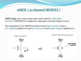
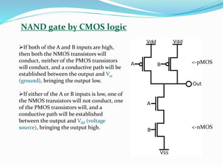
NMOS, PMOS, and CMOS logic gates are implemented using MOSFET transistors.
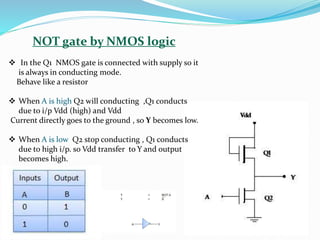
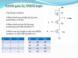
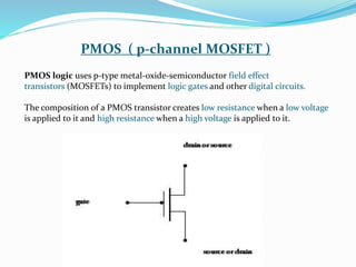
NMOS logic uses n-type MOSFETs that have high resistance with low voltage and low resistance with high voltage. PMOS logic uses p-type MOSFETs that have the opposite behavior.
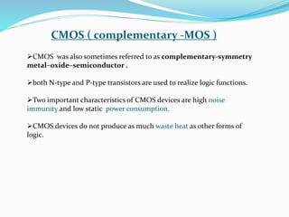
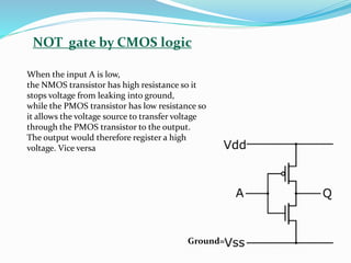
CMOS logic uses both n-type and p-type MOSFETs together to realize gates. When an input is low, the nMOS transistor stops current flow while the pMOS allows voltage through, giving a high output. This provides high noise immunity and low power consumption compared to NMOS and PMOS alone.