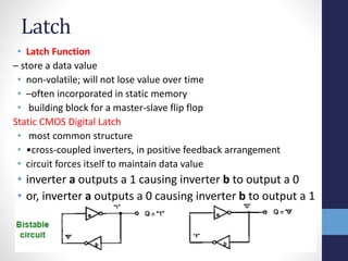
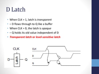
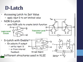
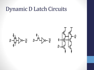
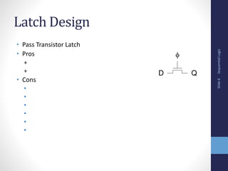
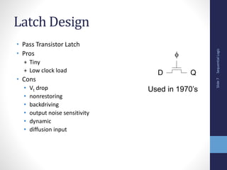
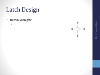
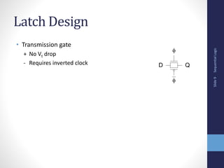
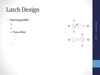
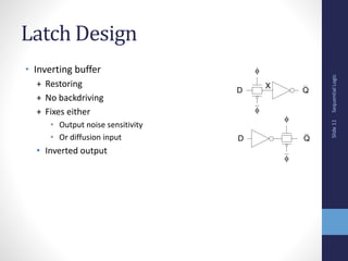
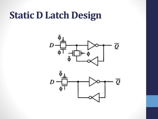
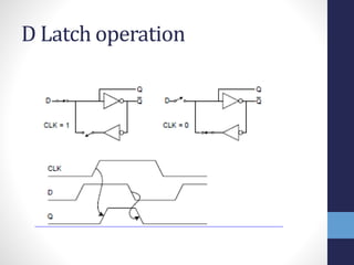
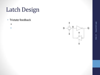
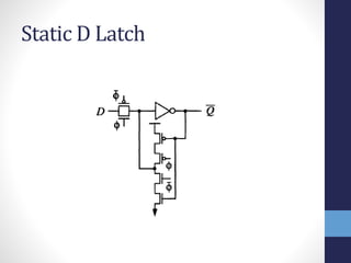
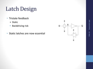
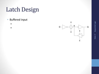
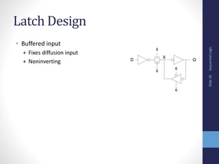
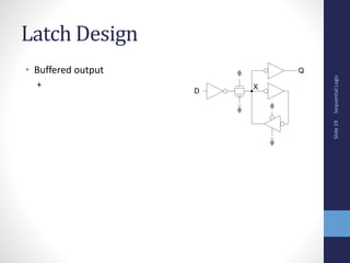
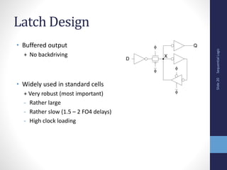
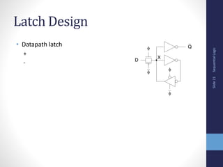
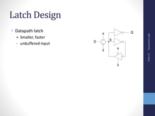
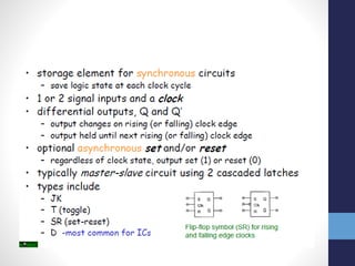
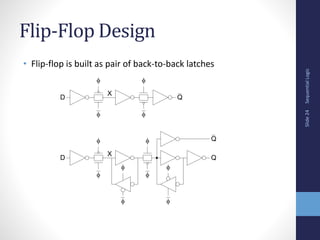
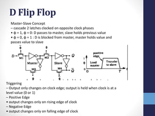
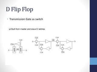
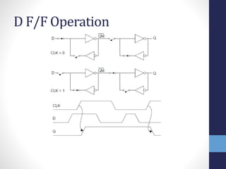
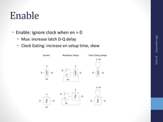
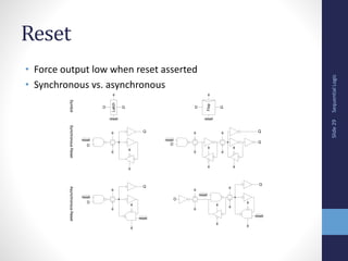
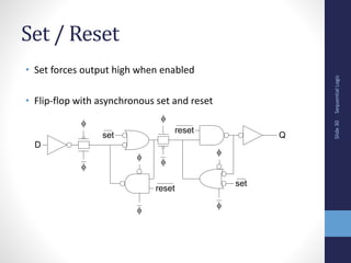
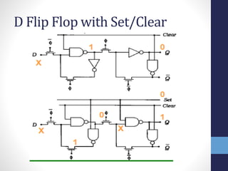
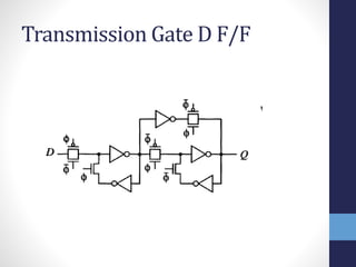
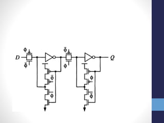
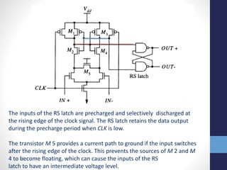
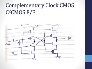
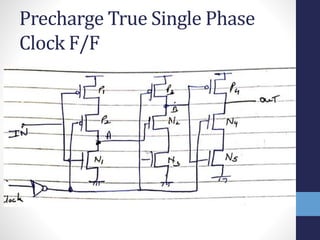
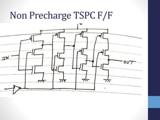
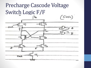
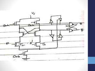
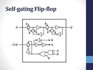
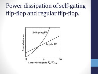
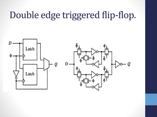
SlideShare a Scribd company logo
Latch & Flip-Flop
By:
Dr. Gargi Khanna
Assoc. Prof. ECE Deptt.
NIT Hamirpur
Latch
• Latch Function
– store a data value
• non-volatile; will not lose value over time
• –often incorporated in static memory
• building block for a master-slave flip flop
Static CMOS Digital Latch
• most common structure
• •cross-coupled inverters, in positive feedback arrangement
• circuit forces itself to maintain data value
• inverter a outputs a 1 causing inverter b to output a 0
• or, inverter a outputs a 0 causing inverter b to output a 1
D Latch
• When CLK = 1, latch is transparent
• – D flows through to Q like a buffer
• When CLK = 0, the latch is opaque
• – Q holds its old value independent of D
• Transparent latch or level-sensitive latch
D-Latch
Dynamic D Latch Circuits
Sequential
Logic
Slide
6
Latch Design
• Pass Transistor Latch
• Pros
+
+
• Cons
•
•
•
•
•
•
D Q

Sequential
Logic
Slide
7
Latch Design
• Pass Transistor Latch
• Pros
+ Tiny
+ Low clock load
• Cons
• Vt drop
• nonrestoring
• backdriving
• output noise sensitivity
• dynamic
• diffusion input
D Q

Used in 1970’s
Sequential
Logic
Slide
8
Latch Design
• Transmission gate
+
- D Q


Sequential
Logic
Slide
9
Latch Design
• Transmission gate
+ No Vt drop
- Requires inverted clock D Q


Sequential
Logic
Slide
10
Latch Design
• Inverting buffer
+
+
+ Fixes either
•
•
•
D


X
Q
D Q


Sequential
Logic
Slide
11
Latch Design
• Inverting buffer
+ Restoring
+ No backdriving
+ Fixes either
• Output noise sensitivity
• Or diffusion input
• Inverted output
D


X
Q
D Q


Static D Latch Design
D Latch operation
Sequential
Logic
Slide
14
Latch Design
• Tristate feedback
+
•




Q
D
X
Static D Latch
Sequential
Logic
Slide
16
Latch Design
• Tristate feedback
+ Static
• Backdriving risk
• Static latches are now essential




Q
D
X
Sequential
Logic
Slide
17
Latch Design
• Buffered input
+
+


Q
D
X


Sequential
Logic
Slide
18
Latch Design
• Buffered input
+ Fixes diffusion input
+ Noninverting


Q
D
X


Sequential
Logic
Slide
19
Latch Design
• Buffered output
+


Q
D
X


Sequential
Logic
Slide
20
Latch Design
• Buffered output
+ No backdriving
• Widely used in standard cells
+ Very robust (most important)
- Rather large
- Rather slow (1.5 – 2 FO4 delays)
- High clock loading


Q
D
X


Sequential
Logic
Slide
21
Latch Design
• Datapath latch
+
-




Q
D
X
Sequential
Logic
Slide
22
Latch Design
• Datapath latch
+ Smaller, faster
- unbuffered input




Q
D
X
Sequential
Logic
Slide
24
Flip-Flop Design
• Flip-flop is built as pair of back-to-back latches
D Q




X
D




X
Q
Q




D Flip Flop
Master-Slave Concept
– cascade 2 latches clocked on opposite clock phases
• φ = 1, φ = 0: D passes to master, slave holds previous value
• φ = 0, φ = 1 : D is blocked from master, master holds value and
passes value to slave
Triggering
– Output only changes on clock edge; output is held when clock is at a
level value (0 or 1)
– Positive Edge
• output changes only on rising edge of clock
– Negative Edge
• output changes only on falling edge of clock
D Flip Flop
• Transmission Gate as switch
D F/F Operation
Sequential
Logic
Slide
28
Enable
• Enable: ignore clock when en = 0
• Mux: increase latch D-Q delay
• Clock Gating: increase en setup time, skew
D Q
Latch
D Q
en
en


Latch
D
Q

0
1
en
Latch
D Q
 en
D
Q

0
1
en
D Q
 en
Flop
Flop
Flop
Symbol Multiplexer Design Clock Gating Design
Sequential
Logic
Slide
29
Reset
• Force output low when reset asserted
• Synchronous vs. asynchronous
D




Q
Q




reset
D






Q


D
reset


Q


D
reset
reset


reset
Synchronous
Reset
Asynchronous
Reset
Symbol
Flop
D Q
Latch
D Q
reset reset
 


Q
reset
Sequential
Logic
Slide
30
Set / Reset
• Set forces output high when enabled
• Flip-flop with asynchronous set and reset
D






Q


reset
set
reset
set
D Flip Flop with Set/Clear
Transmission Gate D F/F
The inputs of the RS latch are precharged and selectively discharged at
the rising edge of the clock signal. The RS latch retains the data output
during the precharge period when CLK is low.
The transistor M 5 provides a current path to ground if the input switches
after the rising edge of the clock. This prevents the sources of M 2 and M
4 to become floating, which can cause the inputs of the RS
latch to have an intermediate voltage level.
Complementary Clock CMOS
C2CMOS F/F
Precharge True Single Phase
Clock F/F
Non Precharge TSPC F/F
Precharge Cascode Voltage
Switch Logic F/F
Self-gating Flip-flop
Power dissipation of self-gating
flip-flop and regular flip-flop.
Double edge triggered flip-flop.
Power consumption of SETFF and
DETFF
Latch & Flip-Flop.pptx

More Related Content

What's hot

Clock Gating
Clock GatingClock Gating
Clock Gating
Mahesh Dananjaya
 
Vlsi interview questions compilation
Vlsi interview questions compilationVlsi interview questions compilation
Vlsi interview questions compilation
Rajesh M
 
Special technique in Low Power VLSI design
Special technique in Low Power VLSI designSpecial technique in Low Power VLSI design
Special technique in Low Power VLSI design
shrutishreya14
 
FPGA
FPGAFPGA
VLSI Design Sequential circuit design
VLSI Design Sequential circuit designVLSI Design Sequential circuit design
VLSI Design Sequential circuit design
tamil arasan
 
Multi mode multi corner (mmmc)
Multi mode multi corner (mmmc)Multi mode multi corner (mmmc)
Multi mode multi corner (mmmc)
shaik sharief
 
Combinational Logic Circuit
Combinational Logic CircuitCombinational Logic Circuit
Combinational Logic Circuit
GargiKhanna1
 
Sta by usha_mehta
Sta by usha_mehtaSta by usha_mehta
Sta by usha_mehta
Usha Mehta
 
Power dissipation cmos
Power dissipation cmosPower dissipation cmos
Power dissipation cmos
Rajesh Tiwary
 
Interconnect timing model
Interconnect  timing modelInterconnect  timing model
Interconnect timing model
Prachi Pandey
 
Timing analysis
Timing analysisTiming analysis
Timing analysis
Kunal Doshi
 
Reversible Logic Gate
Reversible Logic GateReversible Logic Gate
Reversible Logic Gate
Aneesh Raveendran
 
CMOS
CMOS CMOS
Power Gating
Power GatingPower Gating
Power Gating
Mahesh Dananjaya
 
Field Programmable Gate Array: Building Blocks and Interconnections
Field Programmable Gate Array: Building Blocks and InterconnectionsField Programmable Gate Array: Building Blocks and Interconnections
Field Programmable Gate Array: Building Blocks and Interconnections
Dr. Saravanakumar Umathurai
 
VLSI Power Reduction
VLSI Power ReductionVLSI Power Reduction
VLSI Power Reduction
Mahesh Dananjaya
 
Low Power VLSI Design
Low Power VLSI DesignLow Power VLSI Design
Low Power VLSI Design
Mahesh Dananjaya
 
Clock gating
Clock gatingClock gating
Clock gating
Mahi
 
digital logic_families
digital logic_familiesdigital logic_families
digital logic_families
Patel Jay
 

What's hot (20)

Clock Gating
Clock GatingClock Gating
Clock Gating
 
Vlsi interview questions compilation
Vlsi interview questions compilationVlsi interview questions compilation
Vlsi interview questions compilation
 
Special technique in Low Power VLSI design
Special technique in Low Power VLSI designSpecial technique in Low Power VLSI design
Special technique in Low Power VLSI design
 
FPGA
FPGAFPGA
FPGA
 
VLSI Design Sequential circuit design
VLSI Design Sequential circuit designVLSI Design Sequential circuit design
VLSI Design Sequential circuit design
 
Multi mode multi corner (mmmc)
Multi mode multi corner (mmmc)Multi mode multi corner (mmmc)
Multi mode multi corner (mmmc)
 
Analog vlsi
Analog vlsiAnalog vlsi
Analog vlsi
 
Combinational Logic Circuit
Combinational Logic CircuitCombinational Logic Circuit
Combinational Logic Circuit
 
Sta by usha_mehta
Sta by usha_mehtaSta by usha_mehta
Sta by usha_mehta
 
Power dissipation cmos
Power dissipation cmosPower dissipation cmos
Power dissipation cmos
 
Interconnect timing model
Interconnect  timing modelInterconnect  timing model
Interconnect timing model
 
Timing analysis
Timing analysisTiming analysis
Timing analysis
 
Reversible Logic Gate
Reversible Logic GateReversible Logic Gate
Reversible Logic Gate
 
CMOS
CMOS CMOS
CMOS
 
Power Gating
Power GatingPower Gating
Power Gating
 
Field Programmable Gate Array: Building Blocks and Interconnections
Field Programmable Gate Array: Building Blocks and InterconnectionsField Programmable Gate Array: Building Blocks and Interconnections
Field Programmable Gate Array: Building Blocks and Interconnections
 
VLSI Power Reduction
VLSI Power ReductionVLSI Power Reduction
VLSI Power Reduction
 
Low Power VLSI Design
Low Power VLSI DesignLow Power VLSI Design
Low Power VLSI Design
 
Clock gating
Clock gatingClock gating
Clock gating
 
digital logic_families
digital logic_familiesdigital logic_families
digital logic_families
 

Similar to Latch & Flip-Flop.pptx

Computer Organization1CS1400Feng JiangBoolean al.docx
Computer Organization1CS1400Feng JiangBoolean al.docxComputer Organization1CS1400Feng JiangBoolean al.docx
Computer Organization1CS1400Feng JiangBoolean al.docx
ladonnacamplin
 
FlipFlopsLatches off different inputs a and b
FlipFlopsLatches off different inputs a and bFlipFlopsLatches off different inputs a and b
FlipFlopsLatches off different inputs a and b
Meenakshi Munjal
 
FlipFlopsLatches1.ppt
FlipFlopsLatches1.pptFlipFlopsLatches1.ppt
FlipFlopsLatches1.ppt
manasSinghal11
 
FlipFlopsLatches1.ppt
FlipFlopsLatches1.pptFlipFlopsLatches1.ppt
FlipFlopsLatches1.ppt
diganta das
 
FlipFlopsLatches1.ppt
FlipFlopsLatches1.pptFlipFlopsLatches1.ppt
FlipFlopsLatches1.ppt
diganta das
 
FlipFlopsLatches1 (3).ppt
FlipFlopsLatches1 (3).pptFlipFlopsLatches1 (3).ppt
FlipFlopsLatches1 (3).ppt
SalmanHameed26
 
Ff 2
Ff 2Ff 2
Cse(b) g1 flipflop
Cse(b) g1 flipflopCse(b) g1 flipflop
Cse(b) g1 flipflop
KaranAgarwal71
 
D flip flop in Digital electronics
D flip flop in Digital electronicsD flip flop in Digital electronics
D flip flop in Digital electronics
Easy n Inspire L
 
Digital_Electronics_Module_4_Sequential_Circuits v0.6.pptx
Digital_Electronics_Module_4_Sequential_Circuits v0.6.pptxDigital_Electronics_Module_4_Sequential_Circuits v0.6.pptx
Digital_Electronics_Module_4_Sequential_Circuits v0.6.pptx
UtsavDas21
 
Flip flops
Flip flopsFlip flops
Flip flops
rameshthombre1
 
Sequntial logic design
Sequntial logic designSequntial logic design
Sequntial logic design
Pavan Mukku
 
latchesandflipflops.ppt
latchesandflipflops.pptlatchesandflipflops.ppt
latchesandflipflops.ppt
MuhammadSheraz836877
 
Latches and flip flops
Latches and flip flopsLatches and flip flops
Latches and flip flops
sheheryar ahmed
 
Lec14 Intro to Computer Engineering by Hsien-Hsin Sean Lee Georgia Tech -- Se...
Lec14 Intro to Computer Engineering by Hsien-Hsin Sean Lee Georgia Tech -- Se...Lec14 Intro to Computer Engineering by Hsien-Hsin Sean Lee Georgia Tech -- Se...
Lec14 Intro to Computer Engineering by Hsien-Hsin Sean Lee Georgia Tech -- Se...
Hsien-Hsin Sean Lee, Ph.D.
 
Sequential Logic Circuit
Sequential Logic CircuitSequential Logic Circuit
Sequential Logic Circuit
Yong Heui Cho
 
latchesflip-flop DLD
latchesflip-flop DLDlatchesflip-flop DLD
latchesflip-flop DLD
MuhammadSheraz836877
 
Latches & flip flop
Latches & flip flopLatches & flip flop
Latches & flip flop
Nousheen Arshad
 
Lecture22
Lecture22Lecture22
Lecture22
Dharmesh Goyal
 

Similar to Latch & Flip-Flop.pptx (20)

Computer Organization1CS1400Feng JiangBoolean al.docx
Computer Organization1CS1400Feng JiangBoolean al.docxComputer Organization1CS1400Feng JiangBoolean al.docx
Computer Organization1CS1400Feng JiangBoolean al.docx
 
FlipFlopsLatches off different inputs a and b
FlipFlopsLatches off different inputs a and bFlipFlopsLatches off different inputs a and b
FlipFlopsLatches off different inputs a and b
 
FlipFlopsLatches1.ppt
FlipFlopsLatches1.pptFlipFlopsLatches1.ppt
FlipFlopsLatches1.ppt
 
FlipFlopsLatches1.ppt
FlipFlopsLatches1.pptFlipFlopsLatches1.ppt
FlipFlopsLatches1.ppt
 
FlipFlopsLatches1.ppt
FlipFlopsLatches1.pptFlipFlopsLatches1.ppt
FlipFlopsLatches1.ppt
 
FlipFlopsLatches1 (3).ppt
FlipFlopsLatches1 (3).pptFlipFlopsLatches1 (3).ppt
FlipFlopsLatches1 (3).ppt
 
Ff 2
Ff 2Ff 2
Ff 2
 
Flip flop
Flip flopFlip flop
Flip flop
 
Cse(b) g1 flipflop
Cse(b) g1 flipflopCse(b) g1 flipflop
Cse(b) g1 flipflop
 
D flip flop in Digital electronics
D flip flop in Digital electronicsD flip flop in Digital electronics
D flip flop in Digital electronics
 
Digital_Electronics_Module_4_Sequential_Circuits v0.6.pptx
Digital_Electronics_Module_4_Sequential_Circuits v0.6.pptxDigital_Electronics_Module_4_Sequential_Circuits v0.6.pptx
Digital_Electronics_Module_4_Sequential_Circuits v0.6.pptx
 
Flip flops
Flip flopsFlip flops
Flip flops
 
Sequntial logic design
Sequntial logic designSequntial logic design
Sequntial logic design
 
latchesandflipflops.ppt
latchesandflipflops.pptlatchesandflipflops.ppt
latchesandflipflops.ppt
 
Latches and flip flops
Latches and flip flopsLatches and flip flops
Latches and flip flops
 
Lec14 Intro to Computer Engineering by Hsien-Hsin Sean Lee Georgia Tech -- Se...
Lec14 Intro to Computer Engineering by Hsien-Hsin Sean Lee Georgia Tech -- Se...Lec14 Intro to Computer Engineering by Hsien-Hsin Sean Lee Georgia Tech -- Se...
Lec14 Intro to Computer Engineering by Hsien-Hsin Sean Lee Georgia Tech -- Se...
 
Sequential Logic Circuit
Sequential Logic CircuitSequential Logic Circuit
Sequential Logic Circuit
 
latchesflip-flop DLD
latchesflip-flop DLDlatchesflip-flop DLD
latchesflip-flop DLD
 
Latches & flip flop
Latches & flip flopLatches & flip flop
Latches & flip flop
 
Lecture22
Lecture22Lecture22
Lecture22
 

More from GargiKhanna1

MOS logic family
MOS logic familyMOS logic family
MOS logic family
GargiKhanna1
 
Digital Counter Design
 Digital Counter Design Digital Counter Design
Digital Counter Design
GargiKhanna1
 
Multiplexers and Demultiplexers
Multiplexers and DemultiplexersMultiplexers and Demultiplexers
Multiplexers and Demultiplexers
GargiKhanna1
 
Karnaugh Map
Karnaugh MapKarnaugh Map
Karnaugh Map
GargiKhanna1
 
Error detection and correction codes
Error detection and correction codesError detection and correction codes
Error detection and correction codes
GargiKhanna1
 
Number system
Number system Number system
Number system
GargiKhanna1
 
Boolean Function SOP & POS
Boolean Function SOP &  POSBoolean Function SOP &  POS
Boolean Function SOP & POS
GargiKhanna1
 
Logic gate
Logic gateLogic gate
Logic gate
GargiKhanna1
 
Logic Gates
Logic GatesLogic Gates
Logic Gates
GargiKhanna1
 
Binary codes
Binary codesBinary codes
Binary codes
GargiKhanna1
 
Binary Arithmetic
Binary ArithmeticBinary Arithmetic
Binary Arithmetic
GargiKhanna1
 

More from GargiKhanna1 (11)

MOS logic family
MOS logic familyMOS logic family
MOS logic family
 
Digital Counter Design
 Digital Counter Design Digital Counter Design
Digital Counter Design
 
Multiplexers and Demultiplexers
Multiplexers and DemultiplexersMultiplexers and Demultiplexers
Multiplexers and Demultiplexers
 
Karnaugh Map
Karnaugh MapKarnaugh Map
Karnaugh Map
 
Error detection and correction codes
Error detection and correction codesError detection and correction codes
Error detection and correction codes
 
Number system
Number system Number system
Number system
 
Boolean Function SOP & POS
Boolean Function SOP &  POSBoolean Function SOP &  POS
Boolean Function SOP & POS
 
Logic gate
Logic gateLogic gate
Logic gate
 
Logic Gates
Logic GatesLogic Gates
Logic Gates
 
Binary codes
Binary codesBinary codes
Binary codes
 
Binary Arithmetic
Binary ArithmeticBinary Arithmetic
Binary Arithmetic
 

Recently uploaded

block diagram and signal flow graph representation
block diagram and signal flow graph representationblock diagram and signal flow graph representation
block diagram and signal flow graph representation
Divya Somashekar
 
Industrial Training at Shahjalal Fertilizer Company Limited (SFCL)
Industrial Training at Shahjalal Fertilizer Company Limited (SFCL)Industrial Training at Shahjalal Fertilizer Company Limited (SFCL)
Industrial Training at Shahjalal Fertilizer Company Limited (SFCL)
MdTanvirMahtab2
 
Water Industry Process Automation and Control Monthly - May 2024.pdf
Water Industry Process Automation and Control Monthly - May 2024.pdfWater Industry Process Automation and Control Monthly - May 2024.pdf
Water Industry Process Automation and Control Monthly - May 2024.pdf
Water Industry Process Automation & Control
 
J.Yang, ICLR 2024, MLILAB, KAIST AI.pdf
J.Yang,  ICLR 2024, MLILAB, KAIST AI.pdfJ.Yang,  ICLR 2024, MLILAB, KAIST AI.pdf
J.Yang, ICLR 2024, MLILAB, KAIST AI.pdf
MLILAB
 
CFD Simulation of By-pass Flow in a HRSG module by R&R Consult.pptx
CFD Simulation of By-pass Flow in a HRSG module by R&R Consult.pptxCFD Simulation of By-pass Flow in a HRSG module by R&R Consult.pptx
CFD Simulation of By-pass Flow in a HRSG module by R&R Consult.pptx
R&R Consult
 
HYDROPOWER - Hydroelectric power generation
HYDROPOWER - Hydroelectric power generationHYDROPOWER - Hydroelectric power generation
HYDROPOWER - Hydroelectric power generation
Robbie Edward Sayers
 
Nuclear Power Economics and Structuring 2024
Nuclear Power Economics and Structuring 2024Nuclear Power Economics and Structuring 2024
Nuclear Power Economics and Structuring 2024
Massimo Talia
 
The Benefits and Techniques of Trenchless Pipe Repair.pdf
The Benefits and Techniques of Trenchless Pipe Repair.pdfThe Benefits and Techniques of Trenchless Pipe Repair.pdf
The Benefits and Techniques of Trenchless Pipe Repair.pdf
Pipe Restoration Solutions
 
AP LAB PPT.pdf ap lab ppt no title specific
AP LAB PPT.pdf ap lab ppt no title specificAP LAB PPT.pdf ap lab ppt no title specific
AP LAB PPT.pdf ap lab ppt no title specific
BrazilAccount1
 
Student information management system project report ii.pdf
Student information management system project report ii.pdfStudent information management system project report ii.pdf
Student information management system project report ii.pdf
Kamal Acharya
 
Standard Reomte Control Interface - Neometrix
Standard Reomte Control Interface - NeometrixStandard Reomte Control Interface - Neometrix
Standard Reomte Control Interface - Neometrix
Neometrix_Engineering_Pvt_Ltd
 
English lab ppt no titlespecENG PPTt.pdf
English lab ppt no titlespecENG PPTt.pdfEnglish lab ppt no titlespecENG PPTt.pdf
English lab ppt no titlespecENG PPTt.pdf
BrazilAccount1
 
一比一原版(SFU毕业证)西蒙菲莎大学毕业证成绩单如何办理
一比一原版(SFU毕业证)西蒙菲莎大学毕业证成绩单如何办理一比一原版(SFU毕业证)西蒙菲莎大学毕业证成绩单如何办理
一比一原版(SFU毕业证)西蒙菲莎大学毕业证成绩单如何办理
bakpo1
 
ethical hacking-mobile hacking methods.ppt
ethical hacking-mobile hacking methods.pptethical hacking-mobile hacking methods.ppt
ethical hacking-mobile hacking methods.ppt
Jayaprasanna4
 
ASME IX(9) 2007 Full Version .pdf
ASME IX(9)  2007 Full Version       .pdfASME IX(9)  2007 Full Version       .pdf
ASME IX(9) 2007 Full Version .pdf
AhmedHussein950959
 
ML for identifying fraud using open blockchain data.pptx
ML for identifying fraud using open blockchain data.pptxML for identifying fraud using open blockchain data.pptx
ML for identifying fraud using open blockchain data.pptx
Vijay Dialani, PhD
 
Hybrid optimization of pumped hydro system and solar- Engr. Abdul-Azeez.pdf
Hybrid optimization of pumped hydro system and solar- Engr. Abdul-Azeez.pdfHybrid optimization of pumped hydro system and solar- Engr. Abdul-Azeez.pdf
Hybrid optimization of pumped hydro system and solar- Engr. Abdul-Azeez.pdf
fxintegritypublishin
 
road safety engineering r s e unit 3.pdf
road safety engineering  r s e unit 3.pdfroad safety engineering  r s e unit 3.pdf
road safety engineering r s e unit 3.pdf
VENKATESHvenky89705
 
weather web application report.pdf
weather web application report.pdfweather web application report.pdf
weather web application report.pdf
Pratik Pawar
 
Runway Orientation Based on the Wind Rose Diagram.pptx
Runway Orientation Based on the Wind Rose Diagram.pptxRunway Orientation Based on the Wind Rose Diagram.pptx
Runway Orientation Based on the Wind Rose Diagram.pptx
SupreethSP4
 

Recently uploaded (20)

block diagram and signal flow graph representation
block diagram and signal flow graph representationblock diagram and signal flow graph representation
block diagram and signal flow graph representation
 
Industrial Training at Shahjalal Fertilizer Company Limited (SFCL)
Industrial Training at Shahjalal Fertilizer Company Limited (SFCL)Industrial Training at Shahjalal Fertilizer Company Limited (SFCL)
Industrial Training at Shahjalal Fertilizer Company Limited (SFCL)
 
Water Industry Process Automation and Control Monthly - May 2024.pdf
Water Industry Process Automation and Control Monthly - May 2024.pdfWater Industry Process Automation and Control Monthly - May 2024.pdf
Water Industry Process Automation and Control Monthly - May 2024.pdf
 
J.Yang, ICLR 2024, MLILAB, KAIST AI.pdf
J.Yang,  ICLR 2024, MLILAB, KAIST AI.pdfJ.Yang,  ICLR 2024, MLILAB, KAIST AI.pdf
J.Yang, ICLR 2024, MLILAB, KAIST AI.pdf
 
CFD Simulation of By-pass Flow in a HRSG module by R&R Consult.pptx
CFD Simulation of By-pass Flow in a HRSG module by R&R Consult.pptxCFD Simulation of By-pass Flow in a HRSG module by R&R Consult.pptx
CFD Simulation of By-pass Flow in a HRSG module by R&R Consult.pptx
 
HYDROPOWER - Hydroelectric power generation
HYDROPOWER - Hydroelectric power generationHYDROPOWER - Hydroelectric power generation
HYDROPOWER - Hydroelectric power generation
 
Nuclear Power Economics and Structuring 2024
Nuclear Power Economics and Structuring 2024Nuclear Power Economics and Structuring 2024
Nuclear Power Economics and Structuring 2024
 
The Benefits and Techniques of Trenchless Pipe Repair.pdf
The Benefits and Techniques of Trenchless Pipe Repair.pdfThe Benefits and Techniques of Trenchless Pipe Repair.pdf
The Benefits and Techniques of Trenchless Pipe Repair.pdf
 
AP LAB PPT.pdf ap lab ppt no title specific
AP LAB PPT.pdf ap lab ppt no title specificAP LAB PPT.pdf ap lab ppt no title specific
AP LAB PPT.pdf ap lab ppt no title specific
 
Student information management system project report ii.pdf
Student information management system project report ii.pdfStudent information management system project report ii.pdf
Student information management system project report ii.pdf
 
Standard Reomte Control Interface - Neometrix
Standard Reomte Control Interface - NeometrixStandard Reomte Control Interface - Neometrix
Standard Reomte Control Interface - Neometrix
 
English lab ppt no titlespecENG PPTt.pdf
English lab ppt no titlespecENG PPTt.pdfEnglish lab ppt no titlespecENG PPTt.pdf
English lab ppt no titlespecENG PPTt.pdf
 
一比一原版(SFU毕业证)西蒙菲莎大学毕业证成绩单如何办理
一比一原版(SFU毕业证)西蒙菲莎大学毕业证成绩单如何办理一比一原版(SFU毕业证)西蒙菲莎大学毕业证成绩单如何办理
一比一原版(SFU毕业证)西蒙菲莎大学毕业证成绩单如何办理
 
ethical hacking-mobile hacking methods.ppt
ethical hacking-mobile hacking methods.pptethical hacking-mobile hacking methods.ppt
ethical hacking-mobile hacking methods.ppt
 
ASME IX(9) 2007 Full Version .pdf
ASME IX(9)  2007 Full Version       .pdfASME IX(9)  2007 Full Version       .pdf
ASME IX(9) 2007 Full Version .pdf
 
ML for identifying fraud using open blockchain data.pptx
ML for identifying fraud using open blockchain data.pptxML for identifying fraud using open blockchain data.pptx
ML for identifying fraud using open blockchain data.pptx
 
Hybrid optimization of pumped hydro system and solar- Engr. Abdul-Azeez.pdf
Hybrid optimization of pumped hydro system and solar- Engr. Abdul-Azeez.pdfHybrid optimization of pumped hydro system and solar- Engr. Abdul-Azeez.pdf
Hybrid optimization of pumped hydro system and solar- Engr. Abdul-Azeez.pdf
 
road safety engineering r s e unit 3.pdf
road safety engineering  r s e unit 3.pdfroad safety engineering  r s e unit 3.pdf
road safety engineering r s e unit 3.pdf
 
weather web application report.pdf
weather web application report.pdfweather web application report.pdf
weather web application report.pdf
 
Runway Orientation Based on the Wind Rose Diagram.pptx
Runway Orientation Based on the Wind Rose Diagram.pptxRunway Orientation Based on the Wind Rose Diagram.pptx
Runway Orientation Based on the Wind Rose Diagram.pptx
 

Latch & Flip-Flop.pptx

Editor's Notes

  1. This circuit was reportedly used in a RISC microprocessor [4.14]. The flip-flop contains a simple differential feedback circuit that drives an RS latch. The transistors M I' M 2' M 3' M 4 form a pair of cross coupled feedback inverters. The inputs of the RS latch are precharged and selectively discharged at the rising edge of the clock signal. The RS latch retains the data output during the precharge period when CLK is low. The transistor M 5 provides a current path to ground if the input switches after the rising edge of the clock. This prevents the sources of M 2 and M 4 to become floating, which can cause the inputs of the RS latch to have an intermediate voltage level. Although only three transistors are connected to the single phase clock signal, one of the nodes at the inputs of the RS latch is always charged and discharged during evaluation. Note that the full CMOS implementation does not consume static current when the clock is stopped.