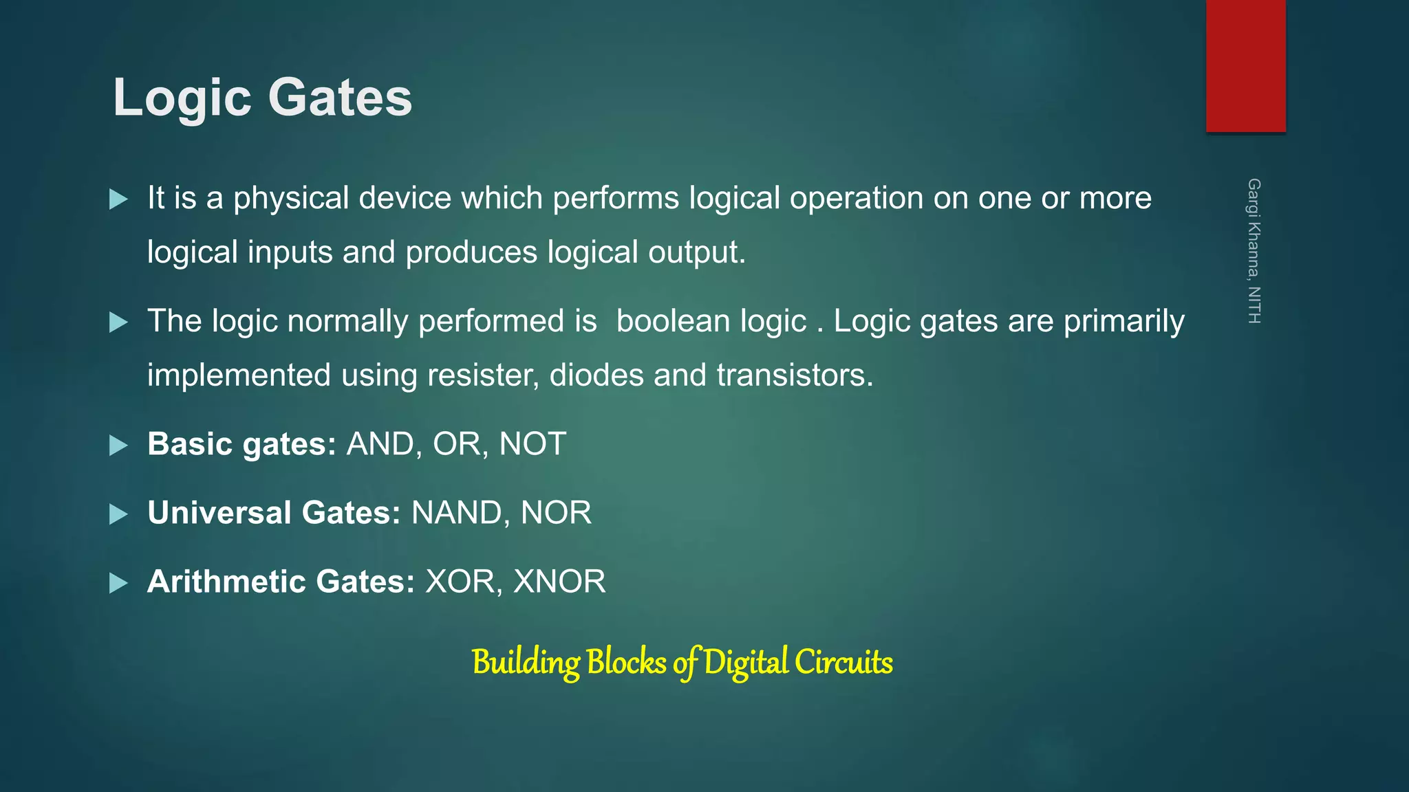
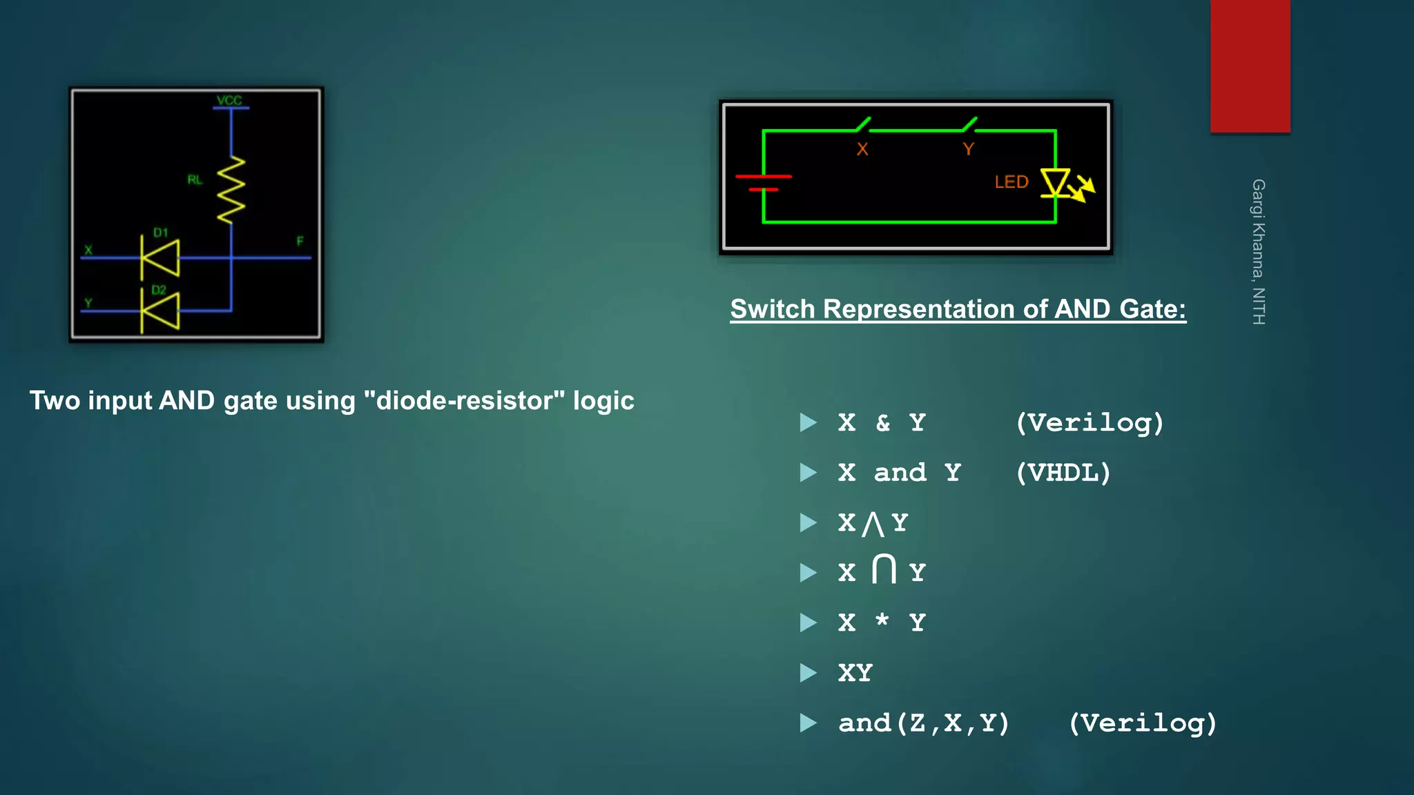
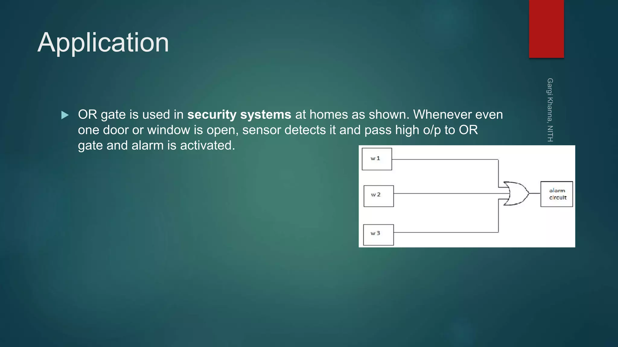
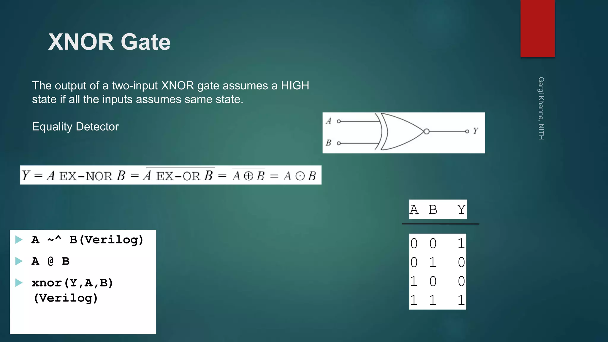
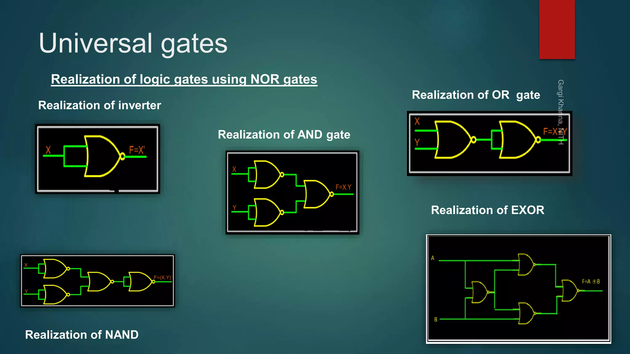
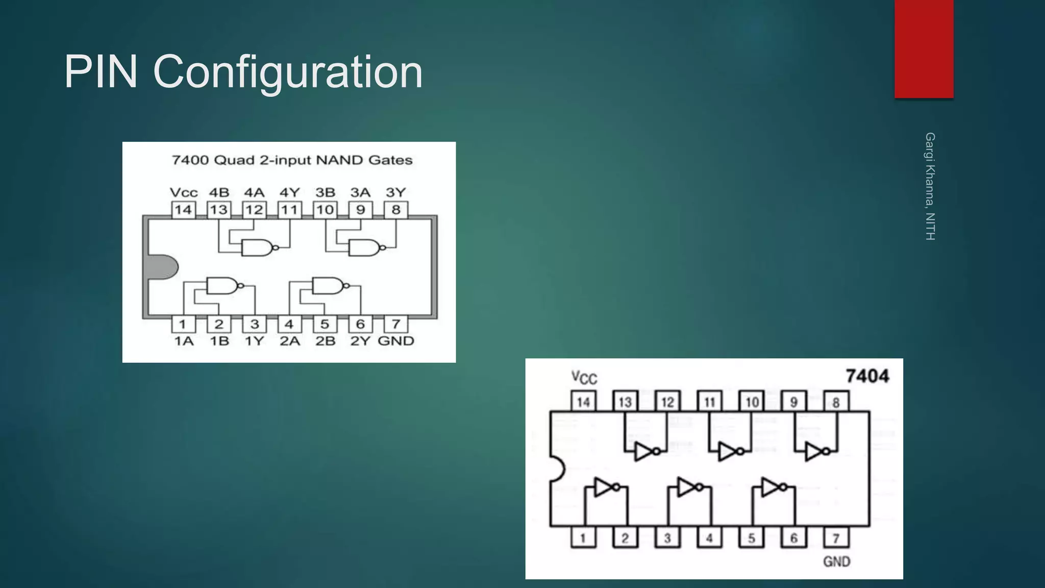
Dr. (Mrs.) Gargi Khanna
Associate Professor
Electronics & Communication Engineering Department
National Institute of Technology, Hamirpur
Digital Electronics & Logic Design
Logic Gates
Digital Signal
 A digital signal has two discrete levels or values.
 These levels can be represented using the terms LOW and HIGH.
 Two discrete signal levels HIGH and LOW can also be represented by
the binary bit 1 and 0 respectively.
Logic Gates
 It is a physical device which performs logical operation on one or more
logical inputs and produces logical output.
 The logic normally performed is boolean logic . Logic gates are primarily
implemented using resister, diodes and transistors.
 Basic gates: AND, OR, NOT
 Universal Gates: NAND, NOR
 Arithmetic Gates: XOR, XNOR
Building Blocks of Digital Circuits
Characterization of Gate
 Truth table is a table that describes the behaviour of a logic gate or any
combination of logic gates. It lists the value of the output for every possible
combination of the inputs.
 Boolean Equation
 Symbol
NOT Gate (Inverter)
 The NOT gate performs the logical function called inversion or complementation.
 The purpose of this gate is to convert one logic level into the opposite logic level.
 It has one input and one output. When a HIGH level is applied to an inverter, a LOW level
appears on its output and vice versa.
NOT gate using "transistor-resistor" logic
APPLICATIONS:
Figure shows the circuit for producing 1’s compliment of an 4 bit binary number.the bits of binary numbers are applied to inverter inputs and 1’s compliment of the numbers is obtained at output
Switching Representation of NOT gate
1 1 0 1
0 0 1 0
Application
1’s compliment
 Y = ~X
(Verilog)
 Y = not X (VHDL)
 Y = X’
 not(Y,X) (Verilog)
AND Gate
 The output of AND gate is HIGH only when all its inputs are HIGH (i.e. even if one
input is LOW, Output will be LOW).
 Logical Multiplication
 It has n input (n >= 2) and one output.
X Y Z F=X.Y.Z
0 0 0 0
0 0 1 0
0 1 0 0
0 1 1 0
1 0 0 0
1 0 1 0
1 1 0 0
1 1 1 1
(n = 2) (n = 3)
Two input AND gate using "diode-resistor" logic
Switch Representation of AND Gate:
 X & Y (Verilog)
 X and Y (VHDL)
 X Y
 X Y
 X * Y
 XY
 and(Z,X,Y) (Verilog)
U
V
APPLICATIONS of AND :
1. A seat belt alarm system
The AND gate as an enable/inhibit Device
3. Operating the locker in the bank
2.
OR Gate
 The OR gate has two or more inputs and single output.
 The output of OR gate is HIGH when any one of its inputs are HIGH
X Y Z F=X+Y+Z
0 0 0 0
0 0 1 1
0 1 0 1
0 1 1 1
1 0 0 1
1 0 1 1
1 1 0 1
1 1 1 1
Two input OR gate using "diode-resistor" logic
Switch Representation of OR Gate
 X | Y (Verilog)
 X or Y (VHDL)
 X + Y (textbook)
 X V Y
 X U Y
 or(Z,X,Y) (Verilog)
Application
 OR gate is used in security systems at homes as shown. Whenever even
one door or window is open, sensor detects it and pass high o/p to OR
gate and alarm is activated.
NAND Gate
 It has two or more inputs and only one output.
 The output of NAND gate is HIGH when any one of its input is LOW
 NAND gate is a cascade of AND gate and NOT gate.
NOR Gate
 It has two or more inputs and only one output.
 The output of NOR gate is HIGH when any all its inputs are LOW
XOR Gate
 The output of a two-input XOR gate assumes a
HIGH state if one and only one input assumes a
HIGH state.
 This is equivalent to saying that the output is
HIGH if either input X or input Y is HIGH
exclusively, and LOW when both are 1 or 0
simultaneously.
F= X.Y' + X'.Y
 X ^ Y (Verilog)
 X @ Y
 xor(Z,X,Y)
(Verilog)
X Y F
0 0 0
0 1 1
1 0 1
1 1 0
X
Y
Z
XNOR Gate
The output of a two-input XNOR gate assumes a HIGH
state if all the inputs assumes same state.
Equality Detector
 A ~^ B(Verilog)
 A @ B
 xnor(Y,A,B)
(Verilog)
A B Y
0 0 1
0 1 0
1 0 0
1 1 1
Universal gates
Realization of logic gates using NAND gates
Realization of inverter Realization of AND gate
Realization of OR gate
Realization of EXOR gate
Realization of EXNOR gate
Universal gates
Realization of logic gates using NOR gates
Realization of inverter
Realization of AND gate
Realization of OR gate
Realization of NAND
Realization of EXOR
IC Description
PIN Configuration
IC7432 IC7402
IC7486IC7410
Happy Learning

Logic Gates

  • 1.
    Dr. (Mrs.) GargiKhanna Associate Professor Electronics & Communication Engineering Department National Institute of Technology, Hamirpur Digital Electronics & Logic Design Logic Gates
  • 2.
    Digital Signal  Adigital signal has two discrete levels or values.  These levels can be represented using the terms LOW and HIGH.  Two discrete signal levels HIGH and LOW can also be represented by the binary bit 1 and 0 respectively.
  • 3.
    Logic Gates  Itis a physical device which performs logical operation on one or more logical inputs and produces logical output.  The logic normally performed is boolean logic . Logic gates are primarily implemented using resister, diodes and transistors.  Basic gates: AND, OR, NOT  Universal Gates: NAND, NOR  Arithmetic Gates: XOR, XNOR Building Blocks of Digital Circuits
  • 4.
    Characterization of Gate Truth table is a table that describes the behaviour of a logic gate or any combination of logic gates. It lists the value of the output for every possible combination of the inputs.  Boolean Equation  Symbol
  • 5.
    NOT Gate (Inverter) The NOT gate performs the logical function called inversion or complementation.  The purpose of this gate is to convert one logic level into the opposite logic level.  It has one input and one output. When a HIGH level is applied to an inverter, a LOW level appears on its output and vice versa.
  • 6.
    NOT gate using"transistor-resistor" logic APPLICATIONS: Figure shows the circuit for producing 1’s compliment of an 4 bit binary number.the bits of binary numbers are applied to inverter inputs and 1’s compliment of the numbers is obtained at output Switching Representation of NOT gate 1 1 0 1 0 0 1 0 Application 1’s compliment  Y = ~X (Verilog)  Y = not X (VHDL)  Y = X’  not(Y,X) (Verilog)
  • 7.
    AND Gate  Theoutput of AND gate is HIGH only when all its inputs are HIGH (i.e. even if one input is LOW, Output will be LOW).  Logical Multiplication  It has n input (n >= 2) and one output. X Y Z F=X.Y.Z 0 0 0 0 0 0 1 0 0 1 0 0 0 1 1 0 1 0 0 0 1 0 1 0 1 1 0 0 1 1 1 1 (n = 2) (n = 3)
  • 8.
    Two input ANDgate using "diode-resistor" logic Switch Representation of AND Gate:  X & Y (Verilog)  X and Y (VHDL)  X Y  X Y  X * Y  XY  and(Z,X,Y) (Verilog) U V
  • 9.
    APPLICATIONS of AND: 1. A seat belt alarm system The AND gate as an enable/inhibit Device 3. Operating the locker in the bank 2.
  • 10.
    OR Gate  TheOR gate has two or more inputs and single output.  The output of OR gate is HIGH when any one of its inputs are HIGH X Y Z F=X+Y+Z 0 0 0 0 0 0 1 1 0 1 0 1 0 1 1 1 1 0 0 1 1 0 1 1 1 1 0 1 1 1 1 1
  • 11.
    Two input ORgate using "diode-resistor" logic Switch Representation of OR Gate  X | Y (Verilog)  X or Y (VHDL)  X + Y (textbook)  X V Y  X U Y  or(Z,X,Y) (Verilog)
  • 12.
    Application  OR gateis used in security systems at homes as shown. Whenever even one door or window is open, sensor detects it and pass high o/p to OR gate and alarm is activated.
  • 13.
    NAND Gate  Ithas two or more inputs and only one output.  The output of NAND gate is HIGH when any one of its input is LOW  NAND gate is a cascade of AND gate and NOT gate.
  • 14.
    NOR Gate  Ithas two or more inputs and only one output.  The output of NOR gate is HIGH when any all its inputs are LOW
  • 15.
    XOR Gate  Theoutput of a two-input XOR gate assumes a HIGH state if one and only one input assumes a HIGH state.  This is equivalent to saying that the output is HIGH if either input X or input Y is HIGH exclusively, and LOW when both are 1 or 0 simultaneously. F= X.Y' + X'.Y  X ^ Y (Verilog)  X @ Y  xor(Z,X,Y) (Verilog) X Y F 0 0 0 0 1 1 1 0 1 1 1 0
  • 16.
  • 17.
    XNOR Gate The outputof a two-input XNOR gate assumes a HIGH state if all the inputs assumes same state. Equality Detector  A ~^ B(Verilog)  A @ B  xnor(Y,A,B) (Verilog) A B Y 0 0 1 0 1 0 1 0 0 1 1 1
  • 18.
    Universal gates Realization oflogic gates using NAND gates Realization of inverter Realization of AND gate Realization of OR gate Realization of EXOR gate Realization of EXNOR gate
  • 19.
    Universal gates Realization oflogic gates using NOR gates Realization of inverter Realization of AND gate Realization of OR gate Realization of NAND Realization of EXOR
  • 20.
  • 21.
  • 22.
  • 23.
  • 24.