Download to read offline

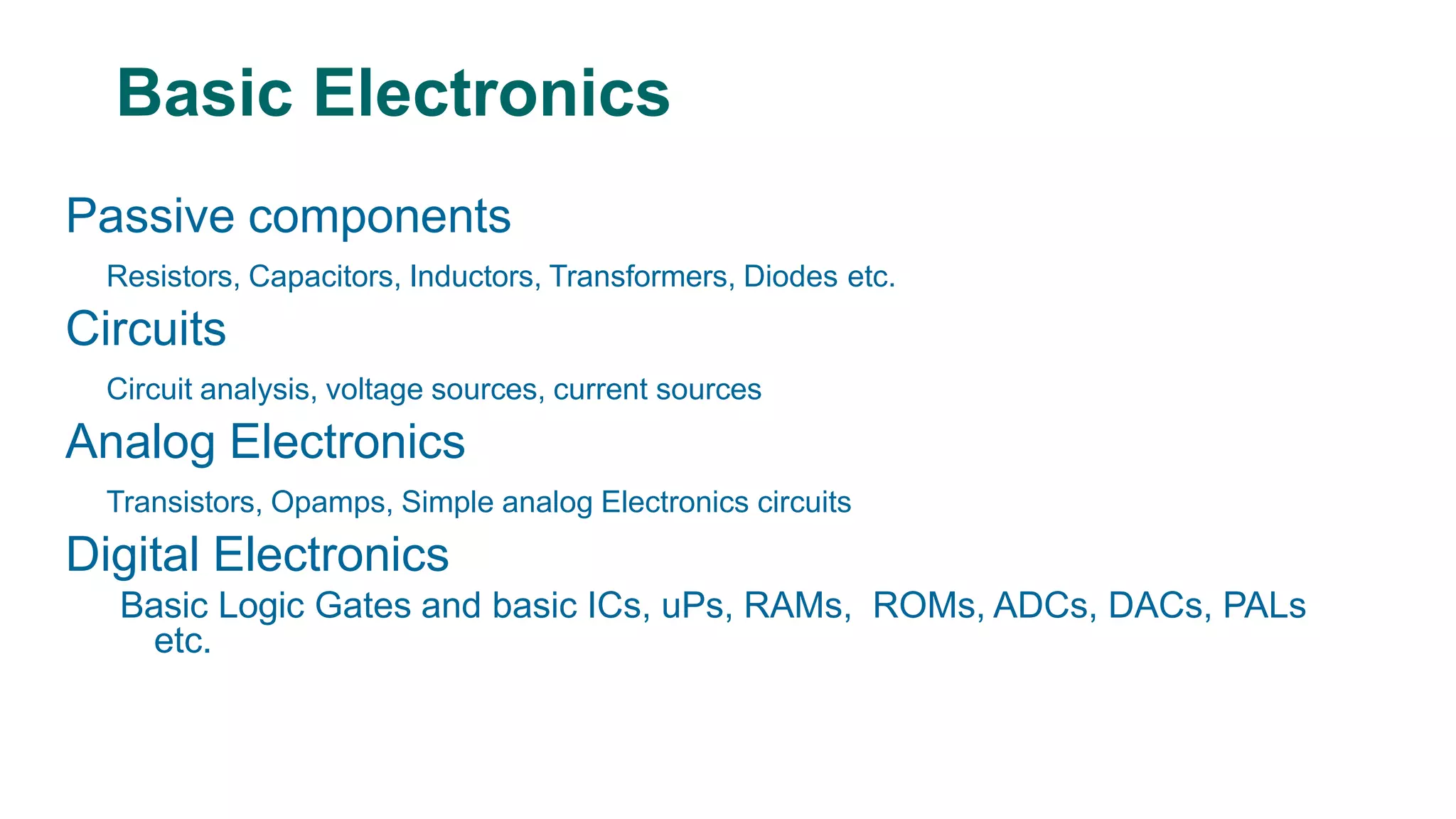
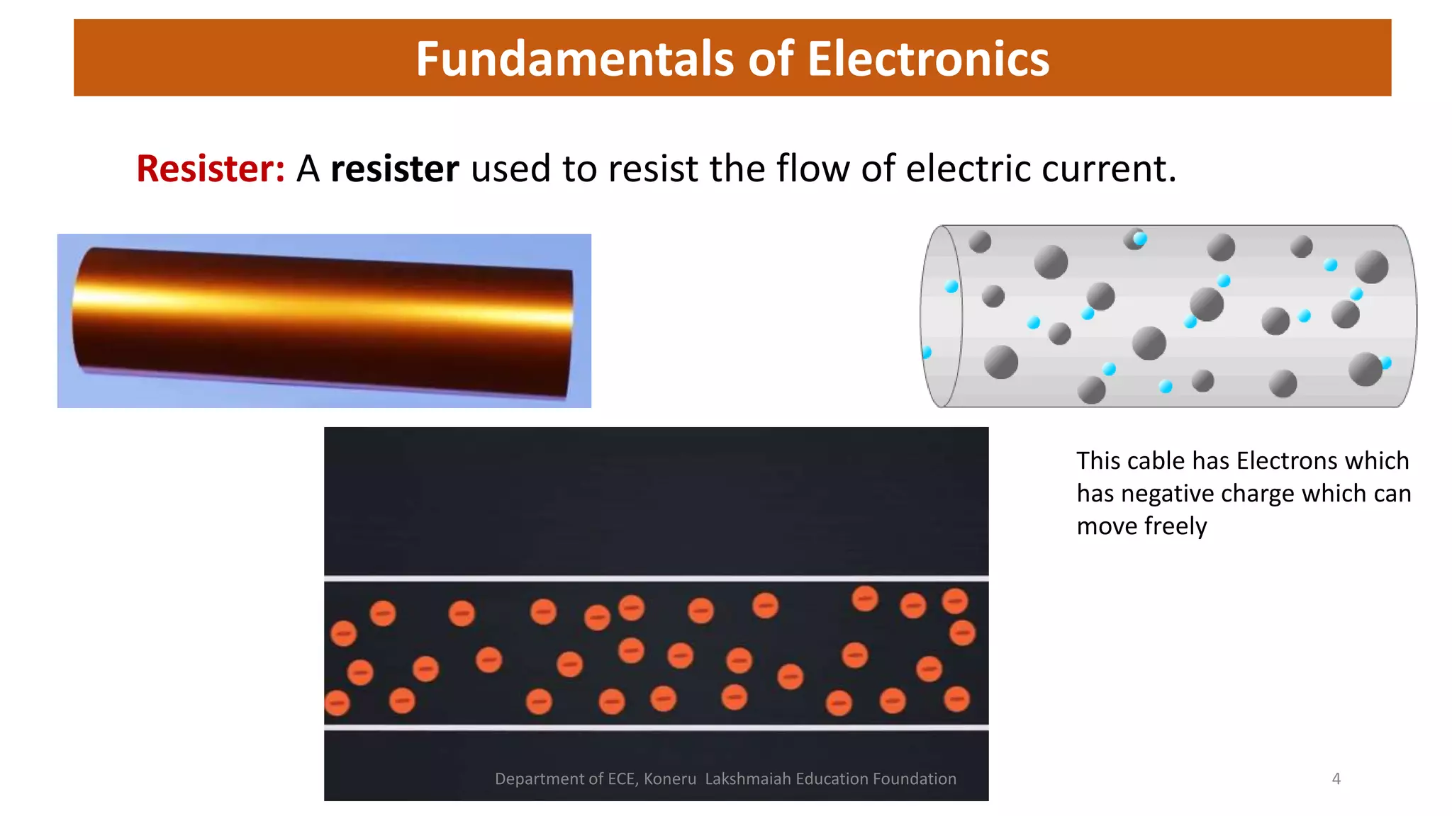
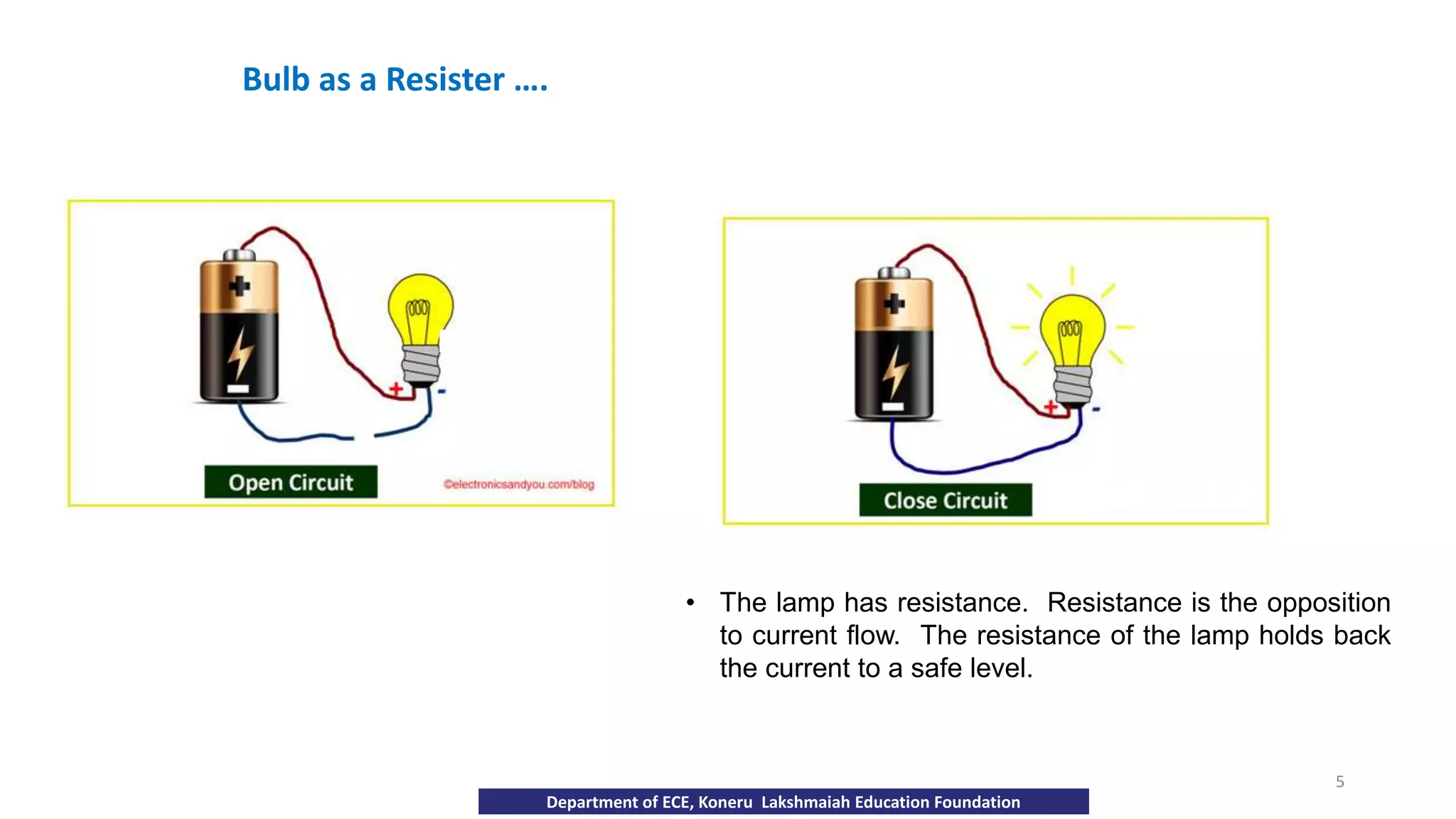
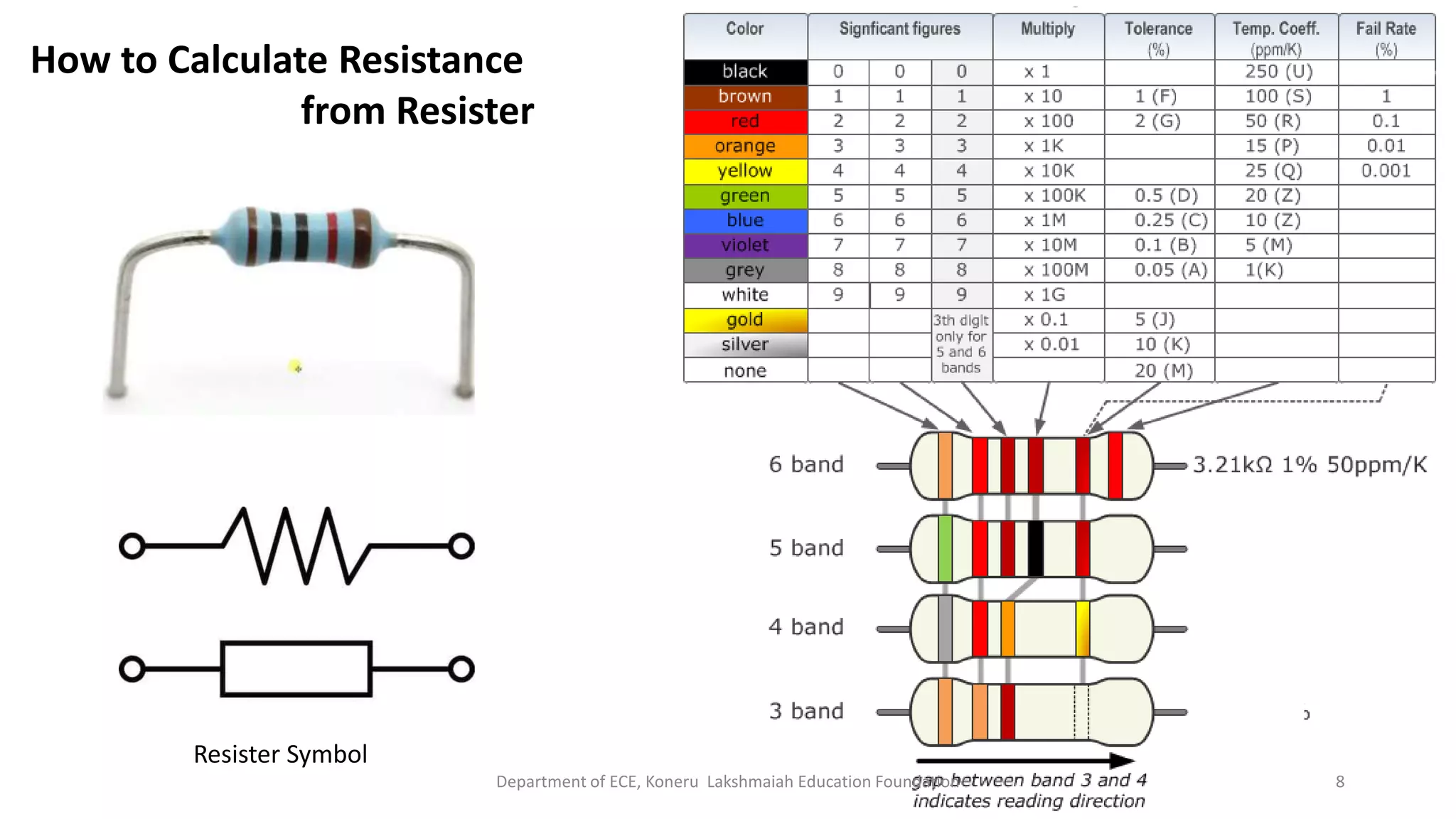
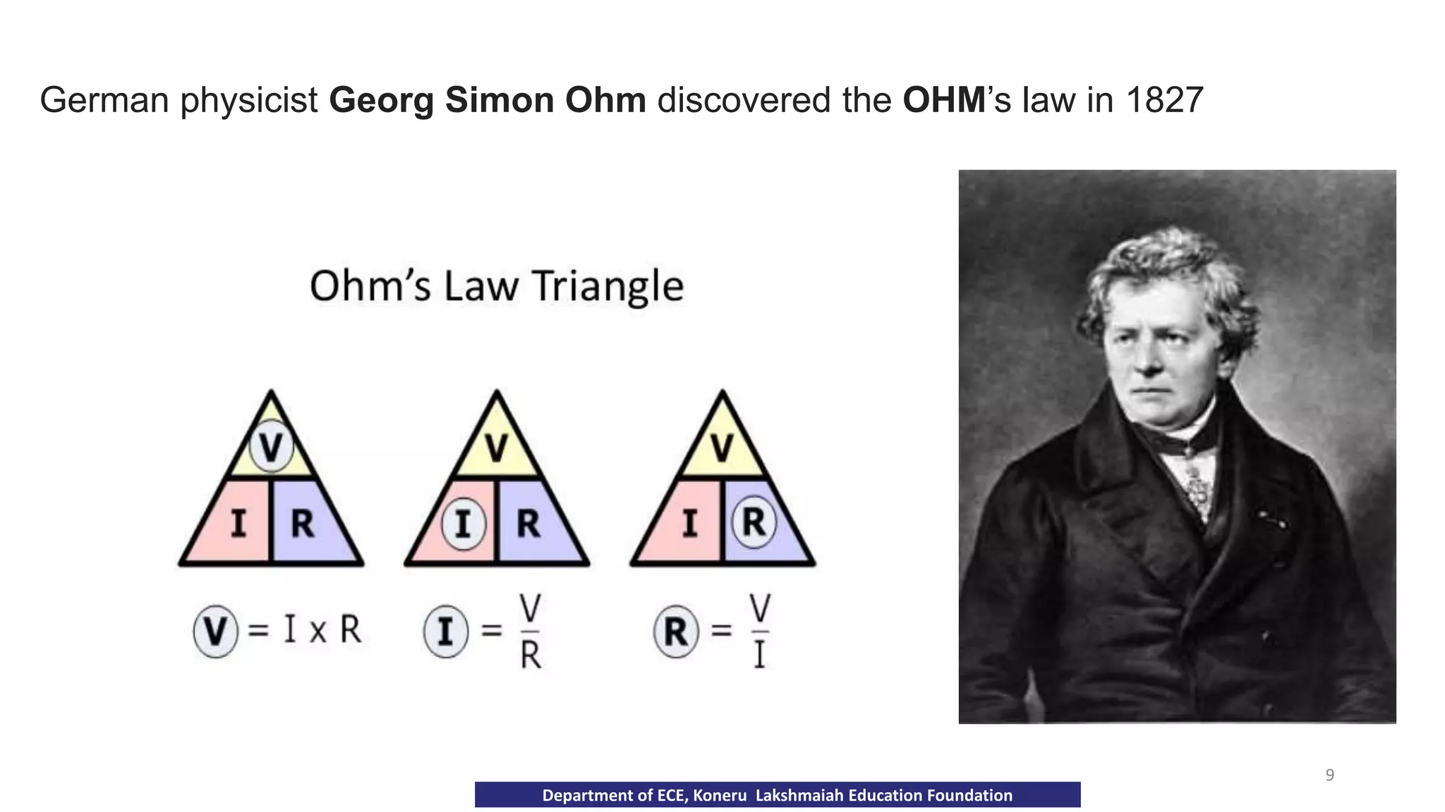
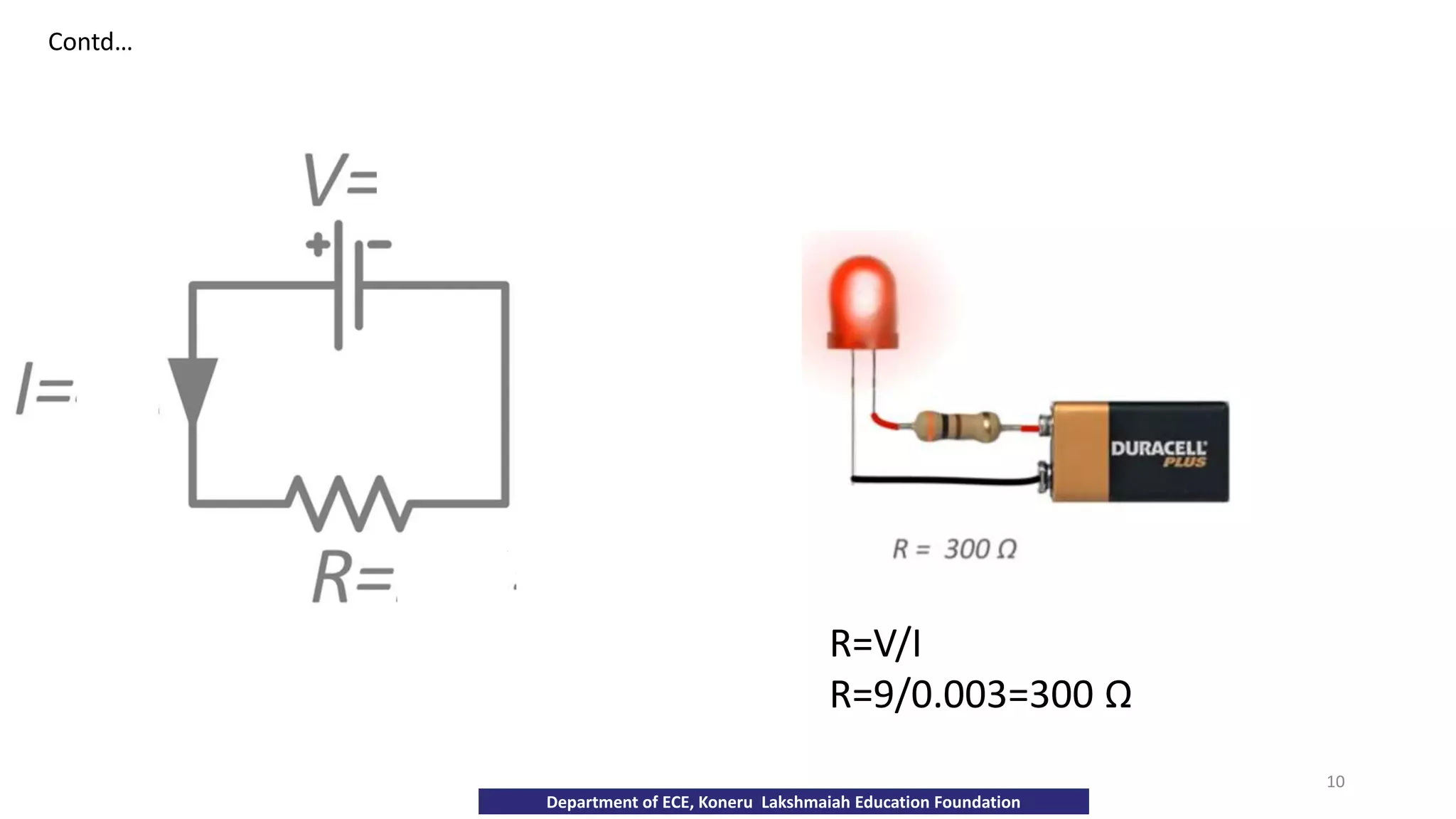
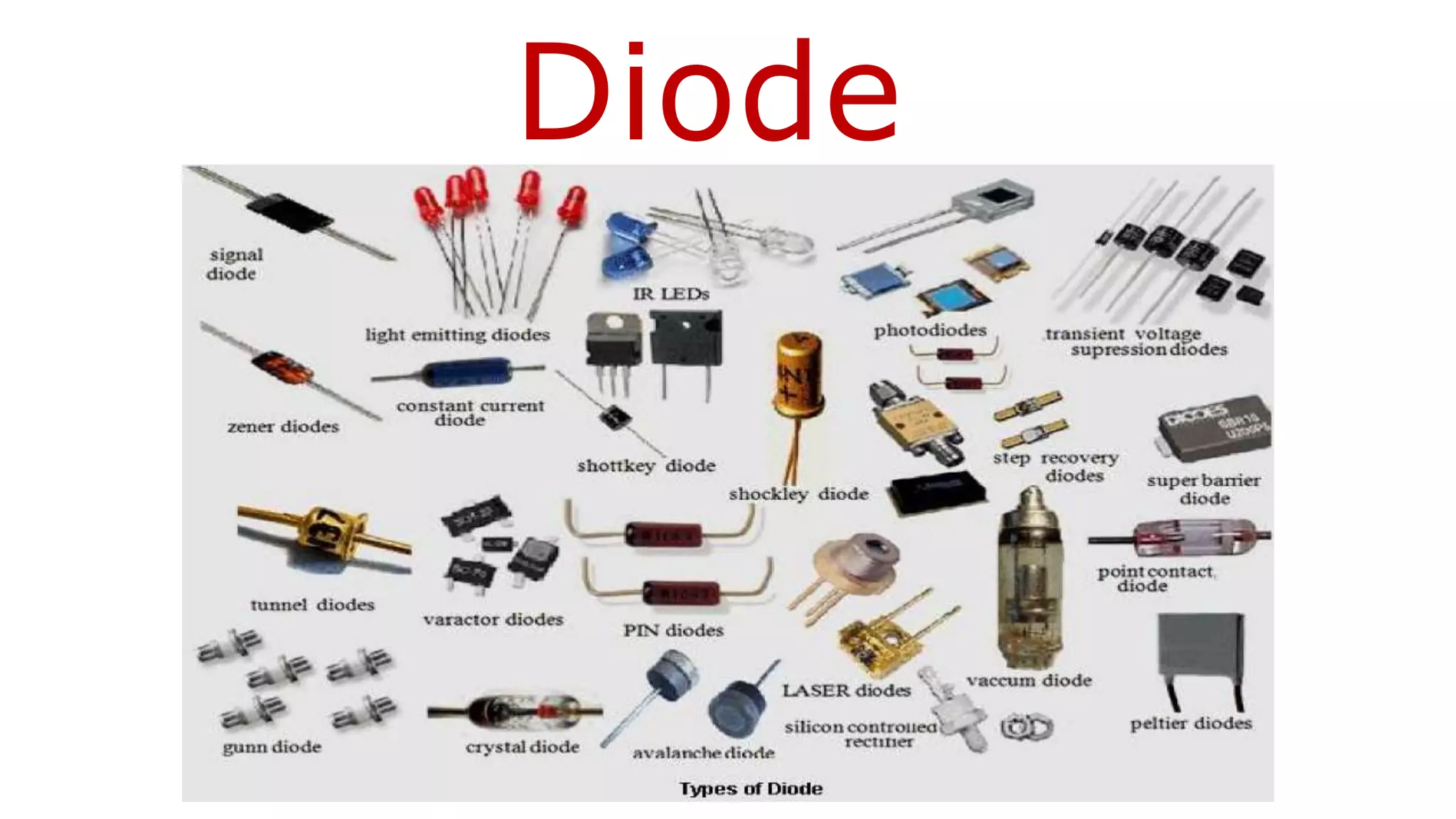
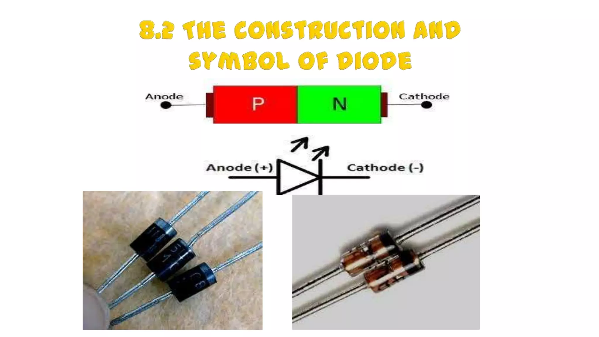
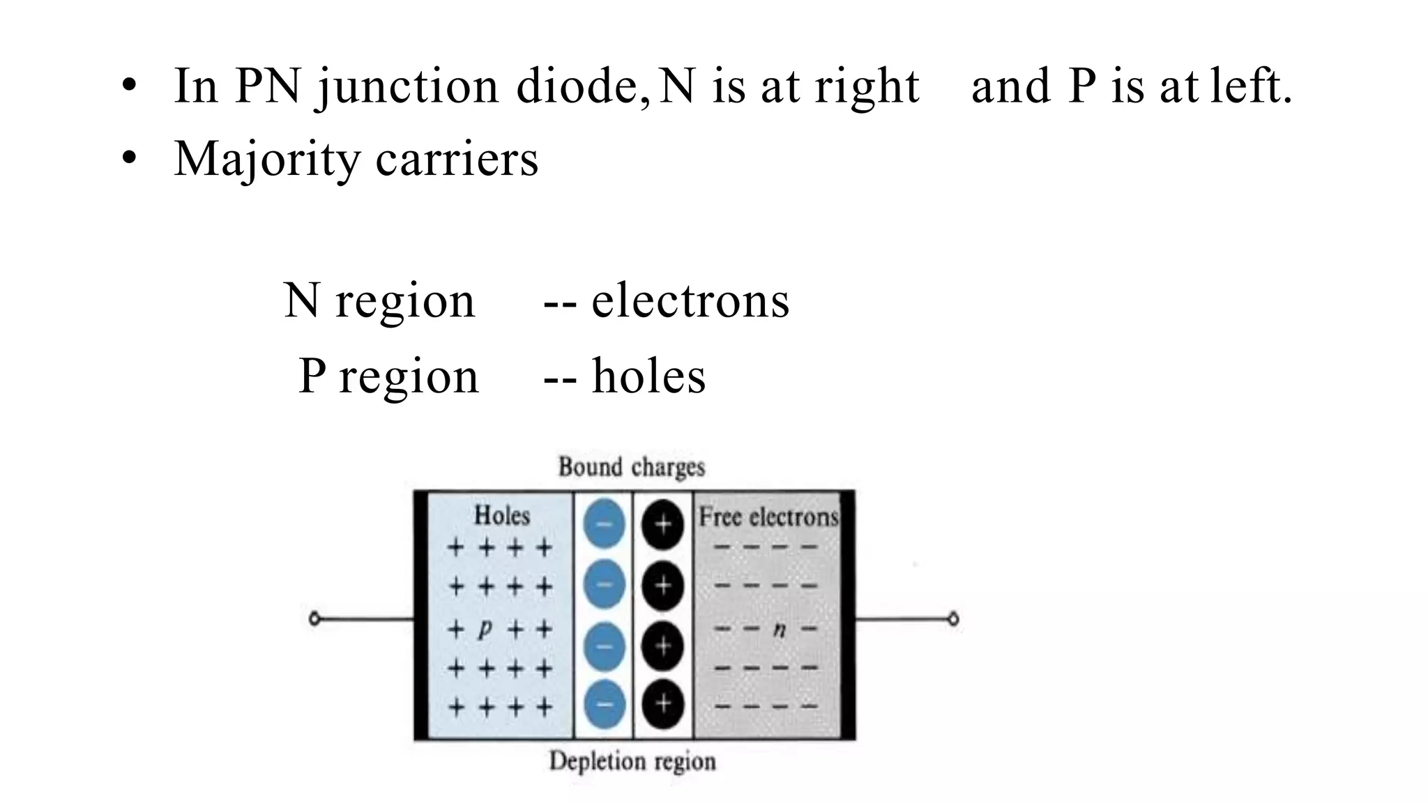


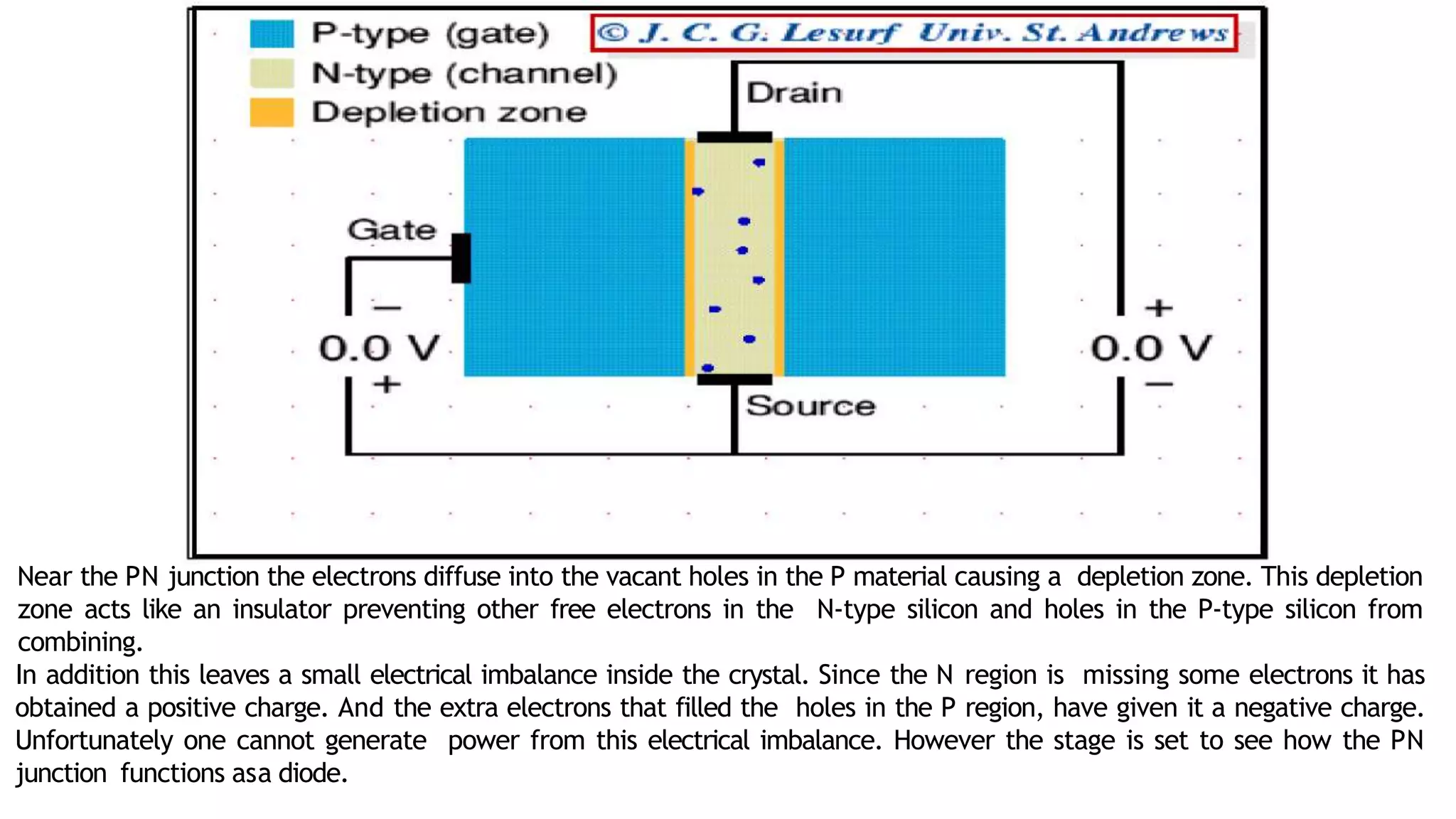

The document discusses fundamentals of electronics including passive components like resistors, capacitors, and inductors. It describes analog electronics circuits using transistors and op-amps. Digital electronics concepts like logic gates, microprocessors, RAM, and ROMs are covered. The document also provides details about diodes, their construction using P-type and N-type semiconductors to form a PN junction, and their operating characteristics in forward and reverse bias modes. Resistance and Ohm's law calculations are demonstrated.


