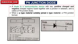
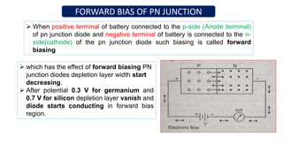
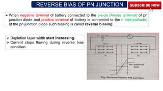
Prof.Prasant Tiwari
P-N JUNCTION DIODE
Basic Electrical & Electronics
Engineering
PN JUNCTION DIODE
 In this video, we learn about PN junction diode
characteristics in detail.
 How to bias a PN junction (Forward & Reverse bias
methods), behavior of PN junction during forward &
reverse bias.
The basic difference between a forward bias and
reverse bias is in the direction of applying external
voltage.
The direction of external voltage applied in reverse
bias is opposite to that of external voltage applied in
forward bias.
PN JUNCTION DIODE
 A diode is a semiconductor device with two, positive charged and
negative charged regions fused together with a junction in between, and is
called a P-N junction diode.
 When a p type material suitably joined n type material, a P-N junction
formed.
FORWARD BIAS OF PN JUNCTION
 When positive terminal of battery connected to the p-side (Anode terminal)
of pn junction diode and negative terminal of battery is connected to the n-
side(cathode) of the pn junction diode such biasing is called forward
biasing
 which has the effect of forward biasing PN
junction diodes depletion layer width start
decreasing.
 After potential 0.3 V for germanium and
0.7 V for silicon depletion layer vanish and
diode starts conducting in forward bias
region.
REVERSE BIAS OF PN JUNCTION
 When negative terminal of battery connected to the p-side (Anode terminal) of pn
junction diode and positive terminal of battery is connected to the n-side(cathode)
of the pn junction diode such biasing is called reverse biasing
 Depletion layer width start increasing.
 Current stops flowing during reverse bias
condition.
PLZ VISIT YPUTUBE CHANNEL FOR VIDEO
LINK IS GIVEN IN DESCRIPTION BOX

PN JUNCTION DIODE IN हिंदी|FORWARD AND REVERSE BIASED OF DIODE|BASIC ELECTRONICS|SEMICONDUCTOR DIODE

  • 1.
    Prof.Prasant Tiwari P-N JUNCTIONDIODE Basic Electrical & Electronics Engineering
  • 2.
    PN JUNCTION DIODE In this video, we learn about PN junction diode characteristics in detail.  How to bias a PN junction (Forward & Reverse bias methods), behavior of PN junction during forward & reverse bias. The basic difference between a forward bias and reverse bias is in the direction of applying external voltage. The direction of external voltage applied in reverse bias is opposite to that of external voltage applied in forward bias.
  • 3.
    PN JUNCTION DIODE A diode is a semiconductor device with two, positive charged and negative charged regions fused together with a junction in between, and is called a P-N junction diode.  When a p type material suitably joined n type material, a P-N junction formed.
  • 4.
    FORWARD BIAS OFPN JUNCTION  When positive terminal of battery connected to the p-side (Anode terminal) of pn junction diode and negative terminal of battery is connected to the n- side(cathode) of the pn junction diode such biasing is called forward biasing  which has the effect of forward biasing PN junction diodes depletion layer width start decreasing.  After potential 0.3 V for germanium and 0.7 V for silicon depletion layer vanish and diode starts conducting in forward bias region.
  • 5.
    REVERSE BIAS OFPN JUNCTION  When negative terminal of battery connected to the p-side (Anode terminal) of pn junction diode and positive terminal of battery is connected to the n-side(cathode) of the pn junction diode such biasing is called reverse biasing  Depletion layer width start increasing.  Current stops flowing during reverse bias condition.
  • 6.
    PLZ VISIT YPUTUBECHANNEL FOR VIDEO LINK IS GIVEN IN DESCRIPTION BOX