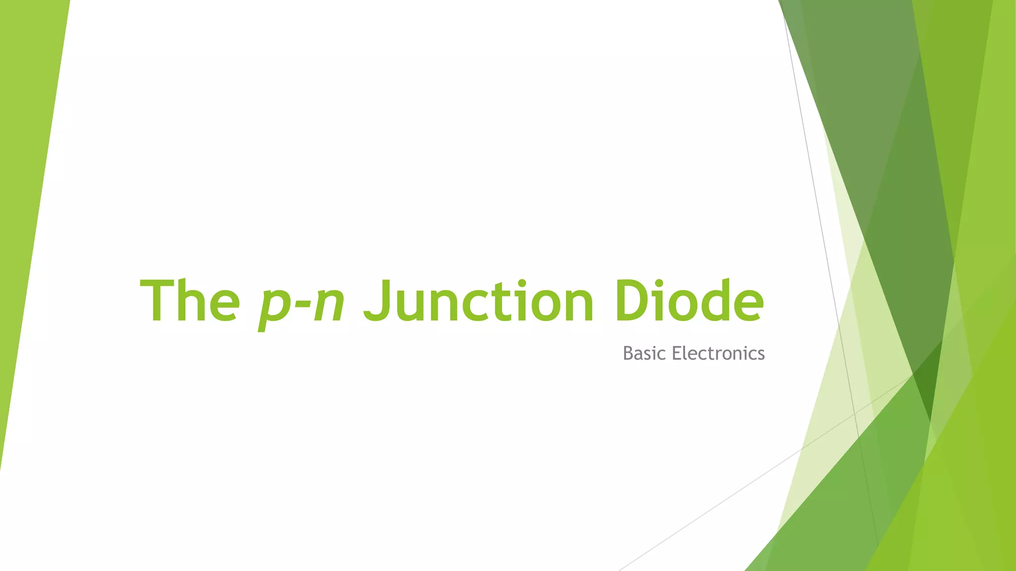
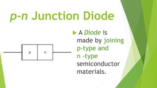
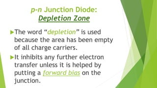
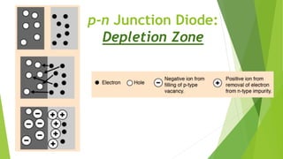
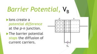
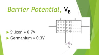
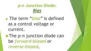
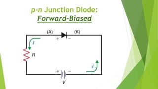
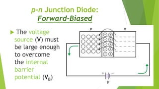
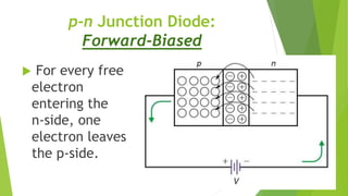
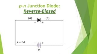
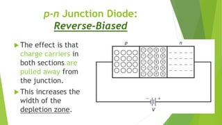
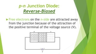
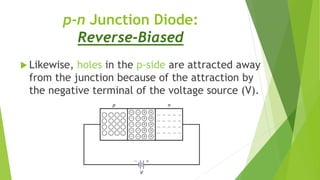
The p-n Junction Diode
Basic Electronics
p-n Junction Diode
 A Diode is
made by joining
p-type and
n -type
semiconductor
materials.
p-n Junction Diode
 Diodes are
unidirectional devices
that allow current to
flow through them in
only one direction.
 The p side of the diode
is called the anode
(A), whereas the n side
of the diode is called
the cathode (K).
p-n Junction Diode:
Depletion Zone
When a p-n junction is formed, some
of the free electrons in the n-region
diffuse across the junction and
combine with holes to form negative
ions.
In so doing they leave behind positive
ions at the donor impurity sites.
p-n Junction Diode:
Depletion Zone
The area where the positive
and negative ions are located is
called the “depletion zone”
(can also be called as depletion
layer or depletion region).
p-n Junction Diode:
Depletion Zone
The word “depletion” is used
because the area has been empty
of all charge carriers.
It inhibits any further electron
transfer unless it is helped by
putting a forward bias on the
junction.
p-n Junction Diode:
Depletion Zone
p-n Junction Diode:
Depletion Zone
Barrier Potential, VB
Ions create a
potential difference
at the p-n junction.
The barrier potential
stops the diffusion of
current carriers.
Barrier Potential, VB
 Silicon = 0.7V
 Germanium = 0.3V
p-n Junction Diode:
Bias
 The term “bias” is defined
as a control voltage or
current.
The p-n junction diode can
be forward-biased or
reverse-biased.
p-n Junction Diode:
Forward-Biased
 Forward-biasing a diode
allows current to flow
easily through the diode.
p-n Junction Diode:
Forward-Biased
p-n Junction Diode:
Forward-Biased
 The voltage
source (V) must
be large enough
to overcome
the internal
barrier
potential (VB)
p-n Junction Diode:
Forward-Biased
 For every free
electron
entering the
n-side, one
electron leaves
the p-side.
p-n Junction Diode:
Reverse-Biased
 Reverse-biasing a diode
prevents current to flow
easily through the diode.
p-n Junction Diode:
Reverse-Biased
p-n Junction Diode:
Reverse-Biased
 The effect is that
charge carriers in
both sections are
pulled away from
the junction.
 This increases the
width of the
depletion zone.
p-n Junction Diode:
Reverse-Biased
 Free electrons on the n-side are attracted away
from the junction because of the attraction of
the positive terminal of the voltage source (V).
p-n Junction Diode:
Reverse-Biased
 Likewise, holes in the p-side are attracted away
from the junction because of the attraction by
the negative terminal of the voltage source (V).
References:
 Schultz, M.E. (2011) GROB’S BASIC
ELECTRONICS (pg.828-831).1221 Avenue of
the Americas, New York, NY: The McGraw-
Hill Companies, Inc.
 Nave, R. (n.d.). P-N Junction. Retrieved
from: http://hyperphysics.phy-
astr.gsu.edu/hbase/Solids/pnjun.html#c3

Diode