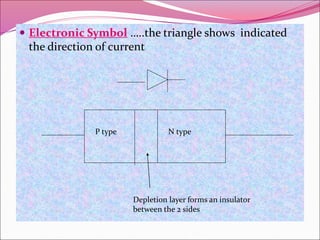
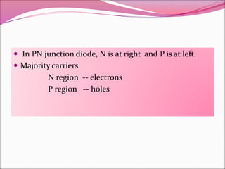
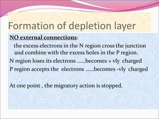
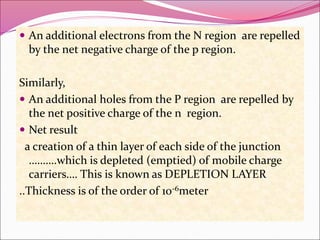
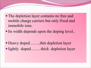
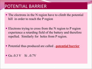
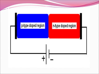
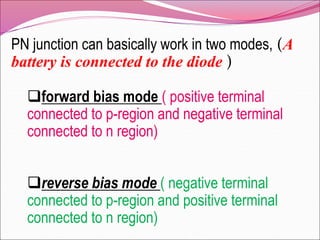
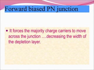
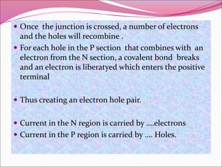
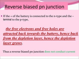
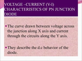
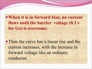
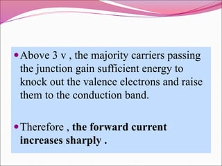
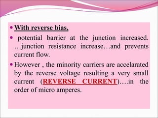
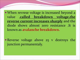
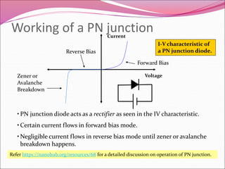
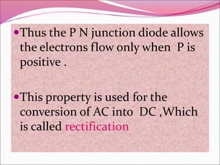
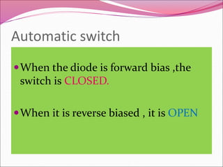
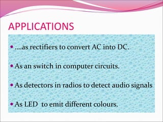
PN JUNCTION DIODE
P type and N type semiconductors, taken
separately are of very limited use.
If we join a piece of P type material to a piece
of N type material such that the crystal
structure remains continuous at the
boundary,,….. A PN JUNCTION is formed
 It can function as ….
Rectifier ,
Amplifier ,
Switching
And other operations in electronic circuits.
 A PN junction cannot be produced by simply
pushing two pieces together or by welding
etc…. Because it gives rise to discontinuities
across the crystal structure.
 Special fabrication techniques are adopted to
form a P N junction
What is a PN Junction?
A PN junction is a device
formed by joining p-type (
doped with B, Al) with n-
type (doped with P, As, Sb)
semiconductors and
separated by a thin junction
is called PN Junction diode
 Electronic Symbol …..the triangle shows indicated
the direction of current
Depletion layer forms an insulator
between the 2 sides
P type N type
 In PN junction diode, N is at right and P is at left.
 Majority carriers
N region -- electrons
P region -- holes
Formation of depletion layer
NO external connections:
the excess electrons in the N region cross the junction
and combine with the excess holes in the P region.
N region loses its electrons ……becomes + vly charged
P region accepts the electrons ……becomes -vly charged
At one point , the migratory action is stopped.
 An additional electrons from the N region are repelled
by the net negative charge of the p region.
Similarly,
 An additional holes from the P region are repelled by
the net positive charge of the n region.
 Net result
a creation of a thin layer of each side of the junction
……….which is depleted (emptied) of mobile charge
carriers…. This is known as DEPLETION LAYER
..Thickness is of the order of 10-6meter
 The depletion layer contains no free and
mobile charge carriers but only fixed and
immobile ions.
 Its width depends upon the doping level..
 Heavy doped……..thin depletion layer
 lightly doped……..thick depletion layer
POTENTIAL BARRIER
 The electrons in the N region have to climb the potential
hill in order to reach the P region
 Electrons trying to cross from the N region to P region
experience a retarding field of the battery and therefore
repelled. Similarly for holes from P region.
 Potential thus produced are called ..potential barrier
 Ge..0.3 V Si ..0.7V
PN junction can basically work in two modes, (A
battery is connected to the diode )
forward bias mode ( positive terminal
connected to p-region and negative terminal
connected to n region)
reverse bias mode ( negative terminal
connected to p-region and positive terminal
connected to n region)
Forward biased PN junction
 It forces the majority charge carriers to move
across the junction ….decreasing the width of
the depletion layer.
 Once the junction is crossed, a number of electrons
and the holes will recombine .
 For each hole in the P section that combines with an
electron from the N section, a covalent bond breaks
and an electron is liberatyed which enters the positive
terminal
 Thus creating an electron hole pair.
 Current in the N region is carried by ….electrons
 Current in the P region is carried by …. Holes.
Reverse biased pn junction
 If the + of the battery is connected to the n-type and the –
terminal to the p-type,
the free electrons and free holes are
attracted back towards the battery, hence back
from the depletion layer, hence the depletion
layer grows.
Thus a reverse biased pn junction does not conduct current
Only the minority carriers cross the
junction constituting very low
reverse saturation current.
This current is of the order of micro
ampere.
VOLTAGE –CURRENT (V-I)
CHARACTERISTICS OF PN JUNCTION
DIODE
The curve drawn between voltage across
the junction along X axis and current
through the circuits along the Y axis.
They describe the d.c behavior of the
diode.
When it is in forward bias, no current
flows until the barrier voltage (0.3 v
for Ge) is overcome.
Then the curve has a linear rise and the
current increases, with the increase in
forward voltage like an ordinary
conductor.
Above 3 v , the majority carriers passing
the junction gain sufficient energy to
knock out the valence electrons and raise
them to the conduction band.
Therefore , the forward current
increases sharply .
 With reverse bias,
 potential barrier at the junction increased.
…junction resistance increase…and prevents
current flow.
 However , the minority carriers are accelarated
by the reverse voltage resulting a very small
current (REVERSE CURRENT)….in the
order of micro amperes.
 When revrese voltage is increased beyond a
value ,called breakdown voltage,the
reverse current increases sharply and the
diode shows almost zero resistance .It is
known as avalanche breakdown.
 Reverse voltage above 25 v destroys the
junction permanentaly.
Working of a PN junction
Refer https://nanohub.org/resources/68 for a detailed discussion on operation of PN junction.
Forward Bias
Reverse Bias
Zener or
Avalanche
Breakdown
Voltage
Current
I-V characteristic of
a PN junction diode.
• PN junction diode acts as a rectifier as seen in the IV characteristic.
• Certain current flows in forward bias mode.
• Negligible current flows in reverse bias mode until zener or avalanche
breakdown happens.
Thus the P N junction diode allows
the electrons flow only when P is
positive .
This property is used for the
conversion of AC into DC ,Which
is called rectification
Automatic switch
When the diode is forward bias ,the
switch is CLOSED.
When it is reverse biased , it is OPEN
ADVANTAGES:
 No filament is necessary
 Occupies lesser space
 Long life.
APPLICATIONS
 ….as rectifiers to convert AC into DC.
 As an switch in computer circuits.
 As detectors in radios to detect audio signals
 As LED to emit different colours.

pn-junctiondiodeJJNINIIJOIOOIMOMOKMOMOIM

  • 1.
  • 2.
    P type andN type semiconductors, taken separately are of very limited use. If we join a piece of P type material to a piece of N type material such that the crystal structure remains continuous at the boundary,,….. A PN JUNCTION is formed
  • 3.
     It canfunction as …. Rectifier , Amplifier , Switching And other operations in electronic circuits.
  • 4.
     A PNjunction cannot be produced by simply pushing two pieces together or by welding etc…. Because it gives rise to discontinuities across the crystal structure.  Special fabrication techniques are adopted to form a P N junction
  • 5.
    What is aPN Junction? A PN junction is a device formed by joining p-type ( doped with B, Al) with n- type (doped with P, As, Sb) semiconductors and separated by a thin junction is called PN Junction diode
  • 6.
     Electronic Symbol…..the triangle shows indicated the direction of current Depletion layer forms an insulator between the 2 sides P type N type
  • 7.
     In PNjunction diode, N is at right and P is at left.  Majority carriers N region -- electrons P region -- holes
  • 8.
    Formation of depletionlayer NO external connections: the excess electrons in the N region cross the junction and combine with the excess holes in the P region. N region loses its electrons ……becomes + vly charged P region accepts the electrons ……becomes -vly charged At one point , the migratory action is stopped.
  • 9.
     An additionalelectrons from the N region are repelled by the net negative charge of the p region. Similarly,  An additional holes from the P region are repelled by the net positive charge of the n region.  Net result a creation of a thin layer of each side of the junction ……….which is depleted (emptied) of mobile charge carriers…. This is known as DEPLETION LAYER ..Thickness is of the order of 10-6meter
  • 10.
     The depletionlayer contains no free and mobile charge carriers but only fixed and immobile ions.  Its width depends upon the doping level..  Heavy doped……..thin depletion layer  lightly doped……..thick depletion layer
  • 11.
    POTENTIAL BARRIER  Theelectrons in the N region have to climb the potential hill in order to reach the P region  Electrons trying to cross from the N region to P region experience a retarding field of the battery and therefore repelled. Similarly for holes from P region.  Potential thus produced are called ..potential barrier  Ge..0.3 V Si ..0.7V
  • 13.
    PN junction canbasically work in two modes, (A battery is connected to the diode ) forward bias mode ( positive terminal connected to p-region and negative terminal connected to n region) reverse bias mode ( negative terminal connected to p-region and positive terminal connected to n region)
  • 14.
    Forward biased PNjunction  It forces the majority charge carriers to move across the junction ….decreasing the width of the depletion layer.
  • 15.
     Once thejunction is crossed, a number of electrons and the holes will recombine .  For each hole in the P section that combines with an electron from the N section, a covalent bond breaks and an electron is liberatyed which enters the positive terminal  Thus creating an electron hole pair.  Current in the N region is carried by ….electrons  Current in the P region is carried by …. Holes.
  • 16.
    Reverse biased pnjunction  If the + of the battery is connected to the n-type and the – terminal to the p-type, the free electrons and free holes are attracted back towards the battery, hence back from the depletion layer, hence the depletion layer grows. Thus a reverse biased pn junction does not conduct current
  • 17.
    Only the minoritycarriers cross the junction constituting very low reverse saturation current. This current is of the order of micro ampere.
  • 18.
    VOLTAGE –CURRENT (V-I) CHARACTERISTICSOF PN JUNCTION DIODE The curve drawn between voltage across the junction along X axis and current through the circuits along the Y axis. They describe the d.c behavior of the diode.
  • 19.
    When it isin forward bias, no current flows until the barrier voltage (0.3 v for Ge) is overcome. Then the curve has a linear rise and the current increases, with the increase in forward voltage like an ordinary conductor.
  • 20.
    Above 3 v, the majority carriers passing the junction gain sufficient energy to knock out the valence electrons and raise them to the conduction band. Therefore , the forward current increases sharply .
  • 21.
     With reversebias,  potential barrier at the junction increased. …junction resistance increase…and prevents current flow.  However , the minority carriers are accelarated by the reverse voltage resulting a very small current (REVERSE CURRENT)….in the order of micro amperes.
  • 22.
     When revresevoltage is increased beyond a value ,called breakdown voltage,the reverse current increases sharply and the diode shows almost zero resistance .It is known as avalanche breakdown.  Reverse voltage above 25 v destroys the junction permanentaly.
  • 23.
    Working of aPN junction Refer https://nanohub.org/resources/68 for a detailed discussion on operation of PN junction. Forward Bias Reverse Bias Zener or Avalanche Breakdown Voltage Current I-V characteristic of a PN junction diode. • PN junction diode acts as a rectifier as seen in the IV characteristic. • Certain current flows in forward bias mode. • Negligible current flows in reverse bias mode until zener or avalanche breakdown happens.
  • 24.
    Thus the PN junction diode allows the electrons flow only when P is positive . This property is used for the conversion of AC into DC ,Which is called rectification
  • 25.
    Automatic switch When thediode is forward bias ,the switch is CLOSED. When it is reverse biased , it is OPEN
  • 26.
    ADVANTAGES:  No filamentis necessary  Occupies lesser space  Long life.
  • 27.
    APPLICATIONS  ….as rectifiersto convert AC into DC.  As an switch in computer circuits.  As detectors in radios to detect audio signals  As LED to emit different colours.