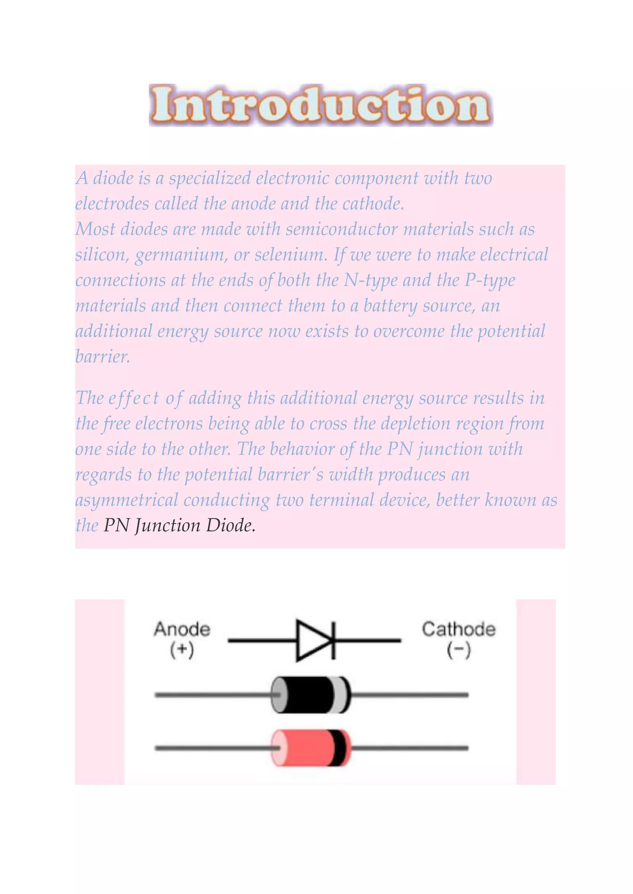
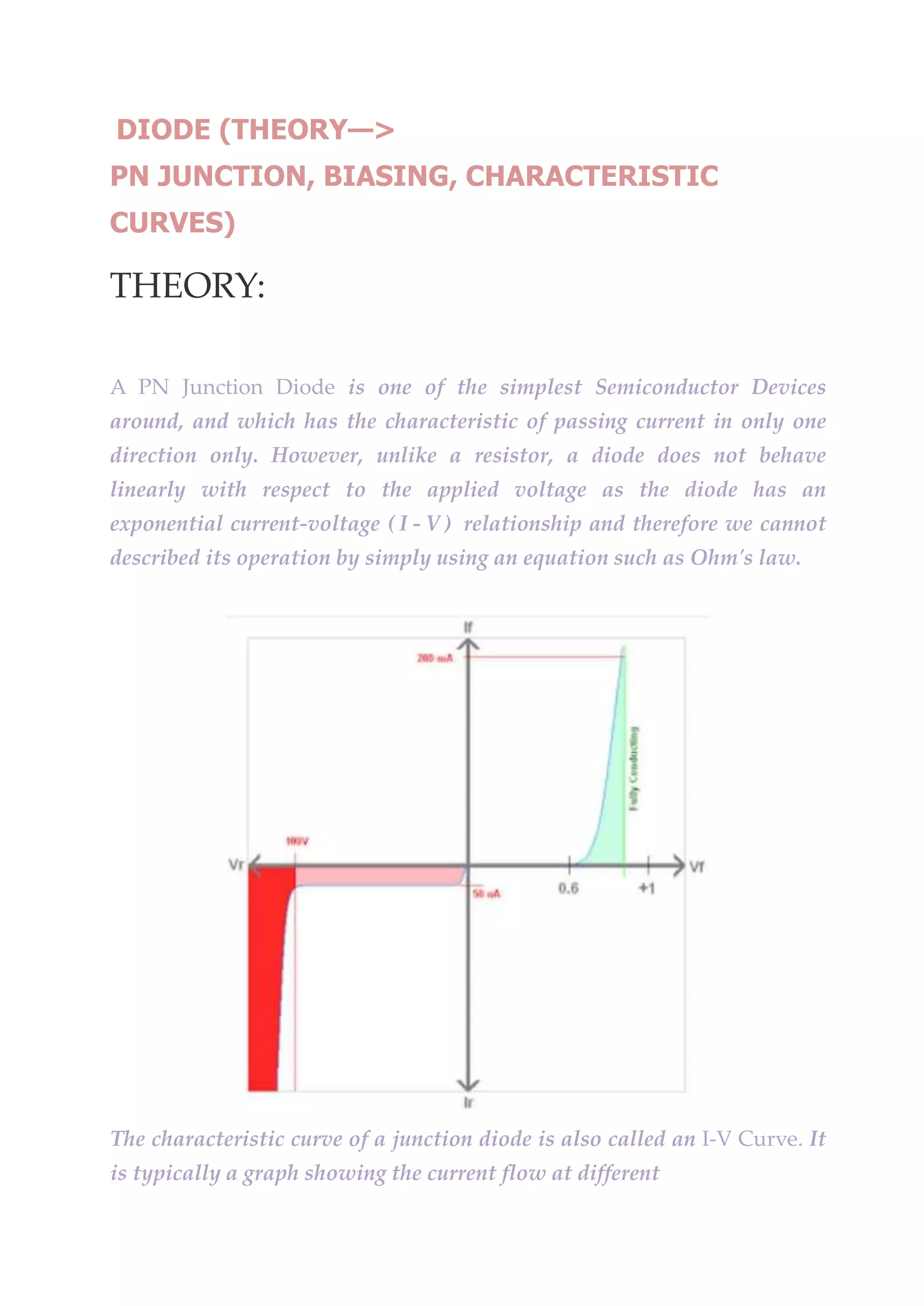
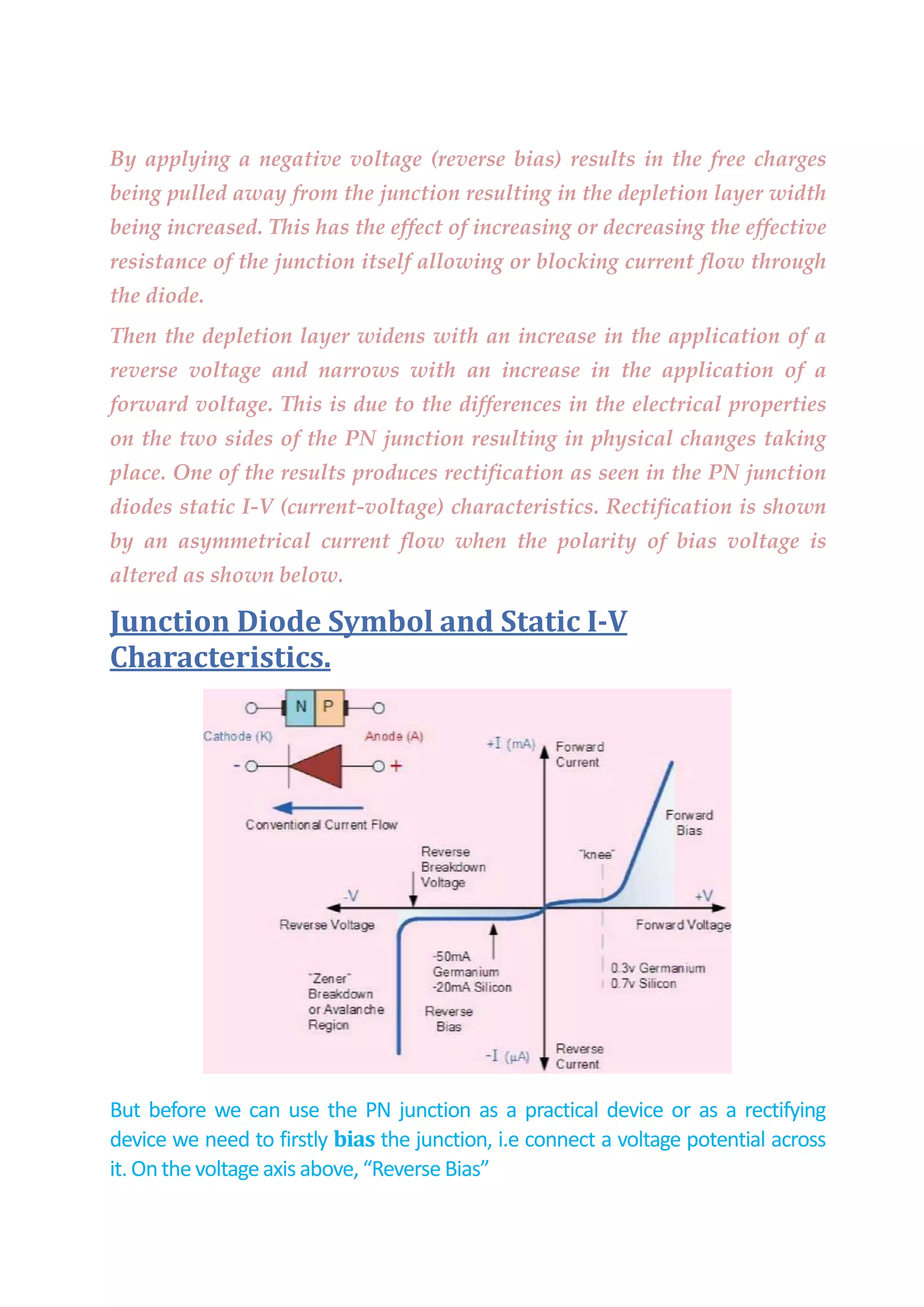
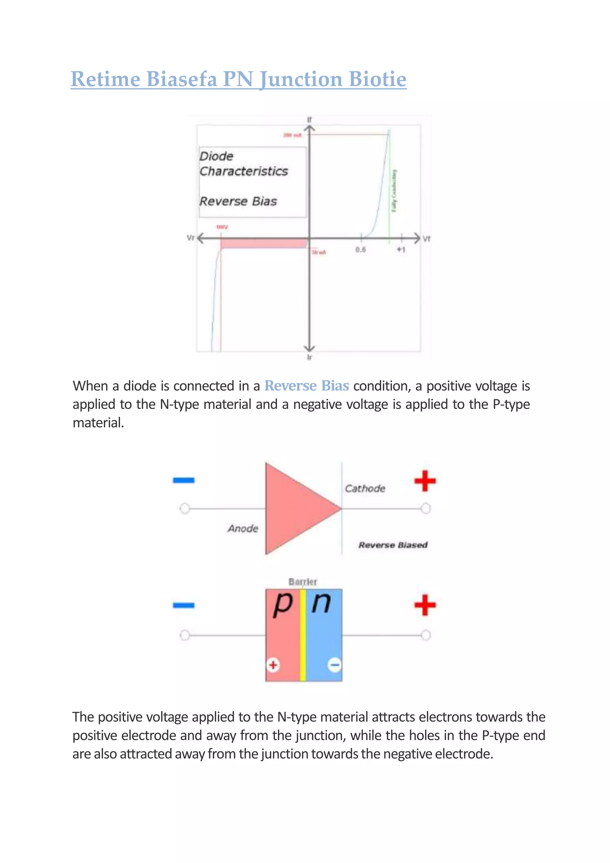
Physics Investigatory Project
Report
P-N JUNCTION DIODE
(SESSION 2019-2020)
PROJECT BY :-
ABHIJEET KUMAR SINGH
XII- ‘A’
MR.N.K.Pandey PGT (PHYSICS)
KENDRIYA VIDYALAYA NO.1 KANAKARBAGH
As usual a (large number of people deserve my thanks for
the help they provided me for the preparation of this
project.
first of all I would
like to thank my teacher MR. N.K.Pandey Sir for his
support during the preparation of this project. I am very
thankful for his guidance.
I would also like to thank my friends for the
encouragement and information about the topic they
provided to me during my efforts to prepare this topic.
At last but not the least I would like to thank seniors for
providing me their experience and being with me during
my work.
This is to certify that Abhijeet Kumar Singh,
Class:- XII ‘A’ of Kendriya Vidyalaya No. -1 Kankarbagh
Patna-20 successfully completed his project in physics
subject as prescribed by CBSE in year 2019-20.
This project is absolutely genuine and does not indulge in
plagiarism of any kind. The references taken in making this
project have been declared at the end of this project.
Date:
Registration No.:
Signature Signature
(Subject Teacher) (Examiner)
CONTENTS
1. Certificate
2. Acknowledgement
3. Introduction
4. Diode Theory
5. Zero Biased Junction Diode
6. Reverse Biased PN Junction Diode
7. Forward Biased PN Junction Diode
8. Breakdown Region
9. Useful Diode Parameters
10. Junction Diode Ideal and Real Characteristics
11. Bibliography
12. Websites
A diode is a specialized electronic component with two
electrodes called the anode and the cathode.
Most diodes are made with semiconductor materials such as
silicon, germanium, or selenium. If we were to make electrical
connections at the ends of both the N-type and the P-type
materials and then connect them to a battery source, an
additional energy source now exists to overcome the potential
barrier.
The effect of adding this additional energy source results in
the free electrons being able to cross the depletion region from
one side to the other. The behavior of the PN junction with
regards to the potential barrier's width produces an
asymmetrical conducting two terminal device, better known as
the PN Junction Diode.
DIODE (THEORY—>
PN JUNCTION, BIASING, CHARACTERISTIC
CURVES)
THEORY:
A PN Junction Diode is one of the simplest Semiconductor Devices
around, and which has the characteristic of passing current in only one
direction only. However, unlike a resistor, a diode does not behave
linearly with respect to the applied voltage as the diode has an
exponential current-voltage ( I - V ) relationship and therefore we cannot
described its operation by simply using an equation such as Ohm's law.
The characteristic curve of a junction diode is also called an I-V Curve. It
is typically a graph showing the current flow at different
voltages. The current is typically on the y-axis, and the voltage on the x-
axis. This type of graph provides engineers with a visual record of the
operating characteristics of the component. This information enables
them to use the component more appropriately within a circuit. There are
many different types of diodes, and they all have different characteristics
curves and applications. Here are some diodes you might come across:
Zener, Germanium, Gunn, Tunnel, and Schottky. The current that flows
through it is not proportional to the applied voltage.
IT
J
Compmat-H Stale
y / /
Forward
Current
Forward
Voltage
1 L V
^ /V" 1 1 >
Reverse
0,& +1
Voltage
Reverse
Current yftr
If a suitable positive voltage (forward bias) is applied between the two
ends of the PN junction, it can supply free electrons and holes with the
extra energy they require to cross the junction as the width of the
depletion layer around the PN junction is decreased.
By applying a negative voltage (reverse bias) results in the free charges
being pulled away from the junction resulting in the depletion layer width
being increased. This has the effect of increasing or decreasing the effective
resistance of the junction itself allowing or blocking current flow through
the diode.
Then the depletion layer widens with an increase in the application of a
reverse voltage and narrows with an increase in the application of a
forward voltage. This is due to the differences in the electrical properties
on the two sides of the PN junction resulting in physical changes taking
place. One of the results produces rectification as seen in the PN junction
diodes static I-V (current-voltage) characteristics. Rectification is shown
by an asymmetrical current flow when the polarity of bias voltage is
altered as shown below.
Junction Diode Symbol and Static I-V
Characteristics.
But before we can use the PN junction as a practical device or as a rectifying
device we need to firstly bias the junction, i.e connect a voltage potential across
it. Onthe voltageaxis above, “Reverse Bias”
refers to an external voltage potential which increases the potential barrier. An
external voltage which decreases the potential barrier is said to act in the
“ForwardBias”direction.
There are two operating regions and three possible “biasing” conditions for
the standard Junction Diode and these are:
• l.Zero Bias - No external voltage potential is applied to the PN
junction diode.
• 2.Reverse Bias - The voltage potential is connected negative, (-ve) to
the P-type material and positive, (+ve) to the N-type material across the
diode which has the effect of Increasing the PN junction diode's width.
• 3.Forward Bias - The voltage potential is connected positive, (+ve) to
the P-type material and negative, (-ve) to the N-type material across the
diode which has the effect of Decreasing the PN junction diodes width.
Zero Biased Junction Diode
When a diode is connected in a Zero Bias condition, no external potential
energy is applied to the PN junction. However if the diodes terminals are
shorted together, a few holes (majority carriers) in the P-type material
with enough energy to overcome the potential barrier will move across
the junction against this barrier potential. This is known as the “Forward
Current” and is referenced as IF
Likewise, holes generated in the N-type material (minority carriers), find
this situation favorable and move across the junction in the opposite
direction. This is known as the “Reverse Current” and is referenced as
IR. This transfer of electrons and holes back and forth across the PN
junction is known as diffusion, as shown below.
ZeroBiasedPN JunctionDtobe
The potential barrier that now exists discourages the diffusion of any more
majority carriers across the junction. However, the potential barrier helps minority
carriers (few free electrons in the P-region and few holes in the N-region) to drift
acrossthe junction.
Then an “Equilibrium” or balance will be established when the majority carriers
are equal and both moving in opposite directions, so that the net result is zero
current flowing in the circuit. When this occurs the junction is said to be in a state
of “Dynamic Equilibrium*.
The minority carriers are constantly generated due to thermal energy so this state
of equilibrium can be broken by raising the temperature of the PN junction
causing an increase in the generation of minority carriers, thereby resulting in an
increase in leakage current but an electric current cannot flow since no circuit has
been connectedto the PNjunction.
Retime Biasefa PN Junction Biotie
When a diode is connected in a Reverse Bias condition, a positive voltage is
applied to the N-type material and a negative voltage is applied to the P-type
material.
The positive voltage applied to the N-type material attracts electrons towards the
positive electrode and away from the junction, while the holes in the P-type end
arealso attractedawayfrom the junctiontowardsthenegativeelectrode.
The net result is that the depletion layer grows wider due to a lack of electrons
and holes and presents a high impedance path, almost an insulator. The result is
that a high potential barrier is created thus preventing current from flowing
throughthe semiconductormaterial.
Increase in the Depletion Layer due to Reverse Bias
PN-junction
rl
N-region I
D-region
- -
+ +
1
+
+ +
1
+ t +
1
1
+ + +
+ +
wider depletion
layer ' #-
4Jl- - ll '
h
AA/V I = 0
Reverse Biasing Voltage
This condition represents a high resistance value to the PN junction and practically zero
current flows through the junction diode with an increase in bias voltage. However, a very
small leakage current does flow through the junction which can be measured in micro-
amperes, ( |JA ).
One final point, if the reverse bias voltage Vr applied to the diode is increased to a sufficiently
high enough value, it will cause the diode’s PN junction to overheat and fail due to the
avalanche effect around the junction. This may cause the diode to become shorted and will
resultin the flow of maximum circuit current, and this shown as a step downward slope in the
reverse static characteristics curve below.
Reverse Characteristics Curve for a Junction
Diode
Sometimes this avalanche effect has practical applications in voltage
stabilizing circuits where a series limiting resistor is used with the diode to
limit this reverse breakdown current to a preset maximum value thereby
producing a fixed voltage output across the diode. These types of diodes
are commonly known as Zener Diodes and are discussed in a later tutorial.
Forward Biased PN Junction Diode
When a diode isconnected ina Forward Bias condition, a negative voltage isapplied to the
N-type material and apositive voltage isapplied to the P-type material. If this external
voltage becomes greater than the value of the potential barrier, approx. 0.7 volts for silicon
and 0.3 volts for germanium, the potential barriers opposition will be overcome and current
will start to flow.
This is because the negative voltage pushes or repels electrons towards the junction
giving them the energy to cross over and combine with the holes being pushed in the
opposite direction towards the junction by the positive voltage. This results in a
characteristics curve of zero current flowing up to this voltage point, called the
“knee” on the static curves and then a high current flow through the diode with little
increase in the external voltage as shown below.
Forward Characteristics Curde for a Junction
Diode
The application of a forward biasing voltage on the junction diode results in the
depletion layer becoming very thin and narrow which represents a low impedance
path through the junction thereby allowing high currents to flow. The point at which
this sudden increase in current takes place is represented on
Forward Current
IFHIA
knee
Silicon
Diode
Forward
Bias
Region
Forward Voltage, i Vp volts I
the static I-V characteristics curve above as the “knee” point.
Reduction in the Depletion Layer tone to
Fortoard Bias
This condition represents the low resistance path through the PN junction
allowing very large currents to flow through the diode with only a small increase in
bias voltage. The actual potential difference across the junction or diode is kept
constant by the action of the depletion layer at approximately 0.3v for germanium
andapproximately0.7v for siliconjunctiondiodes.
Since the diode can conduct “infinite” current above this knee point as it
effectively becomes a short circuit, therefore resistors are used in series with the
diode to limit its current flow. Exceeding its maximum forward current
specification causes the device to dissipate more power in the form of heat than it
was designedfor resultingin a veryquick failureof thedevice.
We have also seen above that the diode is two terminal non-linear device whose I-
V characteristic are polarity dependent as depending upon the polarity of the
applied voltage, VD the diode is either ForwardBiased, VD > 0 or ReverseBiased,
VD < 0. Either way we can model these current-voltage characteristics for both an
ideal diodeandfor a real diode.
Breakboton Region
Then something interesting happens at the knee part of the
curve. This point is called the breakdown voltage. Suddenly there
is an increased flow in reverse current. No matter how much
reverse voltage is applied, the voltage across the diode does not
change.
In specification sheets some manufacturers refer to the reverse
current, or leakage current, as the point near the knee, just
before breakdown occurs.
Useful Diode Parameters
The maximum forward bias current (If) of a diode is a very
useful parameter. Different diodes are capable of carrying
different amount of current. If you are placing a protection diode
into a circuit, you will need to know how much current your
circuit will draw, and whether the diode is up to the job of
carrying it.
The forward voltage drop (Vf), also known as the cut-off voltage,
is a very useful parameter worth knowing. This parameter is
defined at a specified current and temperature in datasheets.
This value tells you that the diode will continue conducting even
when the voltage falls as low as that figure.
What most people do not realize is that the forward voltage drop
is ideally specified when the forward current is zero. This is when
the curve cuts the x-axis and the current is zero.
If you were a crystal radio enthusiast, you would be interested in
this parameter because it determines how sensitive your crystal
radio diode is.
Diodes are Very sensitive to heat and their resistance can change
creating a drift. This is Why datasheets always mention the parameters
taken at a specific temperature. Typically it is at 25 °C.
JunctionDiode IdealandRealCharacteristics
1. Physics NCERT Textbook
2. Fundamental Physics - Pradeep Kshetrapal
3. Concept of Physics - H.C. Verma
4. Principles of Physics - V.K. Mehta
Websites:
1. www.google.co.in
2. www.slideshare.net
3. www.scribd.com
4. www.seminars.net

Pn junction diode class 12 investegatory project

  • 1.
    Physics Investigatory Project Report P-NJUNCTION DIODE (SESSION 2019-2020) PROJECT BY :- ABHIJEET KUMAR SINGH XII- ‘A’ MR.N.K.Pandey PGT (PHYSICS) KENDRIYA VIDYALAYA NO.1 KANAKARBAGH
  • 2.
    As usual a(large number of people deserve my thanks for the help they provided me for the preparation of this project. first of all I would like to thank my teacher MR. N.K.Pandey Sir for his support during the preparation of this project. I am very thankful for his guidance. I would also like to thank my friends for the encouragement and information about the topic they provided to me during my efforts to prepare this topic. At last but not the least I would like to thank seniors for providing me their experience and being with me during my work.
  • 3.
    This is tocertify that Abhijeet Kumar Singh, Class:- XII ‘A’ of Kendriya Vidyalaya No. -1 Kankarbagh Patna-20 successfully completed his project in physics subject as prescribed by CBSE in year 2019-20. This project is absolutely genuine and does not indulge in plagiarism of any kind. The references taken in making this project have been declared at the end of this project. Date: Registration No.: Signature Signature (Subject Teacher) (Examiner)
  • 4.
    CONTENTS 1. Certificate 2. Acknowledgement 3.Introduction 4. Diode Theory 5. Zero Biased Junction Diode 6. Reverse Biased PN Junction Diode 7. Forward Biased PN Junction Diode 8. Breakdown Region 9. Useful Diode Parameters 10. Junction Diode Ideal and Real Characteristics 11. Bibliography 12. Websites
  • 5.
    A diode isa specialized electronic component with two electrodes called the anode and the cathode. Most diodes are made with semiconductor materials such as silicon, germanium, or selenium. If we were to make electrical connections at the ends of both the N-type and the P-type materials and then connect them to a battery source, an additional energy source now exists to overcome the potential barrier. The effect of adding this additional energy source results in the free electrons being able to cross the depletion region from one side to the other. The behavior of the PN junction with regards to the potential barrier's width produces an asymmetrical conducting two terminal device, better known as the PN Junction Diode.
  • 6.
    DIODE (THEORY—> PN JUNCTION,BIASING, CHARACTERISTIC CURVES) THEORY: A PN Junction Diode is one of the simplest Semiconductor Devices around, and which has the characteristic of passing current in only one direction only. However, unlike a resistor, a diode does not behave linearly with respect to the applied voltage as the diode has an exponential current-voltage ( I - V ) relationship and therefore we cannot described its operation by simply using an equation such as Ohm's law. The characteristic curve of a junction diode is also called an I-V Curve. It is typically a graph showing the current flow at different
  • 7.
    voltages. The currentis typically on the y-axis, and the voltage on the x- axis. This type of graph provides engineers with a visual record of the operating characteristics of the component. This information enables them to use the component more appropriately within a circuit. There are many different types of diodes, and they all have different characteristics curves and applications. Here are some diodes you might come across: Zener, Germanium, Gunn, Tunnel, and Schottky. The current that flows through it is not proportional to the applied voltage. IT J Compmat-H Stale y / / Forward Current Forward Voltage 1 L V ^ /V" 1 1 > Reverse 0,& +1 Voltage Reverse Current yftr If a suitable positive voltage (forward bias) is applied between the two ends of the PN junction, it can supply free electrons and holes with the extra energy they require to cross the junction as the width of the depletion layer around the PN junction is decreased.
  • 8.
    By applying anegative voltage (reverse bias) results in the free charges being pulled away from the junction resulting in the depletion layer width being increased. This has the effect of increasing or decreasing the effective resistance of the junction itself allowing or blocking current flow through the diode. Then the depletion layer widens with an increase in the application of a reverse voltage and narrows with an increase in the application of a forward voltage. This is due to the differences in the electrical properties on the two sides of the PN junction resulting in physical changes taking place. One of the results produces rectification as seen in the PN junction diodes static I-V (current-voltage) characteristics. Rectification is shown by an asymmetrical current flow when the polarity of bias voltage is altered as shown below. Junction Diode Symbol and Static I-V Characteristics. But before we can use the PN junction as a practical device or as a rectifying device we need to firstly bias the junction, i.e connect a voltage potential across it. Onthe voltageaxis above, “Reverse Bias”
  • 9.
    refers to anexternal voltage potential which increases the potential barrier. An external voltage which decreases the potential barrier is said to act in the “ForwardBias”direction. There are two operating regions and three possible “biasing” conditions for the standard Junction Diode and these are: • l.Zero Bias - No external voltage potential is applied to the PN junction diode. • 2.Reverse Bias - The voltage potential is connected negative, (-ve) to the P-type material and positive, (+ve) to the N-type material across the diode which has the effect of Increasing the PN junction diode's width. • 3.Forward Bias - The voltage potential is connected positive, (+ve) to the P-type material and negative, (-ve) to the N-type material across the diode which has the effect of Decreasing the PN junction diodes width. Zero Biased Junction Diode When a diode is connected in a Zero Bias condition, no external potential energy is applied to the PN junction. However if the diodes terminals are shorted together, a few holes (majority carriers) in the P-type material with enough energy to overcome the potential barrier will move across the junction against this barrier potential. This is known as the “Forward Current” and is referenced as IF Likewise, holes generated in the N-type material (minority carriers), find this situation favorable and move across the junction in the opposite direction. This is known as the “Reverse Current” and is referenced as IR. This transfer of electrons and holes back and forth across the PN junction is known as diffusion, as shown below.
  • 10.
    ZeroBiasedPN JunctionDtobe The potentialbarrier that now exists discourages the diffusion of any more majority carriers across the junction. However, the potential barrier helps minority carriers (few free electrons in the P-region and few holes in the N-region) to drift acrossthe junction. Then an “Equilibrium” or balance will be established when the majority carriers are equal and both moving in opposite directions, so that the net result is zero current flowing in the circuit. When this occurs the junction is said to be in a state of “Dynamic Equilibrium*. The minority carriers are constantly generated due to thermal energy so this state of equilibrium can be broken by raising the temperature of the PN junction causing an increase in the generation of minority carriers, thereby resulting in an increase in leakage current but an electric current cannot flow since no circuit has been connectedto the PNjunction.
  • 11.
    Retime Biasefa PNJunction Biotie When a diode is connected in a Reverse Bias condition, a positive voltage is applied to the N-type material and a negative voltage is applied to the P-type material. The positive voltage applied to the N-type material attracts electrons towards the positive electrode and away from the junction, while the holes in the P-type end arealso attractedawayfrom the junctiontowardsthenegativeelectrode.
  • 12.
    The net resultis that the depletion layer grows wider due to a lack of electrons and holes and presents a high impedance path, almost an insulator. The result is that a high potential barrier is created thus preventing current from flowing throughthe semiconductormaterial. Increase in the Depletion Layer due to Reverse Bias PN-junction rl N-region I D-region - - + + 1 + + + 1 + t + 1 1 + + + + + wider depletion layer ' #- 4Jl- - ll ' h AA/V I = 0 Reverse Biasing Voltage This condition represents a high resistance value to the PN junction and practically zero current flows through the junction diode with an increase in bias voltage. However, a very small leakage current does flow through the junction which can be measured in micro- amperes, ( |JA ). One final point, if the reverse bias voltage Vr applied to the diode is increased to a sufficiently high enough value, it will cause the diode’s PN junction to overheat and fail due to the avalanche effect around the junction. This may cause the diode to become shorted and will resultin the flow of maximum circuit current, and this shown as a step downward slope in the reverse static characteristics curve below.
  • 13.
    Reverse Characteristics Curvefor a Junction Diode Sometimes this avalanche effect has practical applications in voltage stabilizing circuits where a series limiting resistor is used with the diode to limit this reverse breakdown current to a preset maximum value thereby producing a fixed voltage output across the diode. These types of diodes are commonly known as Zener Diodes and are discussed in a later tutorial. Forward Biased PN Junction Diode
  • 14.
    When a diodeisconnected ina Forward Bias condition, a negative voltage isapplied to the N-type material and apositive voltage isapplied to the P-type material. If this external voltage becomes greater than the value of the potential barrier, approx. 0.7 volts for silicon and 0.3 volts for germanium, the potential barriers opposition will be overcome and current will start to flow. This is because the negative voltage pushes or repels electrons towards the junction giving them the energy to cross over and combine with the holes being pushed in the opposite direction towards the junction by the positive voltage. This results in a characteristics curve of zero current flowing up to this voltage point, called the “knee” on the static curves and then a high current flow through the diode with little increase in the external voltage as shown below. Forward Characteristics Curde for a Junction Diode The application of a forward biasing voltage on the junction diode results in the depletion layer becoming very thin and narrow which represents a low impedance path through the junction thereby allowing high currents to flow. The point at which this sudden increase in current takes place is represented on Forward Current IFHIA knee Silicon Diode Forward Bias Region Forward Voltage, i Vp volts I
  • 15.
    the static I-Vcharacteristics curve above as the “knee” point. Reduction in the Depletion Layer tone to Fortoard Bias This condition represents the low resistance path through the PN junction allowing very large currents to flow through the diode with only a small increase in bias voltage. The actual potential difference across the junction or diode is kept constant by the action of the depletion layer at approximately 0.3v for germanium andapproximately0.7v for siliconjunctiondiodes. Since the diode can conduct “infinite” current above this knee point as it effectively becomes a short circuit, therefore resistors are used in series with the diode to limit its current flow. Exceeding its maximum forward current specification causes the device to dissipate more power in the form of heat than it was designedfor resultingin a veryquick failureof thedevice. We have also seen above that the diode is two terminal non-linear device whose I- V characteristic are polarity dependent as depending upon the polarity of the applied voltage, VD the diode is either ForwardBiased, VD > 0 or ReverseBiased, VD < 0. Either way we can model these current-voltage characteristics for both an ideal diodeandfor a real diode.
  • 16.
    Breakboton Region Then somethinginteresting happens at the knee part of the curve. This point is called the breakdown voltage. Suddenly there is an increased flow in reverse current. No matter how much reverse voltage is applied, the voltage across the diode does not change. In specification sheets some manufacturers refer to the reverse current, or leakage current, as the point near the knee, just before breakdown occurs.
  • 17.
    Useful Diode Parameters Themaximum forward bias current (If) of a diode is a very useful parameter. Different diodes are capable of carrying different amount of current. If you are placing a protection diode into a circuit, you will need to know how much current your circuit will draw, and whether the diode is up to the job of carrying it. The forward voltage drop (Vf), also known as the cut-off voltage, is a very useful parameter worth knowing. This parameter is defined at a specified current and temperature in datasheets. This value tells you that the diode will continue conducting even when the voltage falls as low as that figure. What most people do not realize is that the forward voltage drop is ideally specified when the forward current is zero. This is when the curve cuts the x-axis and the current is zero. If you were a crystal radio enthusiast, you would be interested in this parameter because it determines how sensitive your crystal radio diode is. Diodes are Very sensitive to heat and their resistance can change creating a drift. This is Why datasheets always mention the parameters taken at a specific temperature. Typically it is at 25 °C.
  • 18.
  • 19.
    1. Physics NCERTTextbook 2. Fundamental Physics - Pradeep Kshetrapal 3. Concept of Physics - H.C. Verma 4. Principles of Physics - V.K. Mehta Websites: 1. www.google.co.in 2. www.slideshare.net 3. www.scribd.com 4. www.seminars.net