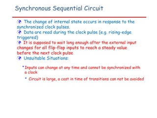
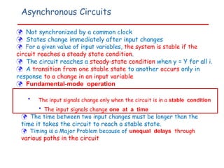
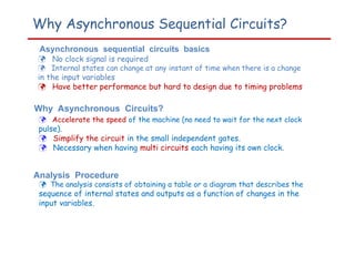
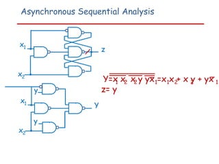
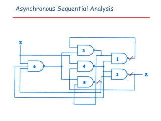
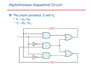
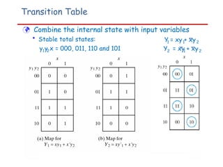
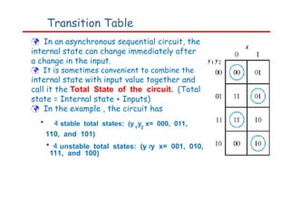
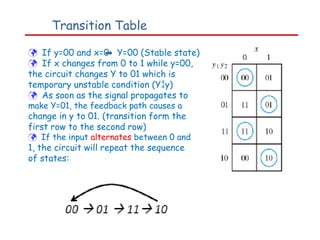
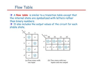
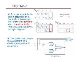
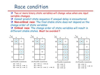
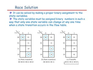
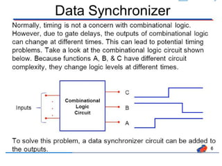
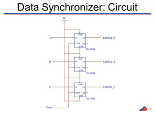
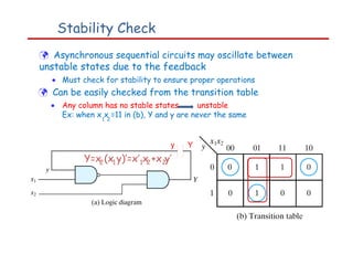
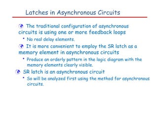
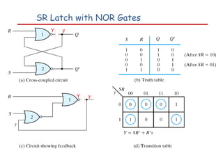
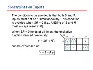
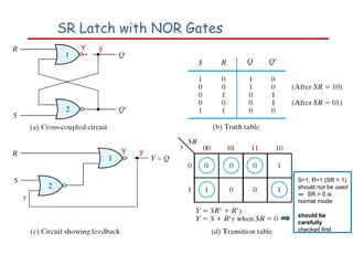
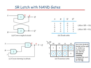
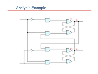
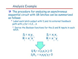
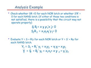
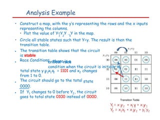
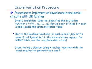
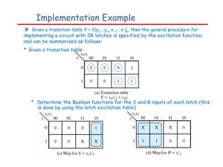
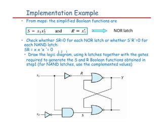
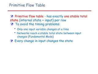
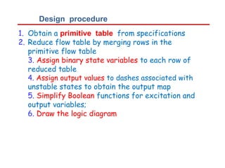
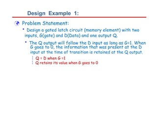
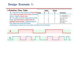
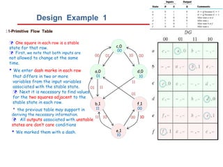
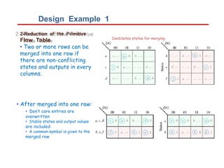
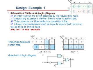
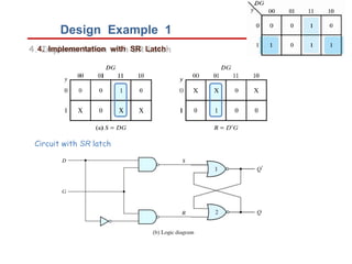
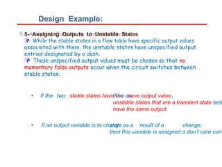
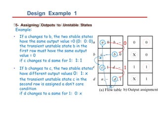
UNIT –II
Asynchronous Sequential
Logic
By,
t.KESAVAN, AP/EEE
Synchronous Sequential Circuit
 The change of internal state occurs in response to the
synchronized clock pulses.
 Data are read during the clock pulse (e.g. rising-edge
triggered)
 It is supposed to wait long enough after the external input
changes for all flip-flop inputs to reach a steady value
before the next clock pulse
 Unsuitable Situations:
•Inputs can change at any time and cannot be synchronized with
a clock
• Circuit is large, a cost in time of transitions can not be avoided
Asynchronous Circuits
 Not synchronized by a common clock
 States change immediately after input changes
 For a given value of input variables, the system is stable if the
circuit reaches a steady state condition.
 The circuit reaches a steady‐state condition when y = Y for all i.
 A transition from one stable state to another occurs only in
response to a change in an input variable
 Fundamental mode operation
‐
i i
• The input signals change only when the circuit is in a stable condition
• The input signals change one at a time
 The time between two input changes must be longer than the
time it takes the circuit to reach a stable state.
 Timing is a Major Problem because of unequal delays through
various paths in the circuit
Why Asynchronous Sequential Circuits?
Asynchronous sequential circuits basics
 No clock signal is required
 Internal states can change at any instant of time when there is a change
in the input variables
 Have better performance but hard to design due to timing problems
Why Asynchronous Circuits?
 Accelerate the speed of the machine (no need to wait for the next clock
pulse).
 Simplify the circuit in the small independent gates.
 Necessary when having multi circuits each having its own clock.
Analysis Procedure
 The analysis consists of obtaining a table or a diagram that describes the
sequence of internal states and outputs as a function of changes in the
input variables.
Example Circuit
 First construction of
Asynchronous Circuits:
• using only gates
• with feedback paths
 Analysis:
• Lump all of the delay associated
with each feedback path into a
“delay” box
• Associate a state variable with
each delay output
• Construct the flow table
 Network equations
Q
Q
1
+ = X X ’+ X ’X Q +X Q Q ’
1 2 1 2 2 2 1 2
2
+ = X ’X Q ’+ X Q + X Q
1 2 1 1 2 2 2
Z = X  Q  Q
1 1 2
Example Circuit: Output Table
 1. Starting in total state
X X Q Q =0000
1 2 1 2
 2. Input changes to 01
• Internal state changes to 01 and then
to 11.
 3. Input changes to 11.
• Go to unstable total state 1111 and
then to 1101.
 4. Input changes to 10.
• Go to unstable total state 1001 and
then to 1011.
 The output sequence:
0 (0) (1) 0 (1) 0
(0) 1
• Condensed to the form
0 (1) 0 (1) 0 1.
• Two transient 1 outputs is dangerous
can be eliminated by proper design.
Q
Q
1
+ = X X ’+ X ’X Q +X Q Q ’
1 2 1 2 2 2 1 2
2
+ = X ’X Q ’+ X Q + X Q
1 2 1 1 2 2 2
Z = X  Q  Q
1 1 2
Transition Table
 Transition table is useful to analyze an asynchronous circuit
from the circuit diagram. Procedure to obtain transition table:
1. Determine all feedback loops in the circuits
2. Mark the input (y ) and output (Y ) of each feedback loop
i i
3. Derive the Boolean functions of all Y’s
4. Plot each Y function in a map and combine all maps into one table (flow
table)
5. Circle those values of Y in each square that are equal to the value of y in
the same row (stable states)
Asynchronous Sequential Analysis
x1
x2
z
Y=x x x y =x x + x y
1 2 2 1 2 2
z= Y
x1
x2
z
Y
y
Asynchronous Sequential Analysis
x1
x2
z
Y=x x x y yx =x x + x y + yx
1 2 2 1 1 2 2 1
z= y
x1
x2
Y
y
y
Asynchronous Sequential Analysis
Asynchronous Sequential Circuit
 The state variables: Y and Y
1 2
• Y1 = xy + xy
1 2
• Y = xy + xy
2 1 2
CUT
CUT
Transition Table
 Combine the internal state with input variables
• Stable total states:
y y x = 000, 011, 110 and 101
1 2
Y = xy + xy
1 1 2
Y2 = xy + xy
1 2
Transition Table
 In an asynchronous sequential circuit, the
internal state can change immediately after
a change in the input.
 It is sometimes convenient to combine the
internal state with input value together and
call it the Total State of the circuit. (Total
state = Internal state + Inputs)
 In the example , the circuit has
• 4 stable total states: (y y x= 000, 011,
1 2
110, and 101)
• 4 unstable total states: (y y x= 001, 010,
1 2
111, and 100)
Transition Table
 If y=00 and x=0 Y=00 (Stable state)
 If x changes from 0 to 1 while y=00,
the circuit changes Y to 01 which is
temporary unstable condition (Yy)
 As soon as the signal propagates to
make Y=01, the feedback path causes a
change in y to 01. (transition form the
first row to the second row)
 If the input alternates between 0 and
1, the circuit will repeat the sequence
of states:
Flow Table
 A flow table is similar to a transition table except that
the internal state are symbolized with letters rather
than binary numbers.
 It also includes the output values of the circuit for each
stable state.
Flow Table
 In order to obtain the
circuit described by a
flow table, it is necessary
to convert the flow table
into a transition table
from which we can derive
the logic diagram.
 This can be done through
the assignment of a
distinct binary value to
each state.
Assignements:
A≡0 B≡1
Race condition
 Two or more binary state variables will change value when one input
variable changes.
 Cannot predict state sequence if unequal delay is encountered.
 Non-critical race: The final stable state does not depend on the
change order of state variables
 Critical race: The change order of state variables will result in
different stable states. Must be avoided !!
Race Solution
 It can be solved by making a proper binary assignment to the
state variables.
 The state variables must be assigned binary numbers in such a
way that only one state variable can change at any one time
when a state transition occurs in the flow table.
Stability Check
 Asynchronous sequential circuits may oscillate between
unstable states due to the feedback
• Must check for stability to ensure proper operations
 Can be easily checked from the transition table
• Any column has no stable states unstable
Ex: when x x =11 in (b), Y and y are never the same
1 2
y Y
Y=x (x y)’=x’ x +x y’
2 1 1 2 2
Latches in Asynchronous Circuits
 The traditional configuration of asynchronous
circuits is using one or more feedback loops
• No real delay elements.
 It is more convenient to employ the SR latch as a
memory element in asynchronous circuits
• Produce an orderly pattern in the logic diagram with the
memory elements clearly visible.
 SR latch is an asynchronous circuit
• So will be analyzed first using the method for asynchronous
circuits.
SR Latch with NOR Gates
Y y
Y y
Constraints on Inputs
-
-
SR Latch with NOR Gates
S=1, R=1 (SR = 1)
should not be used
⇒ SR = 0 is
normal mode
should be
carefully
checked first
Y y
Y y
SR Latch with NAND Gates
S=0, R=0 (S+R=0)
should not be used
⇒ S+R=1 is
normal mode
(eq. S’R’=0)
should be
carefully
checked first, so it
is obtained
Y = S’ + Ry
Y y
Y y
Analysis Example
Y1 y1
Y2 y2
Analysis Example
 The procedure for analyzing an asynchronous
sequential circuit with SR latches can be summarized
as follows:
• Label each latch output with Y and its external feedback
i
path with y for i=1,2,…,k
• Derive the Boolean functions for the S and R inputs in each
i
i i
latch.
S = x y
R = x ‘x ‘
1 1 2
S = x x
R = x ‘ y
2 1 2
1 1 2 2 2 1
S R = x y x ‘x ‘= 0
1 1 1 2 1 2
S R
2 2 = x x x ‘y = 0
1 2 2 1
Analysis Example
• Check whether SR =0 for each NOR latch or whether S’R’ =
0 for each NAND latch. (if either of these two conditions is
not satisfied, there is a possibility that the circuit may not
operate properly)
S R = x y x ‘x ‘= 0
1 1 1 2 1 2
S R
2 2 = x x x ‘y = 0
1 2 2 1
• Evaluate Y = S + R’y for each NOR latch or Y = S’ + Ry for
each NAND latch.
Y1 = S1 + R ‘ y
1 1 = x y
1 2 + x y + x y
1 1 2 1
Y = S + R ‘ y = x x + x y
2 2 2 2 1 2 2 2 + y ’y
1 2
Analysis Example
• Construct a map, with the y’s representing the rows and the x inputs
representing the columns.
• Plot the value of Y=Y Y …Y in the map.
1 2 k
• Circle all stable states such that Y=y. The result is then the
transition table.
Transition Table
• The transition table shows that the circuit
is stable
Race Conditions:
• there is a
critical race
condition when the circuit is initially in
total state y y x x
1 2 1 2 = 1101 and x2 changes
from 1 to 0.
The circuit should go to the total
• state
0000.
• If Y1 changes to 0 before Y2, the circuit
goes to total state 0100 instead of 0000.
Y = x y
1 1 2 + x y + x y
1 1 2 1
Y = x x + x y
2 1 2 2 2 + y ’y
1 2
Implementation Procedure
 Procedure to implement an asynchronous sequential
circuits with SR latches:
• Given a transition table that specifies the excitation
function Y = f(y ,-,y , x ,-, x ) derive a pair of maps for each
S and R using the latch excitation table
1 n 1 m
i i
• Derive the Boolean functions for each S and R (do not to
i i
make S and R equal to 1 in the same minterm square; for
NAND latch, use the complemented values)
i i
• Draw the logic diagram using k latches together with the
gates required to generate the S and R
Implementation Example
 Given a transition table Y = f(y ,-,y , x ,-, x ) , then the general procedure for
implementing a circuit with SR latches is specified by the excitation function,
and can be summarized as follows:
• Given a transition table
1 n 1 m
• Determine the Boolean functions for the S and R inputs of each latch (this
is done by using the latch excitation table)
Implementation Example
• From maps: the simplified Boolean functions are
• Check whether SR=0 for each NOR latch or whether S'R'=0 for
each NAND latch:
SR = x x ’x '= 0
• Draw the logic diagram, using k latches together with the gates
1 2 1
required to generate the S and R Boolean functions obtained in
step1 (for NAND latches, use the complemented values)
NOR latch
Primitive Flow Table
 Primitive flow table - has exactly one stable total
state (internal state + input) per row
 To avoid the timing problems:
• Only one input variable changes at a time
• Networks reach a stable total state between input
changes (Fundamental Mode)
 Every change in input changes the state
Design procedure
1.
2.
Obtain a primitive table from specifications
Reduce flow table by merging rows in the
primitive flow table
3. Assign binary state variables to each row of
reduced table
4. Assign output values to dashes associated with
unstable states to obtain the output map
5. Simplify Boolean functions for excitation and
output variables;
6. Draw the logic diagram
Design Example 1:
 Problem Statement:
• Design a gated latch circuit (memory element) with two
inputs, G(gate) and D(Data) and one output Q.
• The Q output will follow the D input as long as G=1. When
G goes to 0, the information that was present at the D
input at the time of transition is retained at the Q output.
 Q = D when G =1
 Q retains its value when G goes to 0
Design Example 1:
1-Primitive Flow Table
 A primitive flow table is a flow table
with only one stable total state (internal
state + input) in each row.
 In order to form the primitive flow
table, we first form a table with all
possible total states, combinations of
the inputs and internal states,
simultaneous transitions of two input variables are not allowed
c d b a b a c d c a b a b e f e f
G
D
Q
Design Example 1
1-Primitive Flow Table
 One square in each row is a stable
state for that row.
 First, we note that both inputs are
not allowed to change at the same
time.
• We enter dash marks in each row
that differs in two or more
variables from the input variables
associated with the stable state.
 Next it is necessary to find values
for the two squares adjacent to the
stable state in each row.
• the previous table may support in
deriving the necessary information.
 All outputs associated with unstable
states are don’t care conditions
• We marked them with a dash.
c,0
d,0
a,0
f,1
b,1
e,1
00 10
01
11
00
11
01 10
01
10
10
00
11
10
00
01
00
11
Design Example 1
2-Reduction of the Primitive
Flow Table
• Two or more rows can be
merged into one row if
there are non-conflicting
states and outputs in every
columns.
• After merged into one row:
• Don’t care entries are
overwritten
• Stable states and output values
are included
• A common symbol is given to the
merged row
Candidates states for merging:
Design Example 1
3-Transition Table and Logic Diagram
 In order to obtain the circuit described by the reduced flow table,
it is necessary to assign a distinct binary value to each state.
 This converts the flow table to a transition table.
 A binary state assignment must be made to ensure that the circuit
will be free of critical race.
a=0, b=1 in this example
Transition table and
output map
Gated-latch logic diagram
Design Example 1
4. Implementation with SR Latch
Circuit with SR latch
Design Example:
5- Assigning Outputs to Unstable States
 While the stable states in a flow table have specific output values
associated with them, the unstable states have unspecified output
entries designated by a dash.
 These unspecified output values must be chosen so that no
momentary false outputs occur when the circuit switches between
stable states.
• If the two stable states have the save output value,
then an
unstable states that are a transient state betw
have the same output.
• If an output variable is to change as a result of a
state
then this variable is assigned a don’t care cond
change,
Design Example 1
5- Assigning Outputs to Unstable States
Example:
• If a changes to b, the two stable states
have the same output value =0 (00: 0)
the transient unstable state b in the
first row must have the same output
value = 0
if c changes to d same for 11: 1
• If b changes to c, the two stable states
have different output values 01: x
the transient unstable state c in the
second row is assigned a don’t care
condition
if d changes to a same for 10: x
0
1
x
x

DPSD-Asynchronous-sequential-circuits.ppt

  • 1.
  • 2.
    Synchronous Sequential Circuit The change of internal state occurs in response to the synchronized clock pulses.  Data are read during the clock pulse (e.g. rising-edge triggered)  It is supposed to wait long enough after the external input changes for all flip-flop inputs to reach a steady value before the next clock pulse  Unsuitable Situations: •Inputs can change at any time and cannot be synchronized with a clock • Circuit is large, a cost in time of transitions can not be avoided
  • 3.
    Asynchronous Circuits  Notsynchronized by a common clock  States change immediately after input changes  For a given value of input variables, the system is stable if the circuit reaches a steady state condition.  The circuit reaches a steady‐state condition when y = Y for all i.  A transition from one stable state to another occurs only in response to a change in an input variable  Fundamental mode operation ‐ i i • The input signals change only when the circuit is in a stable condition • The input signals change one at a time  The time between two input changes must be longer than the time it takes the circuit to reach a stable state.  Timing is a Major Problem because of unequal delays through various paths in the circuit
  • 4.
    Why Asynchronous SequentialCircuits? Asynchronous sequential circuits basics  No clock signal is required  Internal states can change at any instant of time when there is a change in the input variables  Have better performance but hard to design due to timing problems Why Asynchronous Circuits?  Accelerate the speed of the machine (no need to wait for the next clock pulse).  Simplify the circuit in the small independent gates.  Necessary when having multi circuits each having its own clock. Analysis Procedure  The analysis consists of obtaining a table or a diagram that describes the sequence of internal states and outputs as a function of changes in the input variables.
  • 5.
    Example Circuit  Firstconstruction of Asynchronous Circuits: • using only gates • with feedback paths  Analysis: • Lump all of the delay associated with each feedback path into a “delay” box • Associate a state variable with each delay output • Construct the flow table  Network equations Q Q 1 + = X X ’+ X ’X Q +X Q Q ’ 1 2 1 2 2 2 1 2 2 + = X ’X Q ’+ X Q + X Q 1 2 1 1 2 2 2 Z = X  Q  Q 1 1 2
  • 6.
    Example Circuit: OutputTable  1. Starting in total state X X Q Q =0000 1 2 1 2  2. Input changes to 01 • Internal state changes to 01 and then to 11.  3. Input changes to 11. • Go to unstable total state 1111 and then to 1101.  4. Input changes to 10. • Go to unstable total state 1001 and then to 1011.  The output sequence: 0 (0) (1) 0 (1) 0 (0) 1 • Condensed to the form 0 (1) 0 (1) 0 1. • Two transient 1 outputs is dangerous can be eliminated by proper design. Q Q 1 + = X X ’+ X ’X Q +X Q Q ’ 1 2 1 2 2 2 1 2 2 + = X ’X Q ’+ X Q + X Q 1 2 1 1 2 2 2 Z = X  Q  Q 1 1 2
  • 7.
    Transition Table  Transitiontable is useful to analyze an asynchronous circuit from the circuit diagram. Procedure to obtain transition table: 1. Determine all feedback loops in the circuits 2. Mark the input (y ) and output (Y ) of each feedback loop i i 3. Derive the Boolean functions of all Y’s 4. Plot each Y function in a map and combine all maps into one table (flow table) 5. Circle those values of Y in each square that are equal to the value of y in the same row (stable states)
  • 8.
    Asynchronous Sequential Analysis x1 x2 z Y=xx x y =x x + x y 1 2 2 1 2 2 z= Y x1 x2 z Y y
  • 9.
    Asynchronous Sequential Analysis x1 x2 z Y=xx x y yx =x x + x y + yx 1 2 2 1 1 2 2 1 z= y x1 x2 Y y y
  • 10.
  • 11.
    Asynchronous Sequential Circuit The state variables: Y and Y 1 2 • Y1 = xy + xy 1 2 • Y = xy + xy 2 1 2 CUT CUT
  • 12.
    Transition Table  Combinethe internal state with input variables • Stable total states: y y x = 000, 011, 110 and 101 1 2 Y = xy + xy 1 1 2 Y2 = xy + xy 1 2
  • 13.
    Transition Table  Inan asynchronous sequential circuit, the internal state can change immediately after a change in the input.  It is sometimes convenient to combine the internal state with input value together and call it the Total State of the circuit. (Total state = Internal state + Inputs)  In the example , the circuit has • 4 stable total states: (y y x= 000, 011, 1 2 110, and 101) • 4 unstable total states: (y y x= 001, 010, 1 2 111, and 100)
  • 14.
    Transition Table  Ify=00 and x=0 Y=00 (Stable state)  If x changes from 0 to 1 while y=00, the circuit changes Y to 01 which is temporary unstable condition (Yy)  As soon as the signal propagates to make Y=01, the feedback path causes a change in y to 01. (transition form the first row to the second row)  If the input alternates between 0 and 1, the circuit will repeat the sequence of states:
  • 15.
    Flow Table  Aflow table is similar to a transition table except that the internal state are symbolized with letters rather than binary numbers.  It also includes the output values of the circuit for each stable state.
  • 16.
    Flow Table  Inorder to obtain the circuit described by a flow table, it is necessary to convert the flow table into a transition table from which we can derive the logic diagram.  This can be done through the assignment of a distinct binary value to each state. Assignements: A≡0 B≡1
  • 17.
    Race condition  Twoor more binary state variables will change value when one input variable changes.  Cannot predict state sequence if unequal delay is encountered.  Non-critical race: The final stable state does not depend on the change order of state variables  Critical race: The change order of state variables will result in different stable states. Must be avoided !!
  • 18.
    Race Solution  Itcan be solved by making a proper binary assignment to the state variables.  The state variables must be assigned binary numbers in such a way that only one state variable can change at any one time when a state transition occurs in the flow table.
  • 22.
    Stability Check  Asynchronoussequential circuits may oscillate between unstable states due to the feedback • Must check for stability to ensure proper operations  Can be easily checked from the transition table • Any column has no stable states unstable Ex: when x x =11 in (b), Y and y are never the same 1 2 y Y Y=x (x y)’=x’ x +x y’ 2 1 1 2 2
  • 23.
    Latches in AsynchronousCircuits  The traditional configuration of asynchronous circuits is using one or more feedback loops • No real delay elements.  It is more convenient to employ the SR latch as a memory element in asynchronous circuits • Produce an orderly pattern in the logic diagram with the memory elements clearly visible.  SR latch is an asynchronous circuit • So will be analyzed first using the method for asynchronous circuits.
  • 24.
    SR Latch withNOR Gates Y y Y y
  • 25.
  • 26.
    SR Latch withNOR Gates S=1, R=1 (SR = 1) should not be used ⇒ SR = 0 is normal mode should be carefully checked first Y y Y y
  • 27.
    SR Latch withNAND Gates S=0, R=0 (S+R=0) should not be used ⇒ S+R=1 is normal mode (eq. S’R’=0) should be carefully checked first, so it is obtained Y = S’ + Ry Y y Y y
  • 28.
  • 29.
    Analysis Example  Theprocedure for analyzing an asynchronous sequential circuit with SR latches can be summarized as follows: • Label each latch output with Y and its external feedback i path with y for i=1,2,…,k • Derive the Boolean functions for the S and R inputs in each i i i latch. S = x y R = x ‘x ‘ 1 1 2 S = x x R = x ‘ y 2 1 2 1 1 2 2 2 1 S R = x y x ‘x ‘= 0 1 1 1 2 1 2 S R 2 2 = x x x ‘y = 0 1 2 2 1
  • 30.
    Analysis Example • Checkwhether SR =0 for each NOR latch or whether S’R’ = 0 for each NAND latch. (if either of these two conditions is not satisfied, there is a possibility that the circuit may not operate properly) S R = x y x ‘x ‘= 0 1 1 1 2 1 2 S R 2 2 = x x x ‘y = 0 1 2 2 1 • Evaluate Y = S + R’y for each NOR latch or Y = S’ + Ry for each NAND latch. Y1 = S1 + R ‘ y 1 1 = x y 1 2 + x y + x y 1 1 2 1 Y = S + R ‘ y = x x + x y 2 2 2 2 1 2 2 2 + y ’y 1 2
  • 31.
    Analysis Example • Constructa map, with the y’s representing the rows and the x inputs representing the columns. • Plot the value of Y=Y Y …Y in the map. 1 2 k • Circle all stable states such that Y=y. The result is then the transition table. Transition Table • The transition table shows that the circuit is stable Race Conditions: • there is a critical race condition when the circuit is initially in total state y y x x 1 2 1 2 = 1101 and x2 changes from 1 to 0. The circuit should go to the total • state 0000. • If Y1 changes to 0 before Y2, the circuit goes to total state 0100 instead of 0000. Y = x y 1 1 2 + x y + x y 1 1 2 1 Y = x x + x y 2 1 2 2 2 + y ’y 1 2
  • 32.
    Implementation Procedure  Procedureto implement an asynchronous sequential circuits with SR latches: • Given a transition table that specifies the excitation function Y = f(y ,-,y , x ,-, x ) derive a pair of maps for each S and R using the latch excitation table 1 n 1 m i i • Derive the Boolean functions for each S and R (do not to i i make S and R equal to 1 in the same minterm square; for NAND latch, use the complemented values) i i • Draw the logic diagram using k latches together with the gates required to generate the S and R
  • 33.
    Implementation Example  Givena transition table Y = f(y ,-,y , x ,-, x ) , then the general procedure for implementing a circuit with SR latches is specified by the excitation function, and can be summarized as follows: • Given a transition table 1 n 1 m • Determine the Boolean functions for the S and R inputs of each latch (this is done by using the latch excitation table)
  • 34.
    Implementation Example • Frommaps: the simplified Boolean functions are • Check whether SR=0 for each NOR latch or whether S'R'=0 for each NAND latch: SR = x x ’x '= 0 • Draw the logic diagram, using k latches together with the gates 1 2 1 required to generate the S and R Boolean functions obtained in step1 (for NAND latches, use the complemented values) NOR latch
  • 35.
    Primitive Flow Table Primitive flow table - has exactly one stable total state (internal state + input) per row  To avoid the timing problems: • Only one input variable changes at a time • Networks reach a stable total state between input changes (Fundamental Mode)  Every change in input changes the state
  • 36.
    Design procedure 1. 2. Obtain aprimitive table from specifications Reduce flow table by merging rows in the primitive flow table 3. Assign binary state variables to each row of reduced table 4. Assign output values to dashes associated with unstable states to obtain the output map 5. Simplify Boolean functions for excitation and output variables; 6. Draw the logic diagram
  • 37.
    Design Example 1: Problem Statement: • Design a gated latch circuit (memory element) with two inputs, G(gate) and D(Data) and one output Q. • The Q output will follow the D input as long as G=1. When G goes to 0, the information that was present at the D input at the time of transition is retained at the Q output.  Q = D when G =1  Q retains its value when G goes to 0
  • 38.
    Design Example 1: 1-PrimitiveFlow Table  A primitive flow table is a flow table with only one stable total state (internal state + input) in each row.  In order to form the primitive flow table, we first form a table with all possible total states, combinations of the inputs and internal states, simultaneous transitions of two input variables are not allowed c d b a b a c d c a b a b e f e f G D Q
  • 39.
    Design Example 1 1-PrimitiveFlow Table  One square in each row is a stable state for that row.  First, we note that both inputs are not allowed to change at the same time. • We enter dash marks in each row that differs in two or more variables from the input variables associated with the stable state.  Next it is necessary to find values for the two squares adjacent to the stable state in each row. • the previous table may support in deriving the necessary information.  All outputs associated with unstable states are don’t care conditions • We marked them with a dash. c,0 d,0 a,0 f,1 b,1 e,1 00 10 01 11 00 11 01 10 01 10 10 00 11 10 00 01 00 11
  • 40.
    Design Example 1 2-Reductionof the Primitive Flow Table • Two or more rows can be merged into one row if there are non-conflicting states and outputs in every columns. • After merged into one row: • Don’t care entries are overwritten • Stable states and output values are included • A common symbol is given to the merged row Candidates states for merging:
  • 41.
    Design Example 1 3-TransitionTable and Logic Diagram  In order to obtain the circuit described by the reduced flow table, it is necessary to assign a distinct binary value to each state.  This converts the flow table to a transition table.  A binary state assignment must be made to ensure that the circuit will be free of critical race. a=0, b=1 in this example Transition table and output map Gated-latch logic diagram
  • 42.
    Design Example 1 4.Implementation with SR Latch Circuit with SR latch
  • 43.
    Design Example: 5- AssigningOutputs to Unstable States  While the stable states in a flow table have specific output values associated with them, the unstable states have unspecified output entries designated by a dash.  These unspecified output values must be chosen so that no momentary false outputs occur when the circuit switches between stable states. • If the two stable states have the save output value, then an unstable states that are a transient state betw have the same output. • If an output variable is to change as a result of a state then this variable is assigned a don’t care cond change,
  • 44.
    Design Example 1 5-Assigning Outputs to Unstable States Example: • If a changes to b, the two stable states have the same output value =0 (00: 0) the transient unstable state b in the first row must have the same output value = 0 if c changes to d same for 11: 1 • If b changes to c, the two stable states have different output values 01: x the transient unstable state c in the second row is assigned a don’t care condition if d changes to a same for 10: x 0 1 x x