Download to read offline
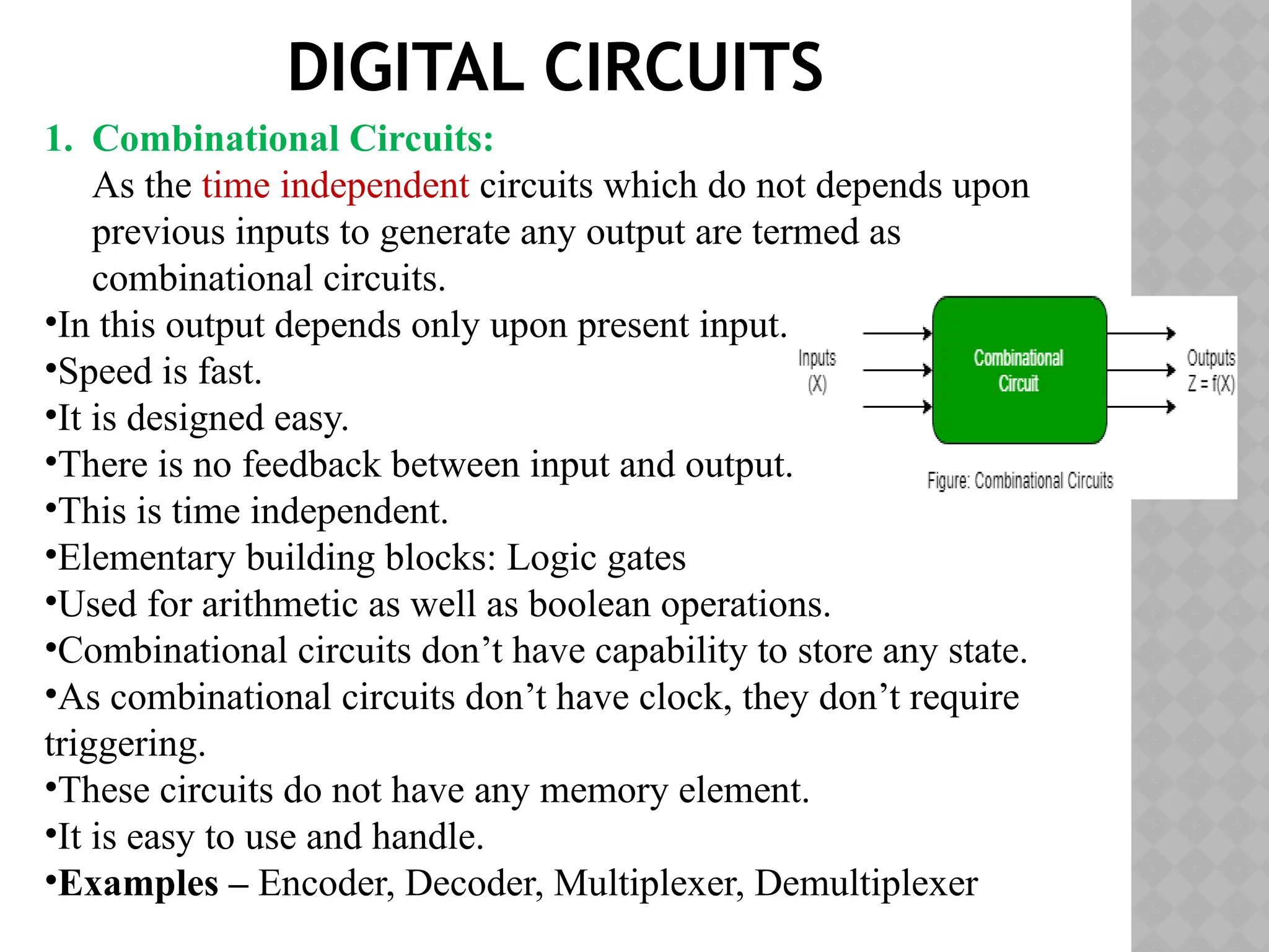
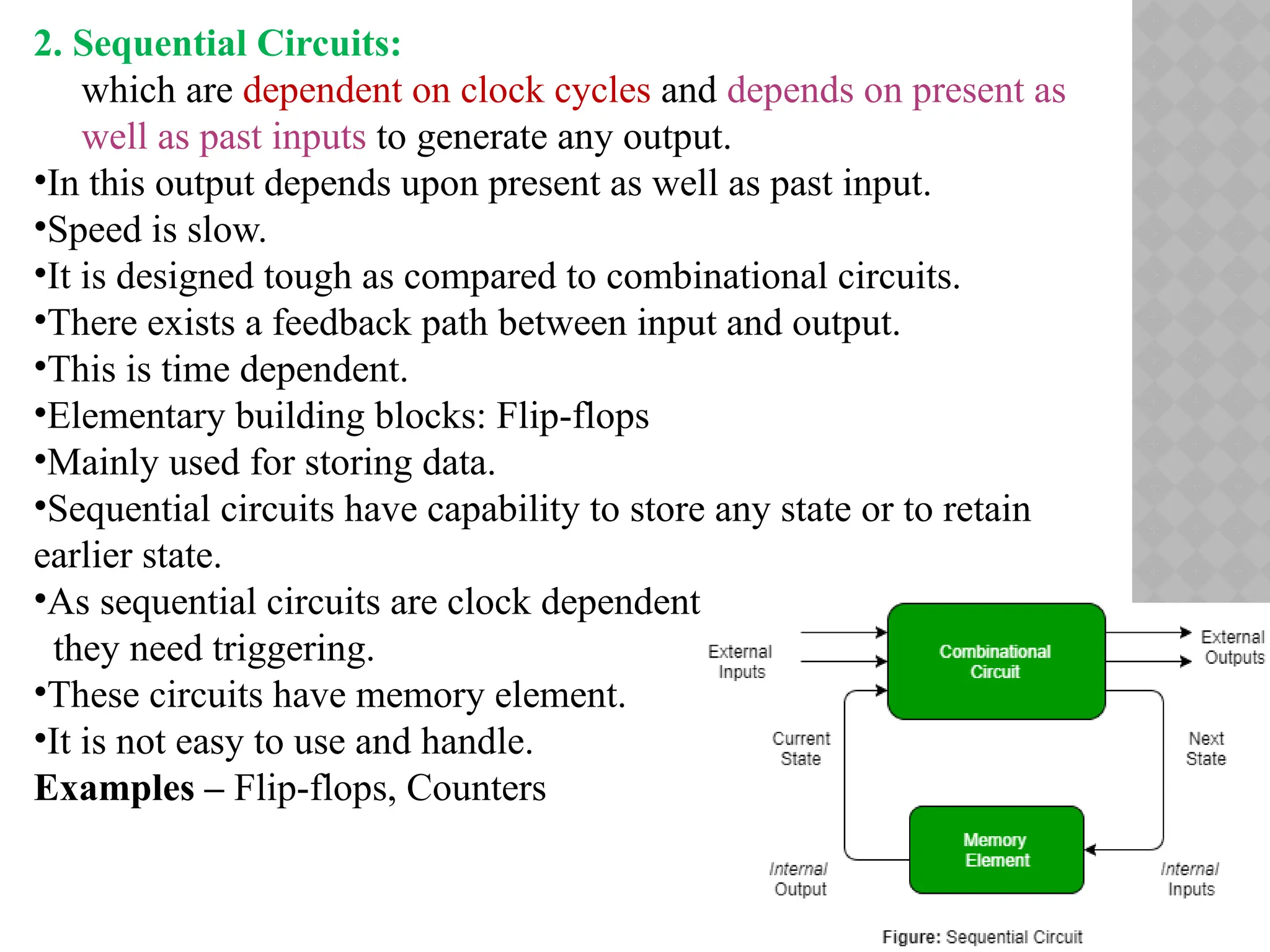

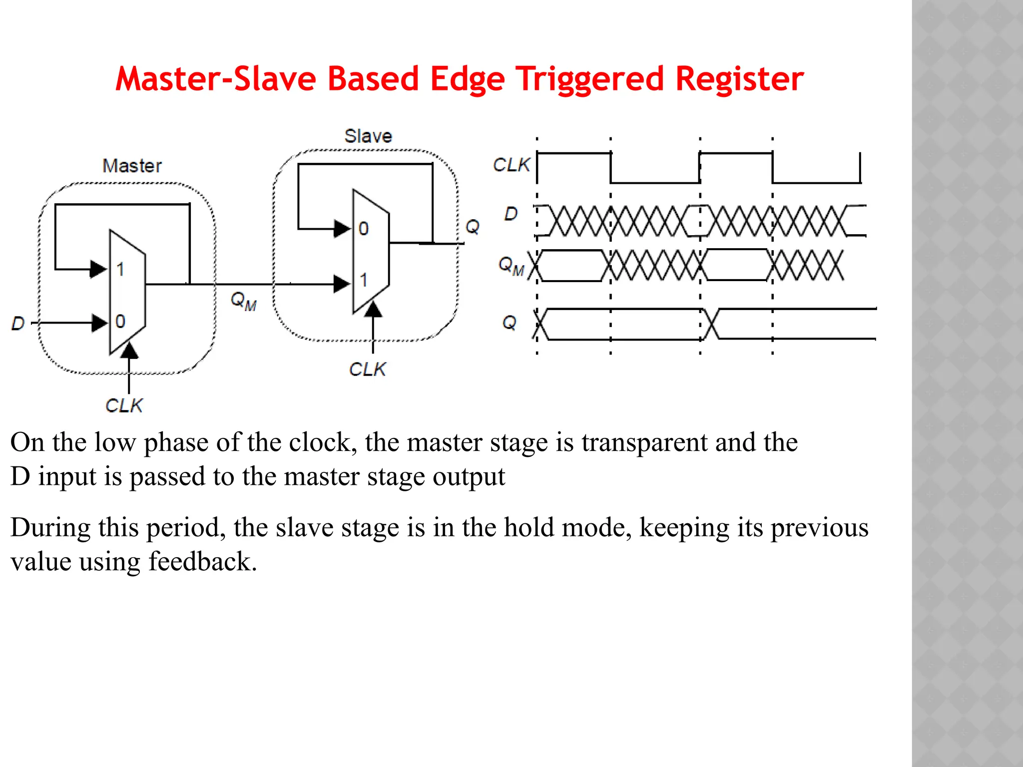
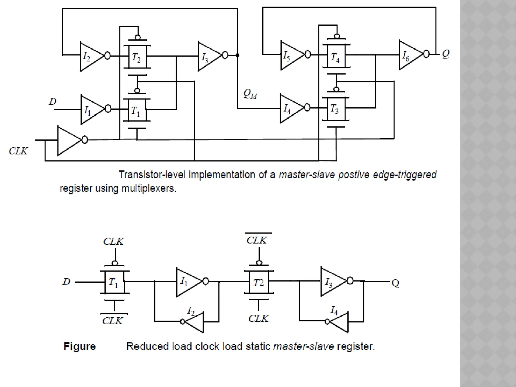
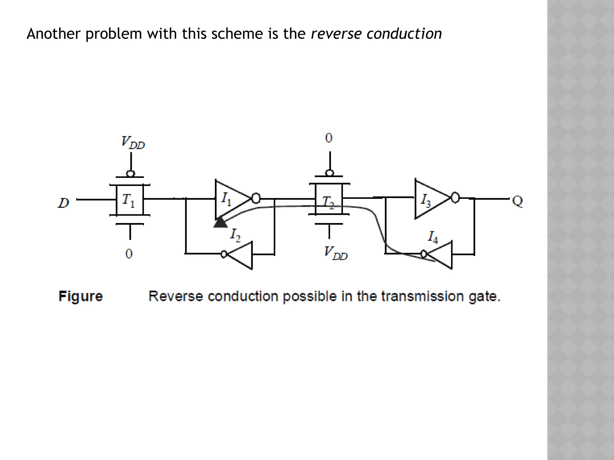
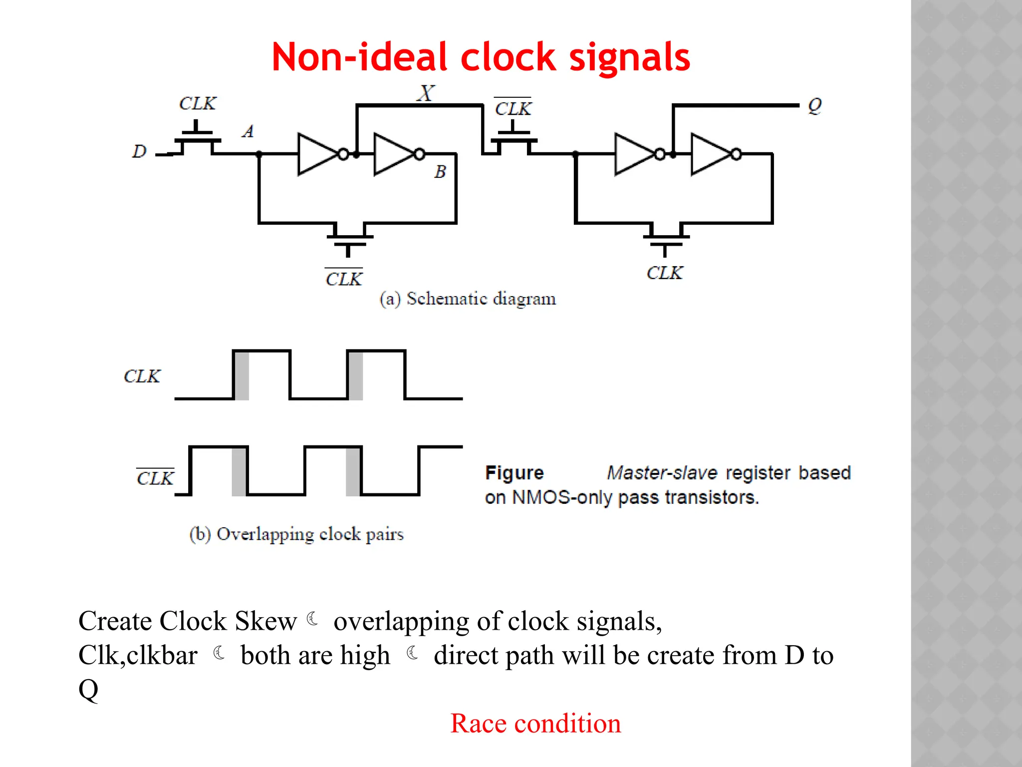
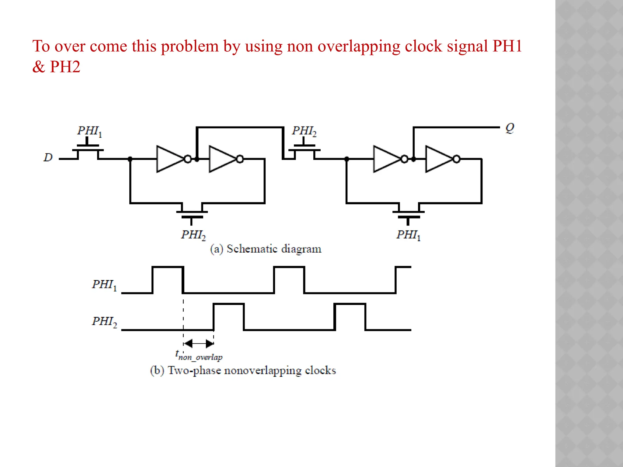
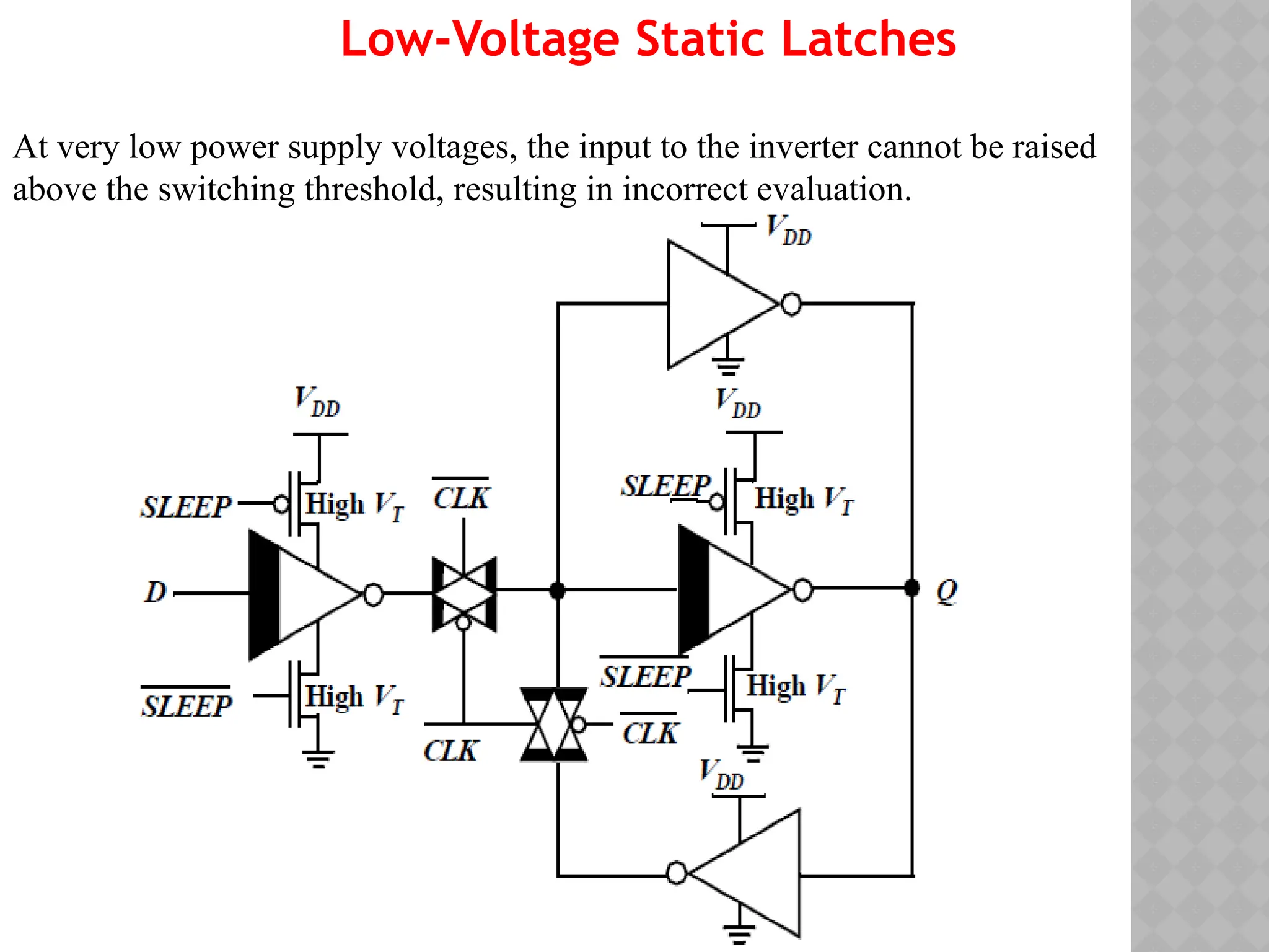

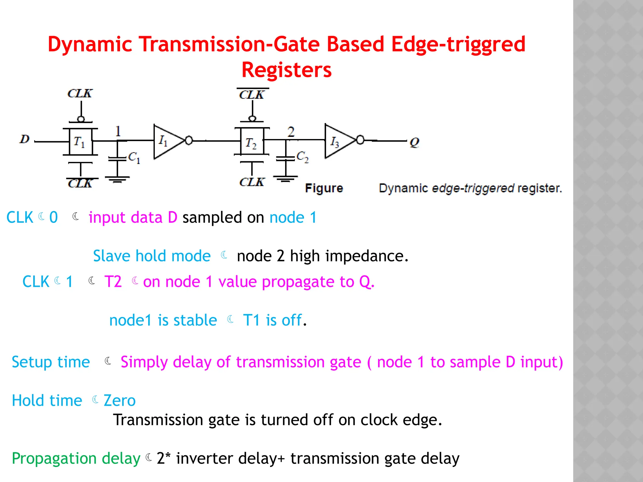
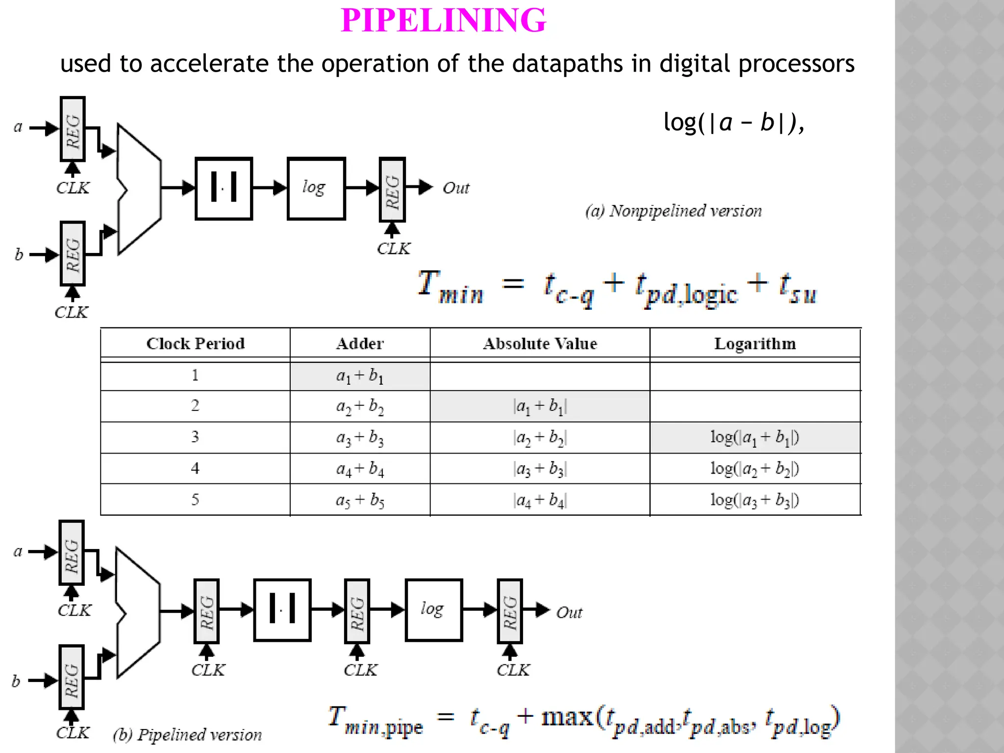
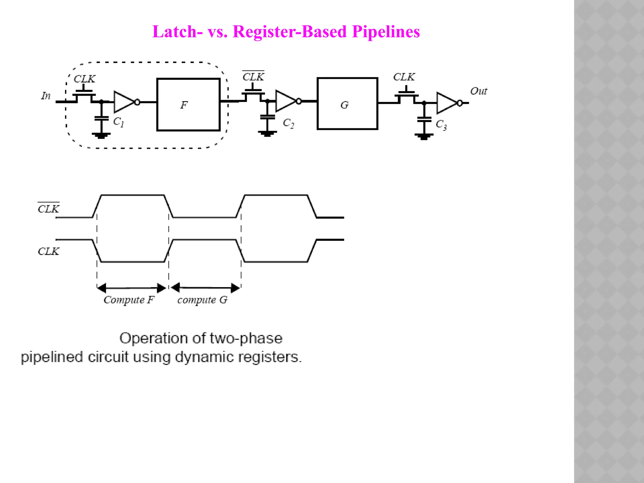
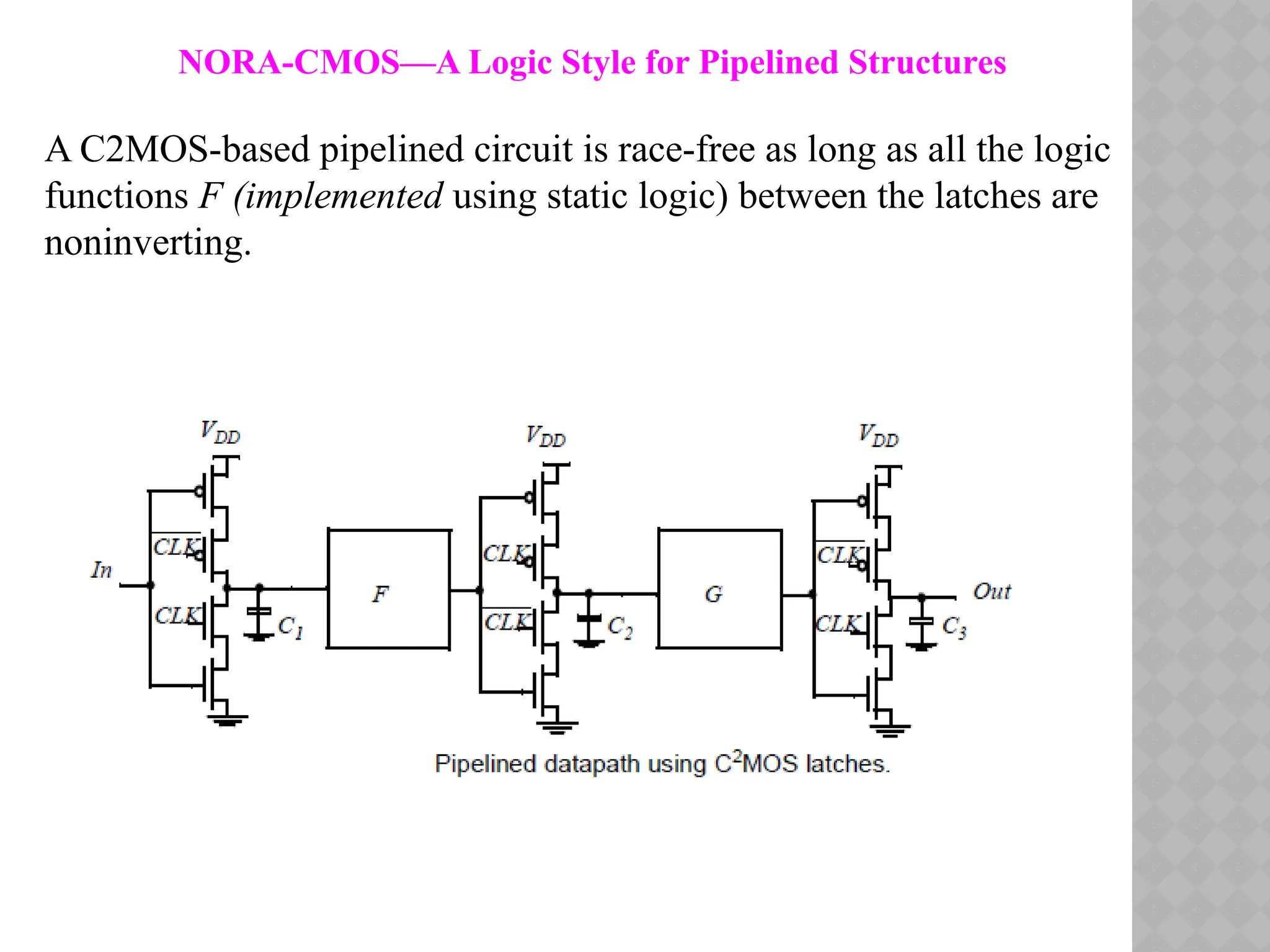
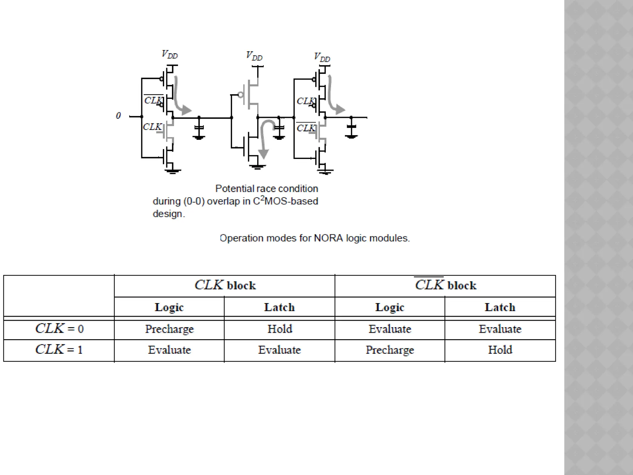
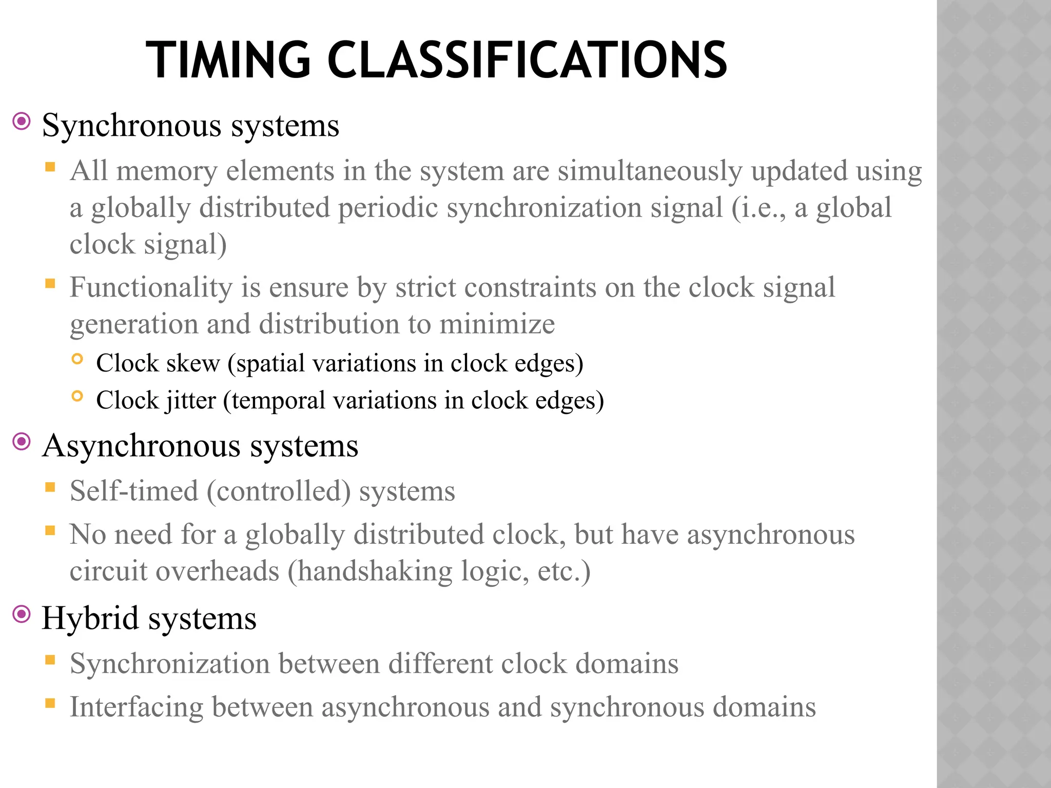
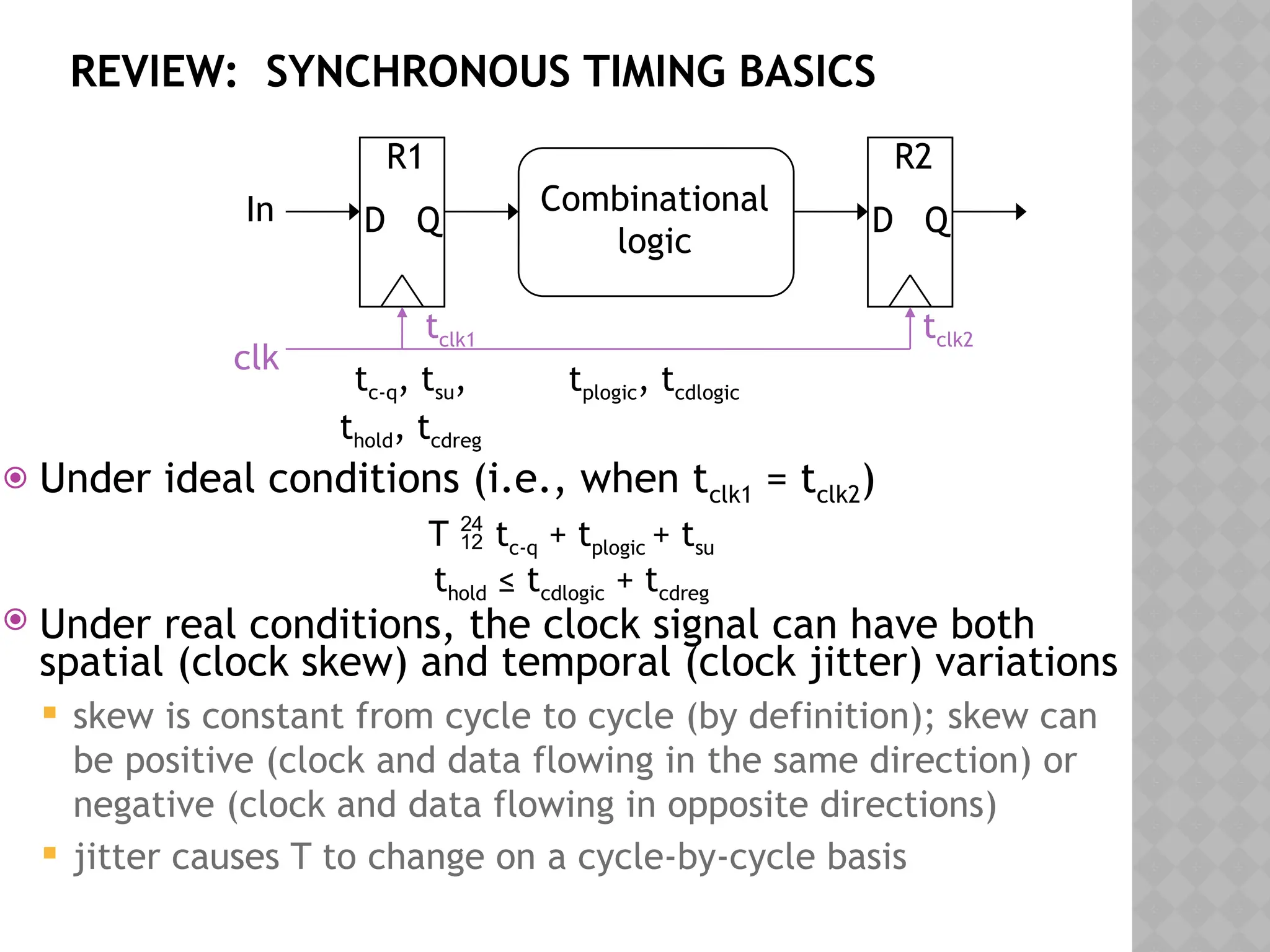
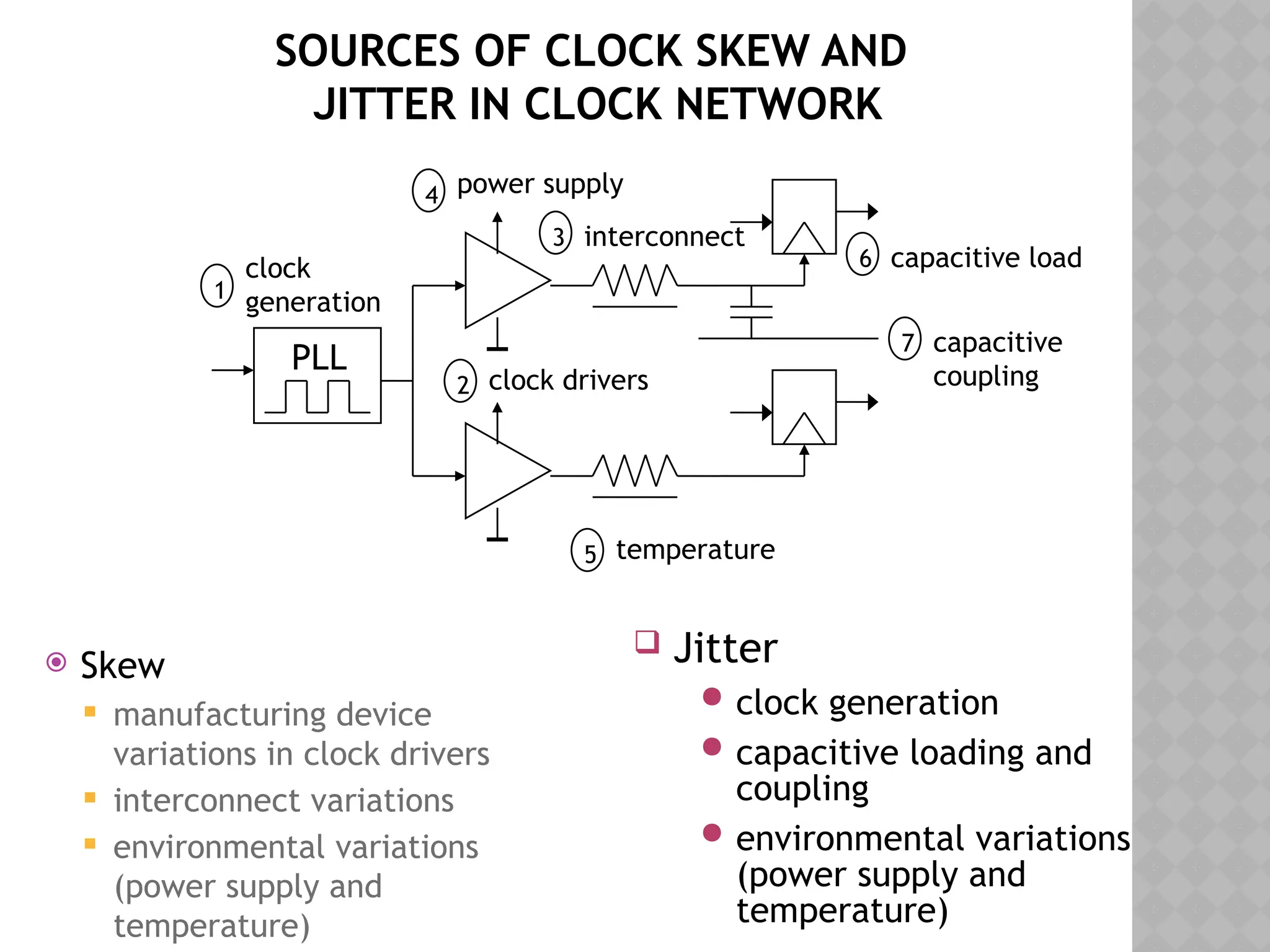
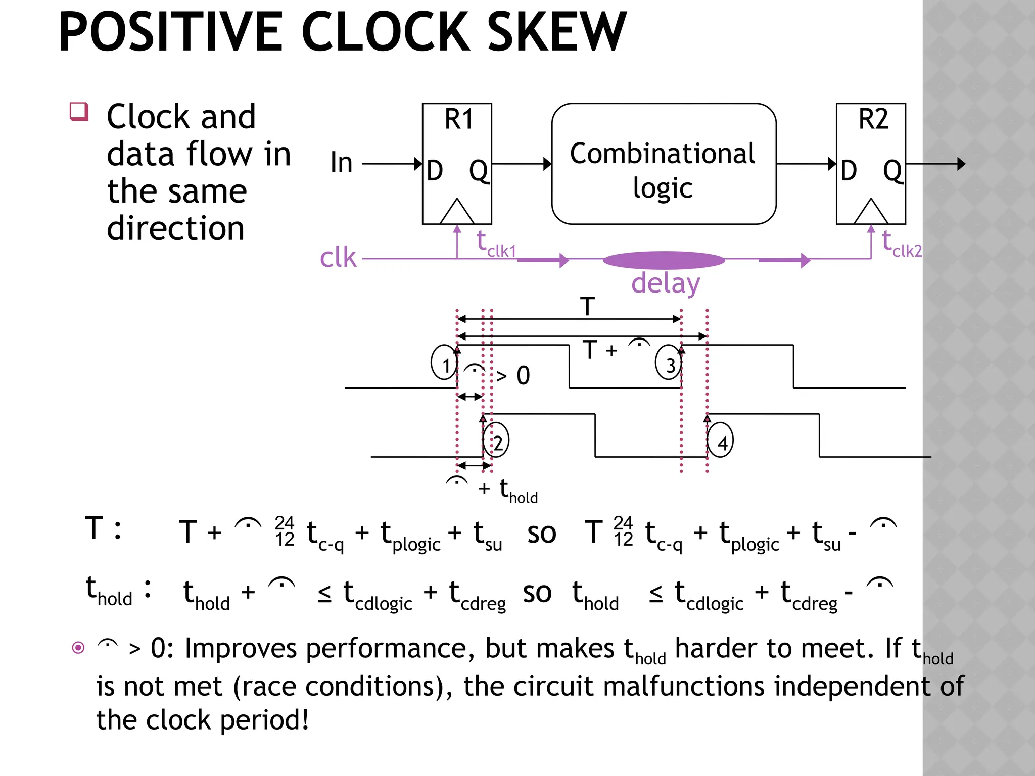
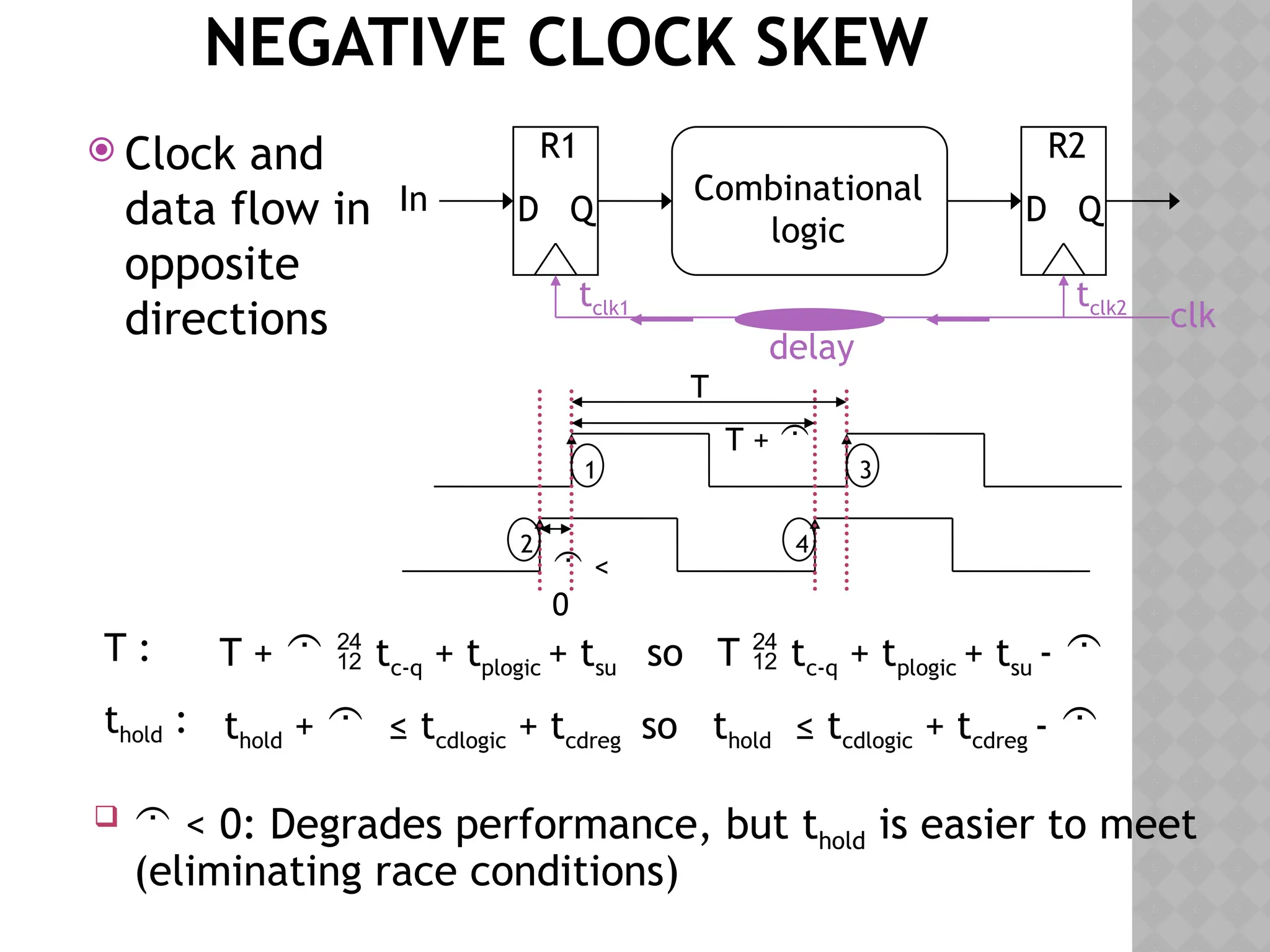
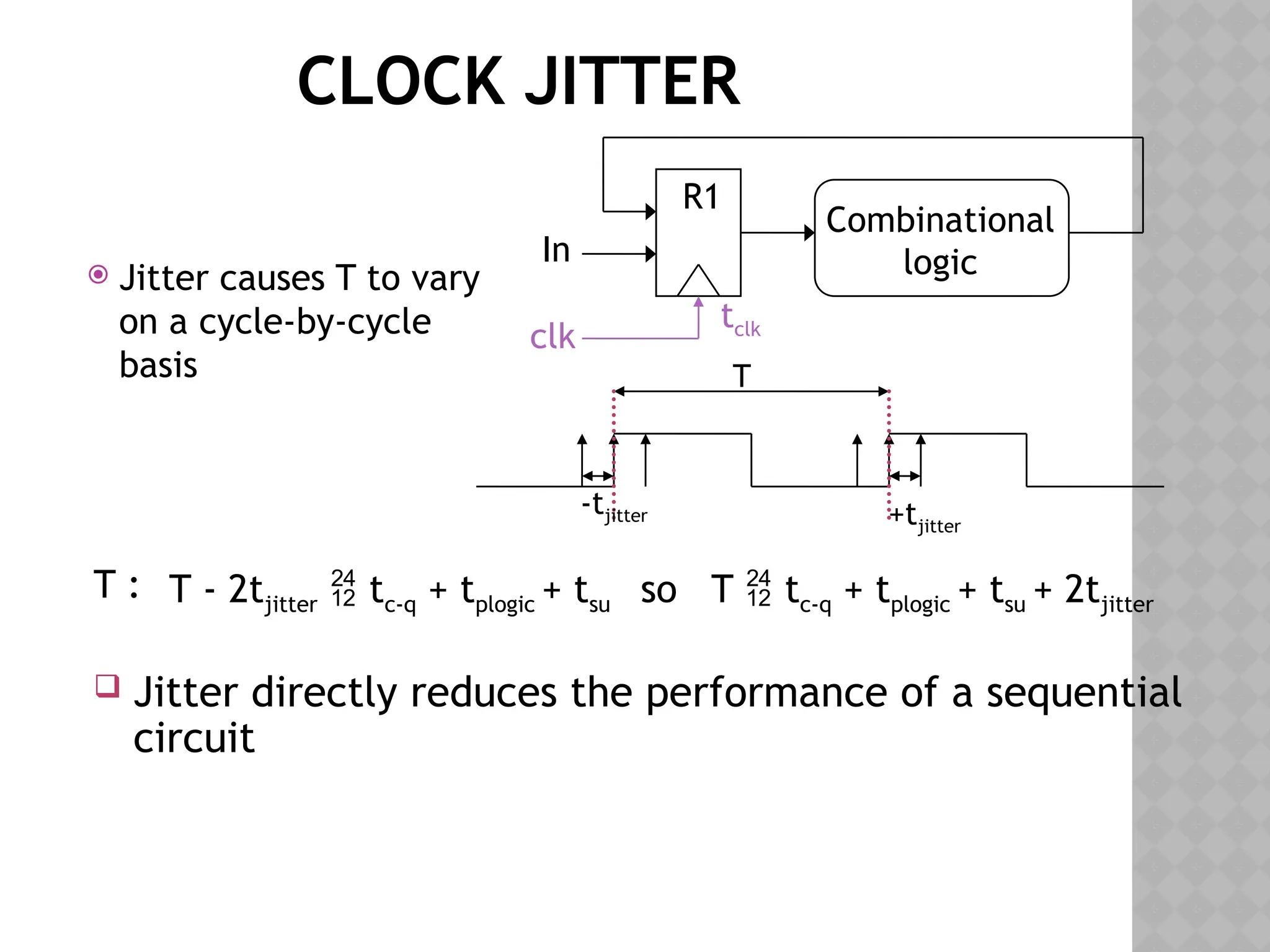
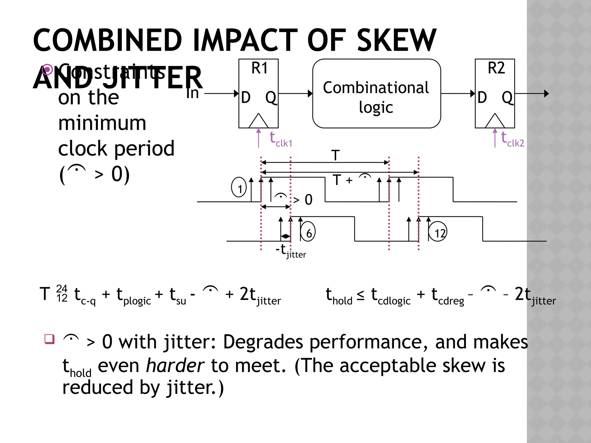
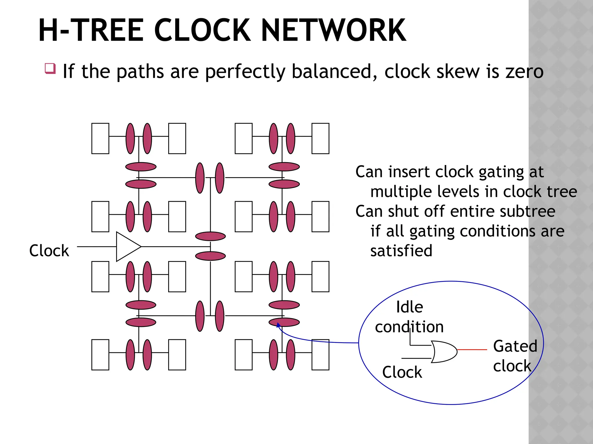
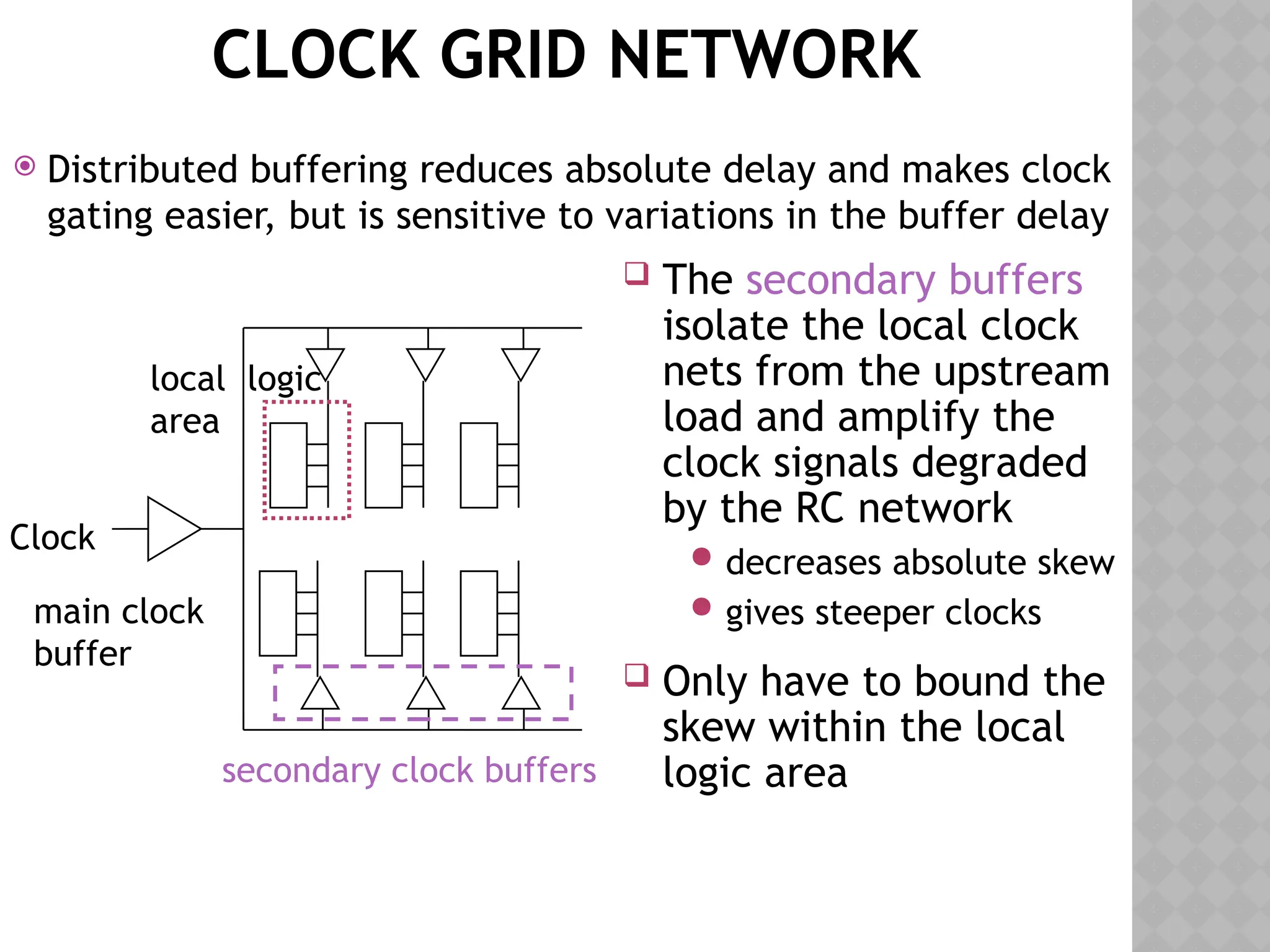

The document discusses the design and functionality of combinational and sequential logic circuits in digital systems. Combinational circuits generate outputs based only on present inputs and do not store states, while sequential circuits rely on clock cycles and past inputs, featuring memory elements. It also highlights various implementations and considerations related to timing, clock skew, and jitter in digital circuit designs.