Downloaded 114 times

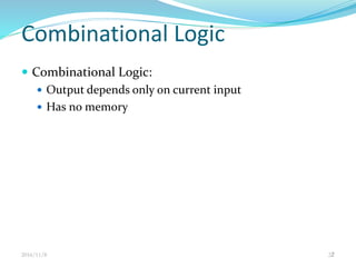
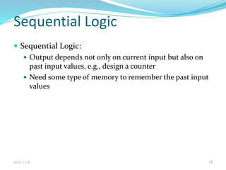
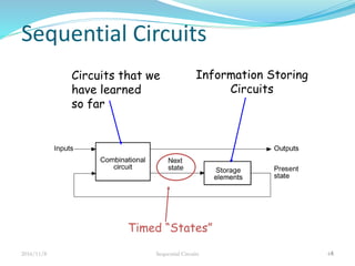
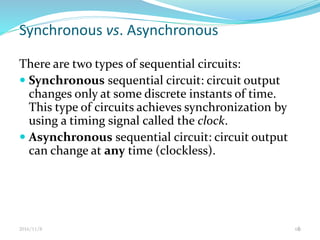
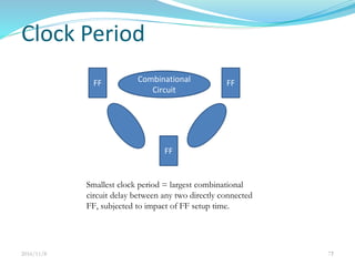
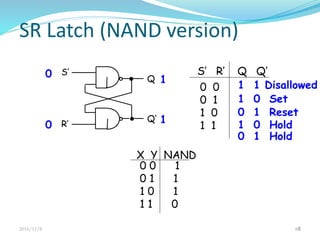
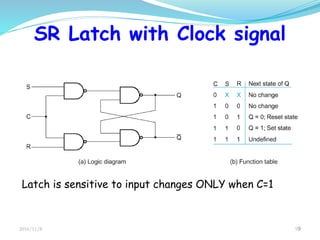
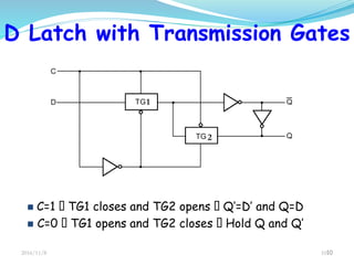
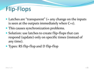
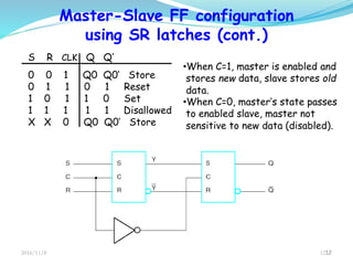
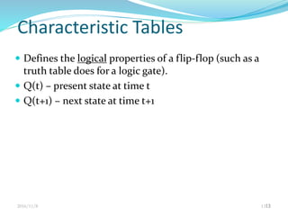
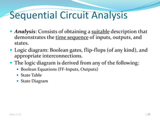
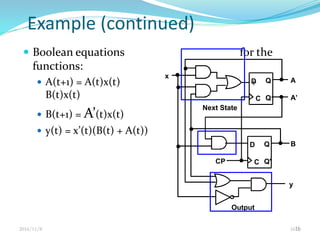
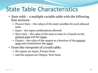


This document discusses sequential circuits and their analysis. It defines sequential logic as circuits whose outputs depend not only on current inputs but also past inputs, requiring some type of memory. There are two types of sequential circuits: synchronous use a clock for synchronization, while asynchronous can change output at any time. Analysis of sequential circuits involves obtaining a description of the input-output-state sequence over time using techniques like logic diagrams, state tables, characteristic tables, and state diagrams. Various flip-flop designs are presented, including the SR latch, D latch using transmission gates, and master-slave flip-flop. Timing considerations like clock period and setup time are also covered.