This document discusses clock distribution networks in integrated circuits. It describes how clock generators produce timing signals to synchronize a system's operation using resonant circuits and amplifiers. As process technologies allow for higher integration and larger die sizes, clock networks must support higher frequencies while minimizing skew and jitter. Various clock distribution topologies are presented, including unconstrained trees, balanced trees, central spines, grids, and hybrid distributions, each with advantages and disadvantages depending on the design.
The clockdistribution network is the metal and buffer
network that distribute clock to all clocked element.
A clock generator is a circuit that produces a timing signal
for use in synchronizing a system’s operation.
At its most basic level, a clock generator consists of a
resonant circuit and an amplifier.
The resonant circuit is usually a quartz piezo-electric
oscillator or MEMS resonator, although simpler tank circuits
and even RC circuits may be used in some cases.
3.
Need tosupport higher clock frequency
based on the strong correlation between
frequency and chip performance.
Process technology scaling allows higher level
of integration and larger die size leading to
higher clock loading and larger distances the
clock network need to traverse.
4.
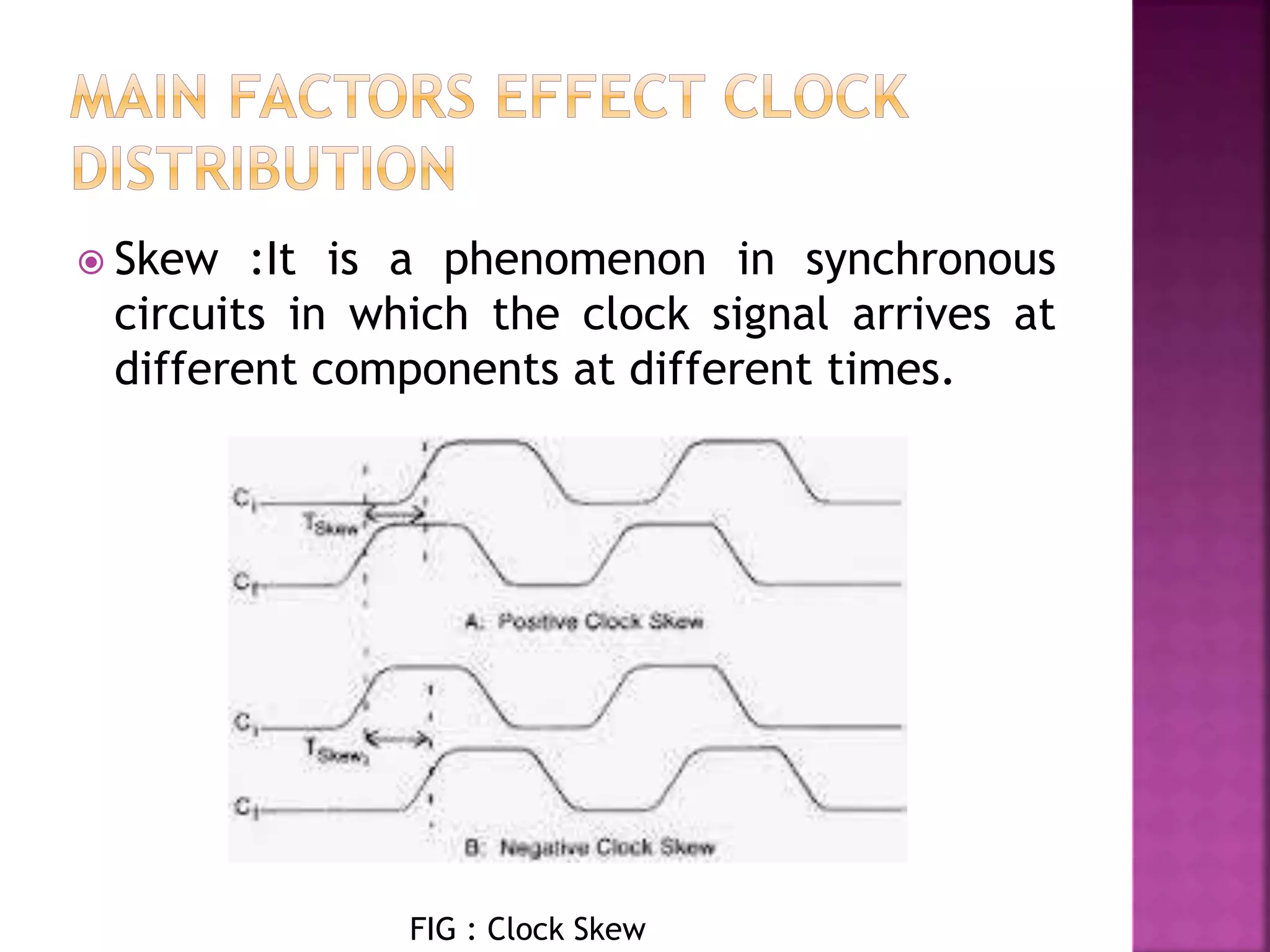
Skew :Itis a phenomenon in synchronous
circuits in which the clock signal arrives at
different components at different times.
FIG : Clock Skew
5.
Clock skewis due to the unbalanced of
the data.
Strategies to remove skew
Locate all clock inputs close together; but it is difficult
to implement in a large circuit.
Drive them from the same source & balance the delays
6.
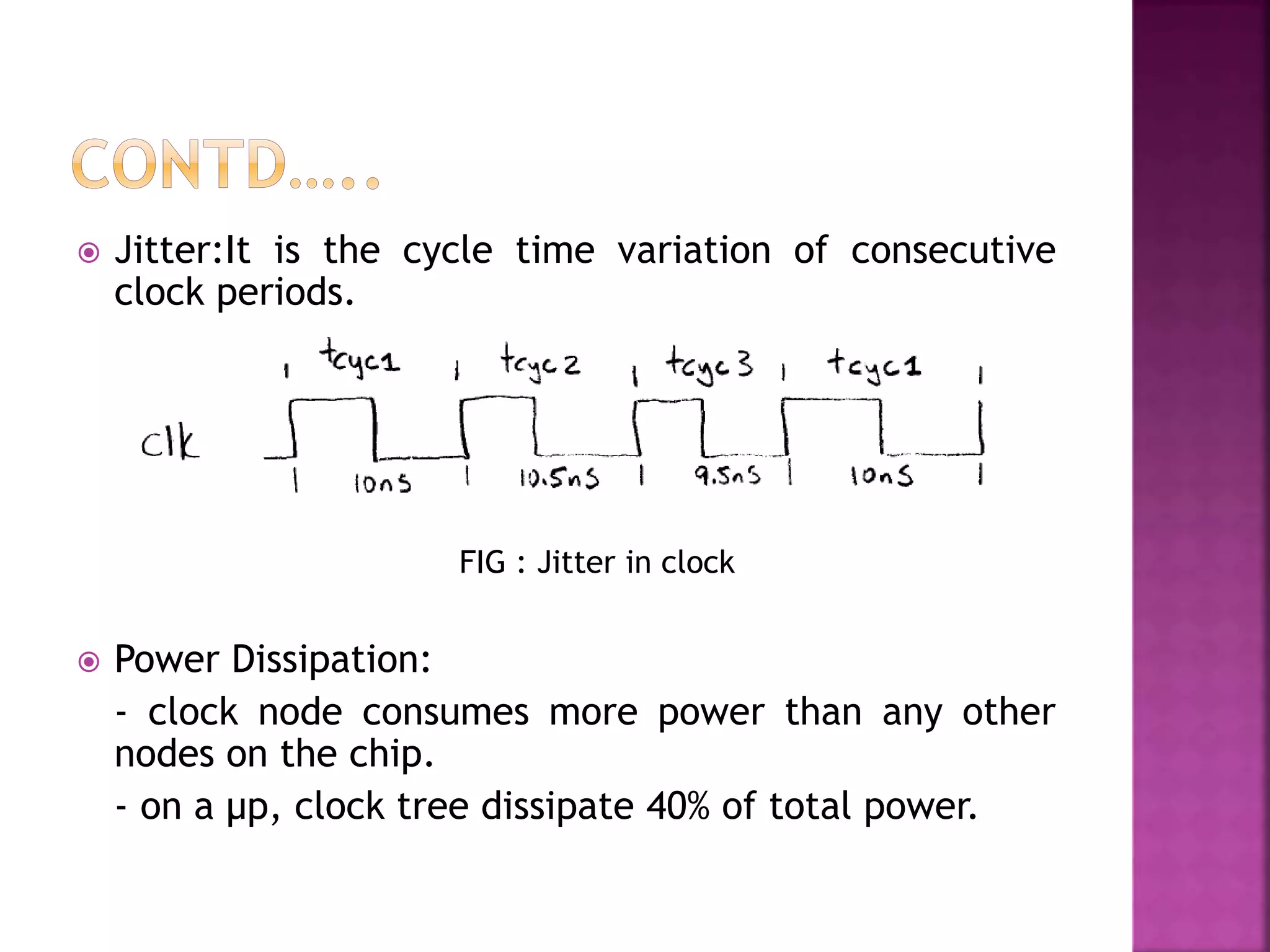
Jitter:It isthe cycle time variation of consecutive
clock periods.
Power Dissipation:
FIG : Jitter in clock
- clock node consumes more power than any other
nodes on the chip.
- on a μp, clock tree dissipate 40% of total power.
7.
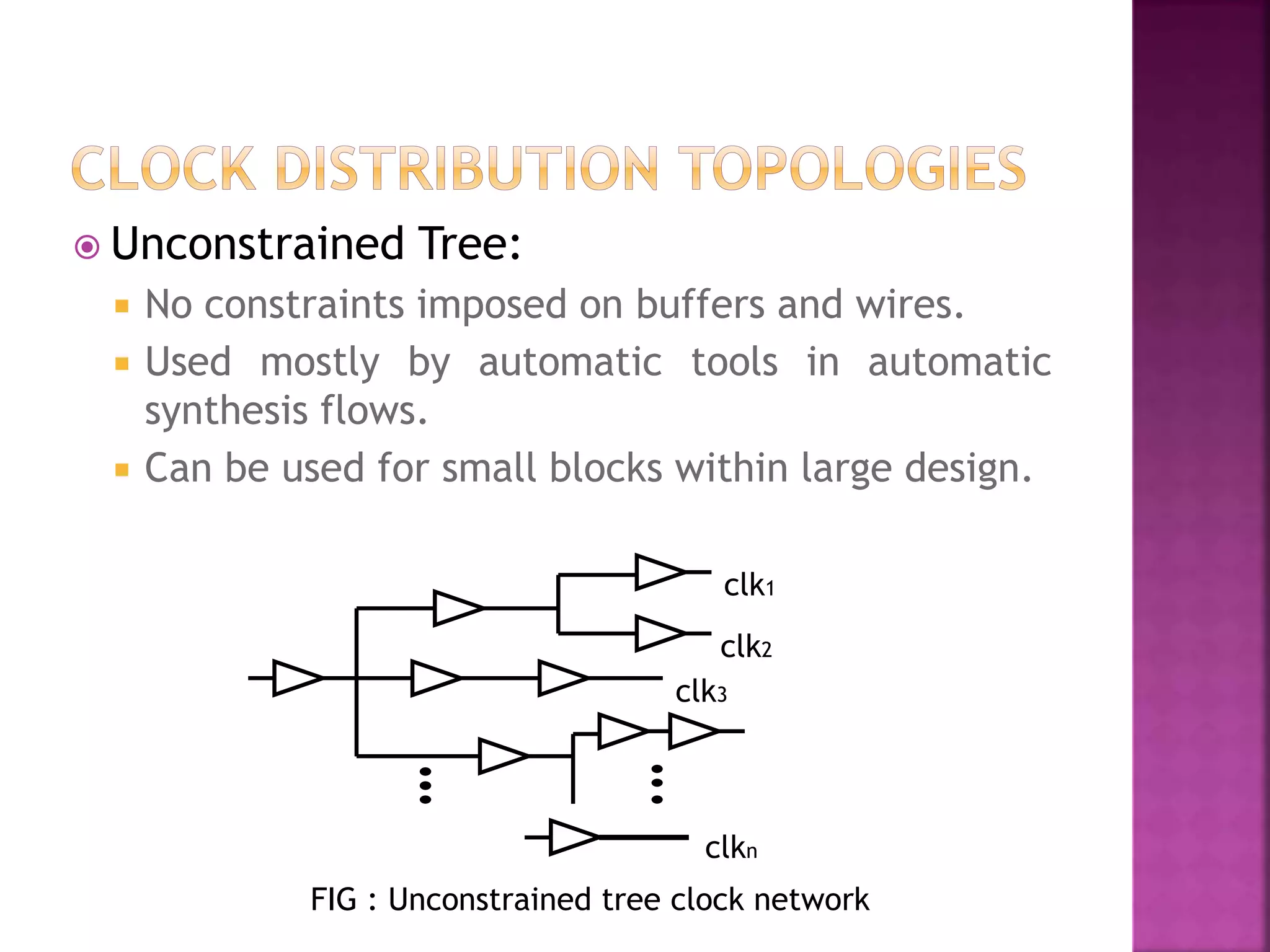
Unconstrained Tree:
No constraints imposed on buffers and wires.
Used mostly by automatic tools in automatic
synthesis flows.
Can be used for small blocks within large design.
clk1
clk2
clk3
clkn
FIG : Unconstrained tree clock network
8.
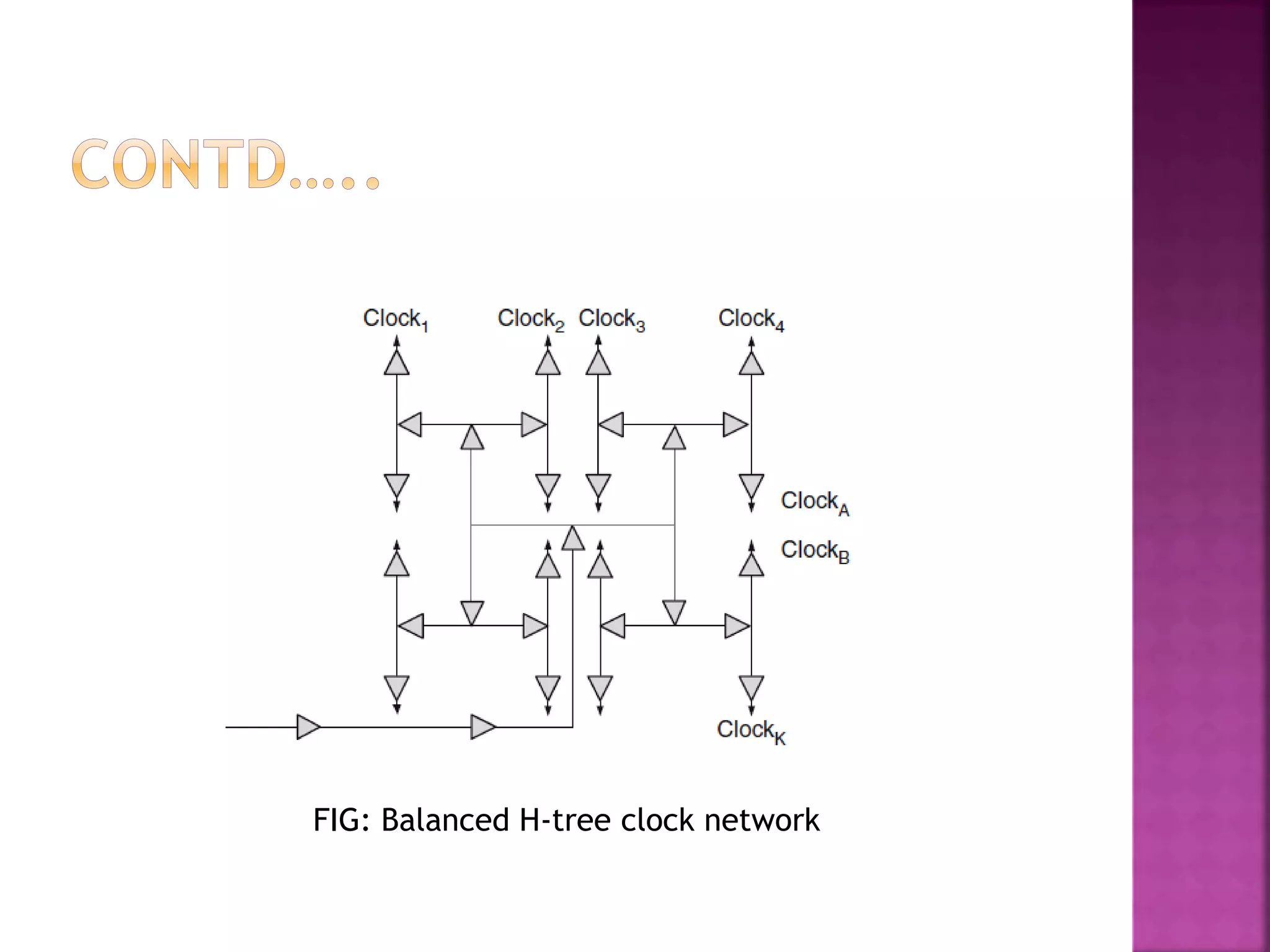
Balanced tree:
The length of interconnects is identical from the
source node n + 1 to the two destination nodes n.
The primary delay difference among the clock
signal paths is due to the variations of process
parameters affecting
Interconnect impedance
Characteristics of buffer
This structure is difficult to implement in
practice due to routing constraints and
different fan-out requirements.
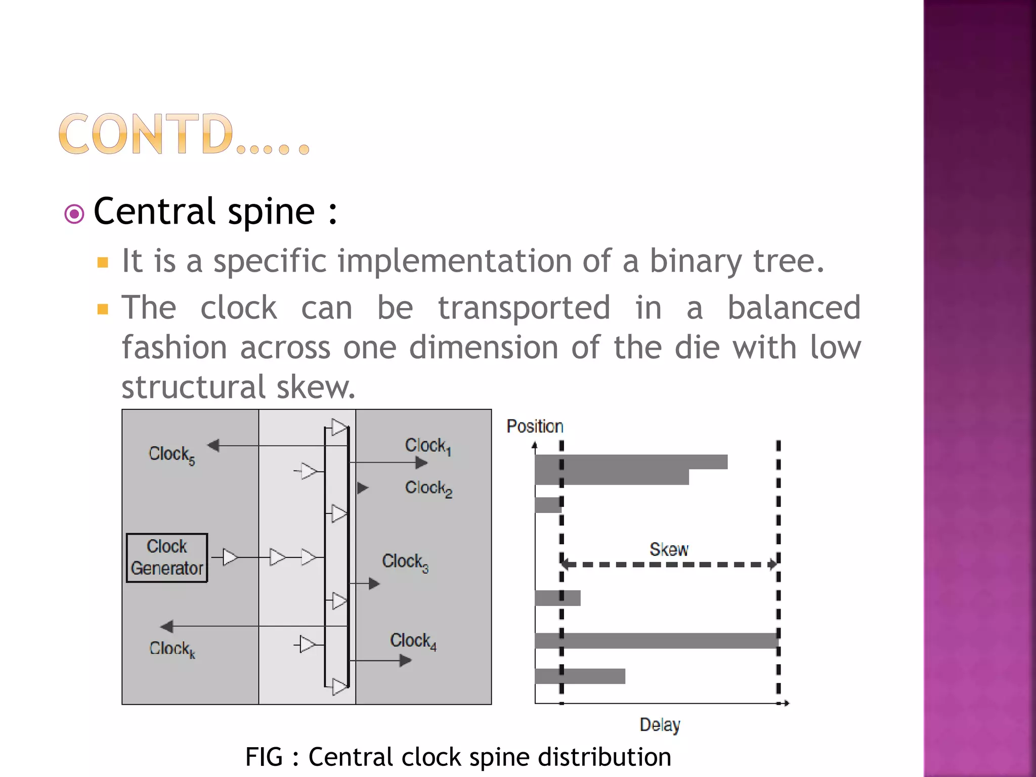
Central spine:
It is a specific implementation of a binary tree.
The clock can be transported in a balanced
fashion across one dimension of the die with low
structural skew.
FIG : Central clock spine distribution
11.
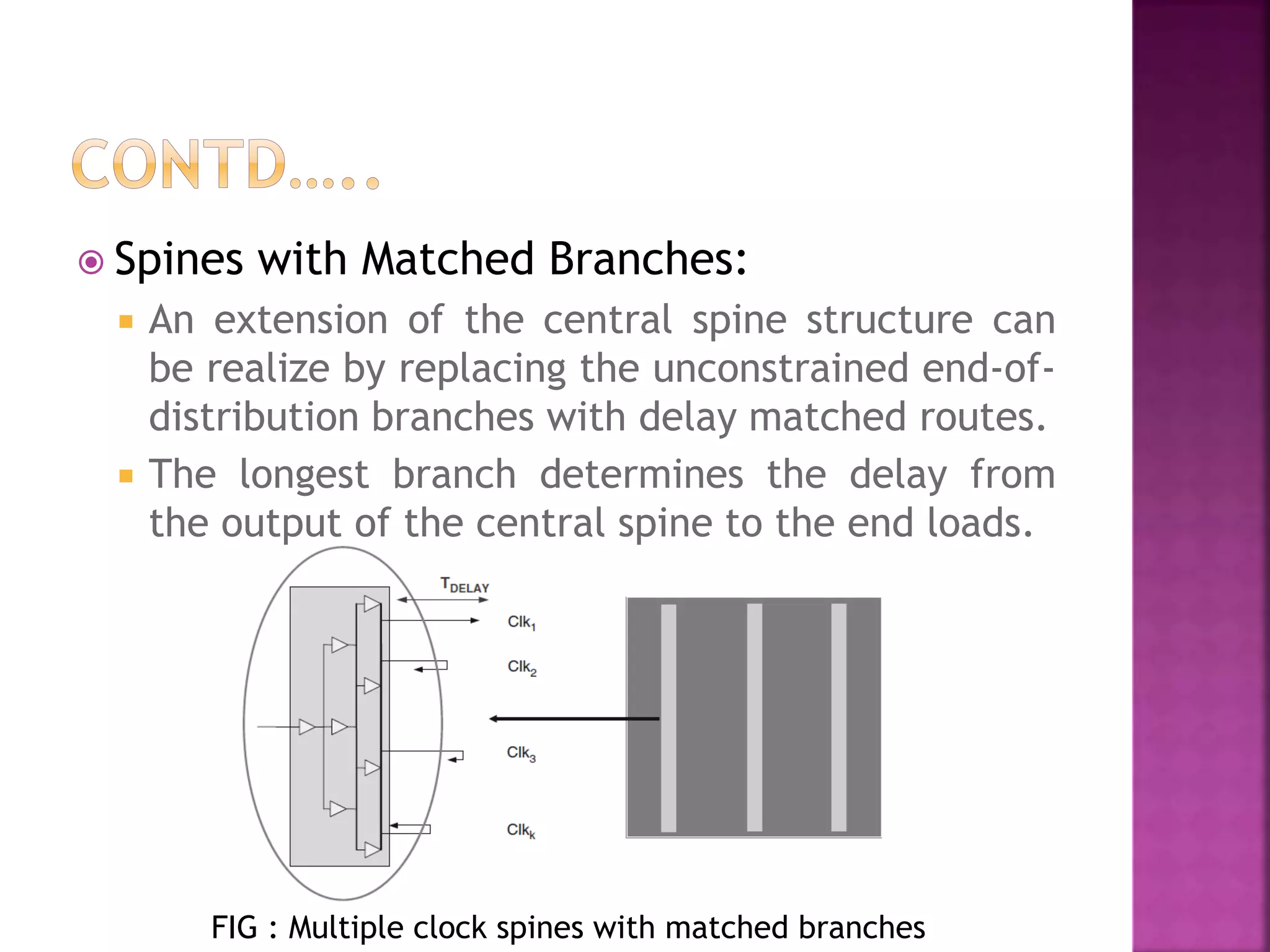
Spines withMatched Branches:
An extension of the central spine structure can
be realize by replacing the unconstrained end-of-distribution
branches with delay matched routes.
The longest branch determines the delay from
the output of the central spine to the end loads.
FIG : Multiple clock spines with matched branches
12.
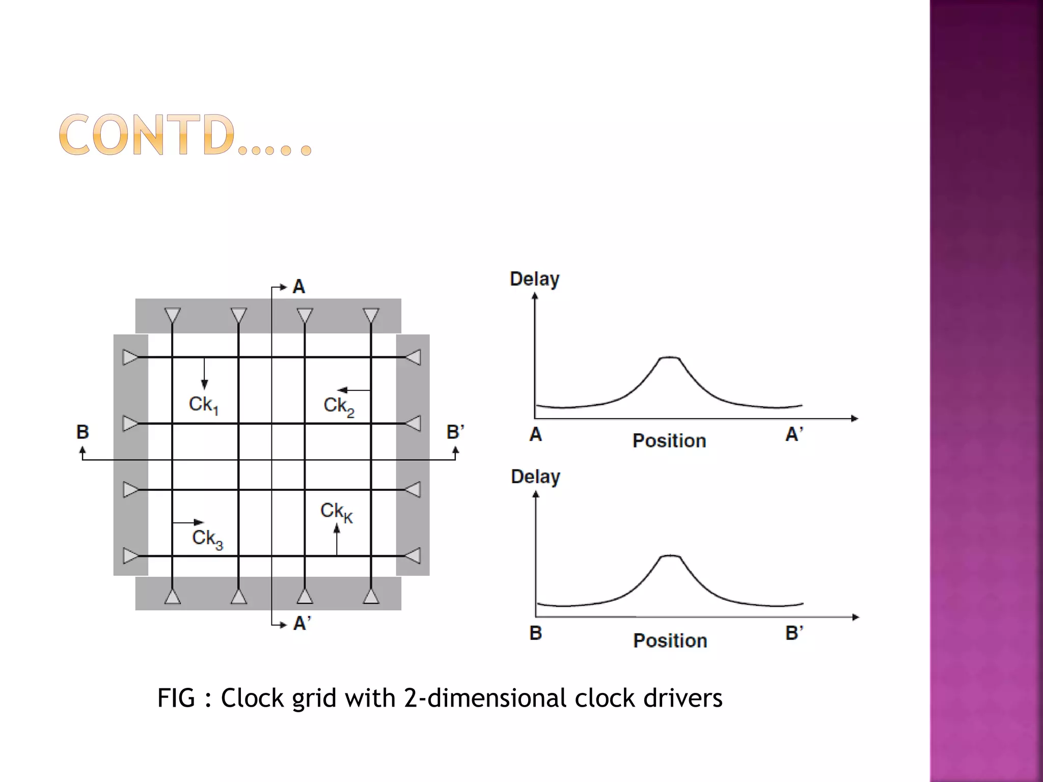
Grid :
This clock grid resembles a mesh with fully
connected clock tracks in both dimensions and
grid drivers located on all four sides.
Usually a custom implementation, simple to
build.
Insensitive to load changes.
Dissipate more power.
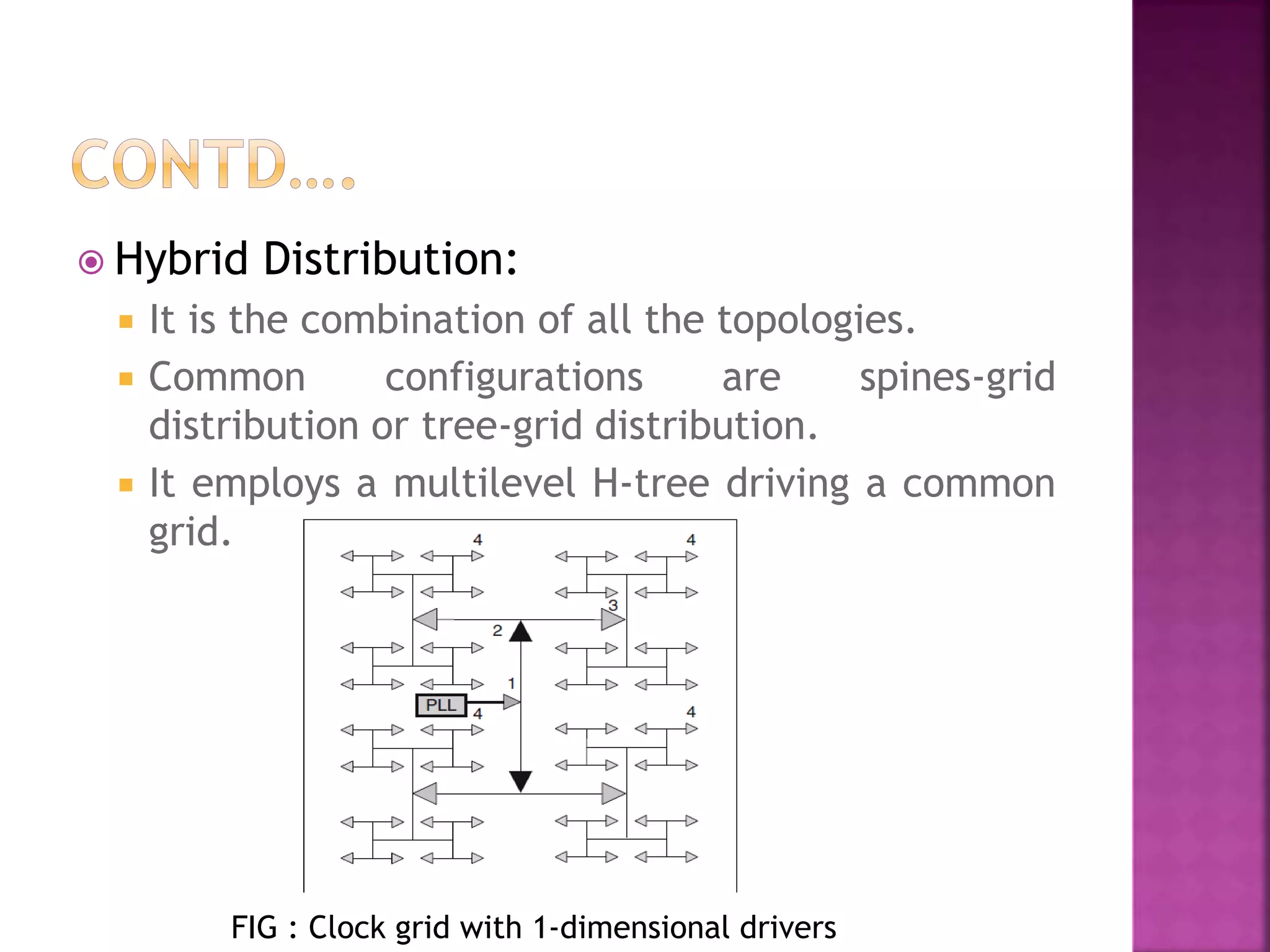
Hybrid Distribution:
It is the combination of all the topologies.
Common configurations are spines-grid
distribution or tree-grid distribution.
It employs a multilevel H-tree driving a common
grid.
FIG : Clock grid with 1-dimensional drivers