Download as PDF, PPTX


![3
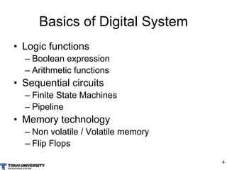
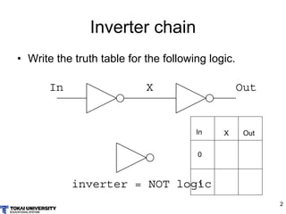
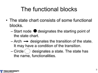
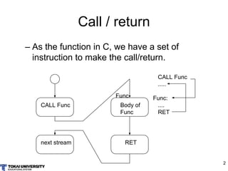
Bus Notations
• Use simple figure for multiple devices
– Ex: 4bit bus for Flip Flops, wires, multiplexors
thick line shows the bus
FF
QD
4
4InA
Out
InB
Sel
ck
0
1
4
4
FF
QD
Out[0]
FF
QD
Out[1]
FF
QD
Out[2]
FF
QD
Out[3]
InA[0]
InB[0]
Sel
0
1
InA[1]
InB[1]
Sel
0
1
InA[2]
InB[2]
Sel
0
1
InA[3]
InB[3]
Sel
0
1
ck
ck
ck
ck](https://image.slidesharecdn.com/computerdesign-170522154203/85/Computer-design-and-architecture-with-simple-cpu-42-320.jpg)
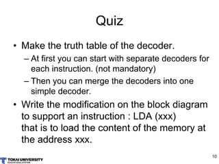
![11
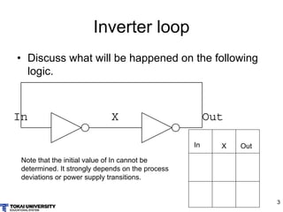
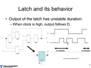
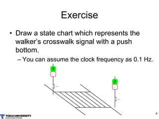
Quiz
• Complete the state chart
• Write the Boolean statement for “S > 1001 ||
o==1”
where S consists of S[0], S[1], S[2], S[3].
• Option [Draw the state machine of the BCD
adder controller.]](https://image.slidesharecdn.com/computerdesign-170522154203/85/Computer-design-and-architecture-with-simple-cpu-50-320.jpg)


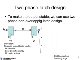
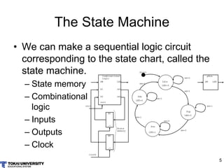
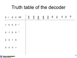
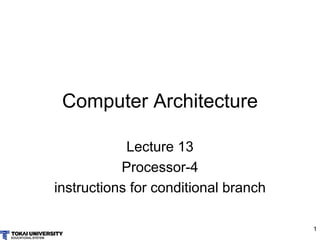
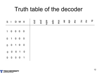
![11
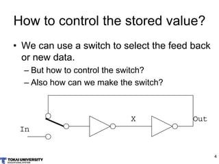
Quiz
• Make the truth table of the decoder.
– We only have an instruction LDA #xxx.
– The op binary format of LDA #xxx is 0x1002
– The input of the decoder is op[15:0], S,I,D,X
where op[15:12] designates the instruction,
op[3:0] designates the fn of ALU.
• Write the execution stage of an instruction
STA xxx
– The instrucition will write A into the memory.
– The op binary format of STA is 0x3000](https://image.slidesharecdn.com/computerdesign-170522154203/85/Computer-design-and-architecture-with-simple-cpu-61-320.jpg)
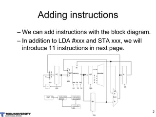


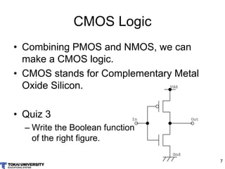
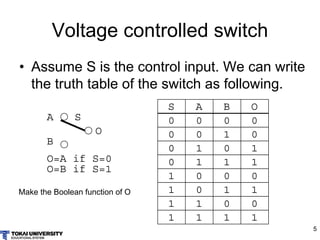
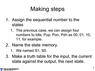
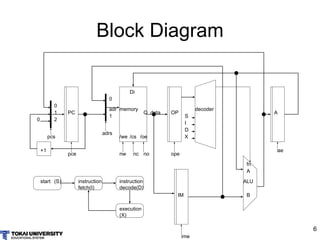
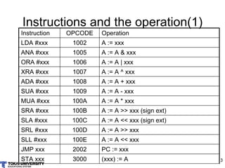
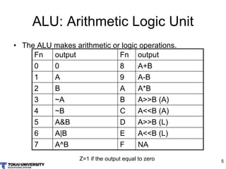
![2
Adding instructions
– We can add instructions utilizing memory data
with the block diagram. We modify the states.
PC OP
memoryadr
data
/cs /oe
+1
IM
Q
Di
/we
0
A
ope
ae
ime
pce
pcs
nw nonc
adrs
ALU
fn
A
B
0
0
1
1
2
decoder
start instruction
fetch(I)
instruction
decode(D)
execution
(X)
(S)
S
I
D
X
op
O
z
fe
F
F
memory
(M)
op[15]~op[15]](https://image.slidesharecdn.com/computerdesign-170522154203/85/Computer-design-and-architecture-with-simple-cpu-73-320.jpg)
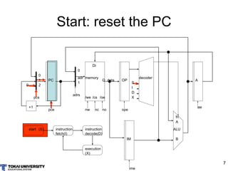
![6
Start: reset the PC
PC OP
memoryadr
data
/cs /oe
+1
IM
Q
Di
/we
0
A
ope
ae
ime
pce
pcs
nw nonc
adrs
ALU
fn
A
B
0
0
1
1
2
decoder
start instruction
fetch(I)
instruction
decode(D)
execution
(X)
(S)
S
I
D
X
op
O
z
fe
F
F
memory
(M)
op[15]~op[15]](https://image.slidesharecdn.com/computerdesign-170522154203/85/Computer-design-and-architecture-with-simple-cpu-77-320.jpg)
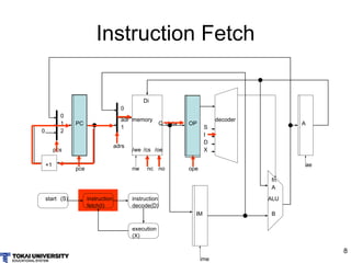
![7
Instruction Fetch (LDA 100)
PC OP
memoryadr
data
/cs /oe
+1
IM
Q
Di
/we
0
A
ope
ae
ime
pce
pcs
nw nonc
adrs
ALU
fn
A
B
0
0
1
1
2
decoder
start instruction
fetch(I)
instruction
decode(D)
execution
(X)
(S)
S
I
D
X
op
O
z
fe
F
F
memory
(M)
op[15]~op[15]](https://image.slidesharecdn.com/computerdesign-170522154203/85/Computer-design-and-architecture-with-simple-cpu-78-320.jpg)
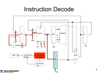
![8
Instruction Decode (LDA 100)
PC OP
memoryadr
data
/cs /oe
+1
IM
Q
Di
/we
0
A
ope
ae
ime
pce
pcs
nw nonc
adrs
ALU
fn
A
B
0
0
1
1
2
decoder
start instruction
fetch(I)
instruction
decode(D)
execution
(X)
(S)
S
I
D
X
op
O
z
fe
F
F
memory
(M)
op[15]~op[15]
100](https://image.slidesharecdn.com/computerdesign-170522154203/85/Computer-design-and-architecture-with-simple-cpu-79-320.jpg)
![9
PC OP
memoryadr
data
/cs /oe
+1
IM
Q
Di
/we
0
A
ope
ae
ime
pce
pcs
nw nonc
adrs
ALU
fn
A
B
0
0
1
1
2
decoder
start instruction
fetch(I)
instruction
decode(D)
execution
(X)
(S)
S
I
D
X
op
O
z
fe
F
F
memory
(M)
op[15]~op[15]
Memory (LDA 100)
100
(100)](https://image.slidesharecdn.com/computerdesign-170522154203/85/Computer-design-and-architecture-with-simple-cpu-80-320.jpg)
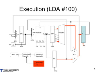
![10
Execution (LDA 100)
PC OP
memoryadr
data
/cs /oe
+1
IM
Q
Di
/we
0
A
ope
ae
ime
pce
pcs
nw nonc
adrs
ALU
fn
A
B
0
0
1
1
2
decoder
start instruction
fetch(I)
instruction
decode(D)
execution
(X)
(S)
S
I
D
X
op
O
z
fe
F
F
memory
(M)
op[15]~op[15]
(100)](https://image.slidesharecdn.com/computerdesign-170522154203/85/Computer-design-and-architecture-with-simple-cpu-81-320.jpg)

![6
Instruction Fetch (JZ 100)
PC OP
memoryadr
data
/cs /oe
+1
IM
Q
Di
/we
0
A
ope
ae
ime
pce
pcs
nw nonc
adrs
ALU
fn
A
B
0
0
1
1
2
decoder
start instruction
fetch(I)
instruction
decode(D)
execution
(X)
(S)
S
I
D
M
op
O
z Z
Z
memory
(M)
op[15]~op[15]
X](https://image.slidesharecdn.com/computerdesign-170522154203/85/Computer-design-and-architecture-with-simple-cpu-89-320.jpg)
![7
Instruction Decode (JZ 100)
100
PC OP
memoryadr
data
/cs /oe
+1
IM
Q
Di
/we
0
A
ope
ae
ime
pce
pcs
nw nonc
adrs
ALU
fn
A
B
0
0
1
1
2
decoder
start instruction
fetch(I)
instruction
decode(D)
execution
(X)
(S)
S
I
D
M
op
O
z Z
Z
memory
(M)
op[15]~op[15]
X](https://image.slidesharecdn.com/computerdesign-170522154203/85/Computer-design-and-architecture-with-simple-cpu-90-320.jpg)
![8
Execution (JZ 100 taken)
100
PC OP
memoryadr
data
/cs /oe
+1
IM
Q
Di
/we
0
A
ope
ae
ime
pce
pcs
nw nonc
adrs
ALU
fn
A
B
0
0
1
1
2
decoder
start instruction
fetch(I)
instruction
decode(D)
execution
(X)
(S)
S
I
D
M
op
O
z Z
Z
memory
(M)
op[15]~op[15]
X](https://image.slidesharecdn.com/computerdesign-170522154203/85/Computer-design-and-architecture-with-simple-cpu-91-320.jpg)
![9
PC OP
memoryadr
data
/cs /oe
+1
IM
Q
Di
/we
0
A
ope
ae
ime
pce
pcs
nw nonc
adrs
ALU
fn
A
B
0
0
1
1
2
decoder
start instruction
fetch(I)
instruction
decode(D)
execution
(X)
(S)
S
I
D
M
op
O
z Z
Z
memory
(M)
op[15]~op[15]
X
Execution (JZ 100 not taken)
100](https://image.slidesharecdn.com/computerdesign-170522154203/85/Computer-design-and-architecture-with-simple-cpu-92-320.jpg)

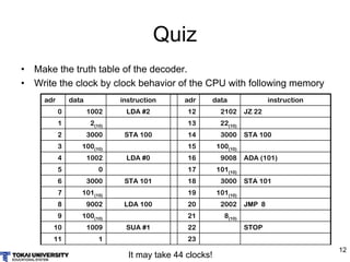
![11
Clock by clock behavior
clock instruction state PC OP IM A Z behavior
0 - S - - Set PC to 0
1 I 0 Instruction fetch from 0
Set OP to 1002
2 LDA #0 D 1 1002 Decode and fetch IM from 1
Set IM to 0
3 LDA #0 X 2 0 Set A to 0, Z to 1
4 I 2 0 1 Instruction fetch from 2
Set OP to 2102
5 JZ 0 D 3 2102 Decode and fetch IM from 3
Set IM to 0
6 JZ 0 X 4 0 On Z=1, jump to 0
7 I 0 Instruction fetch from 0
Set OP to 1002
8 LDA #0 D 1 Decode and fetch IM from 1
Set IM to 0
9 LDA #0 X 2 0 Set A to 0, Z to 1
adr data instruction
0 1002 LDA #0
1 0(10)
2 2102 JZ 0
3 0
Memory contents
PC OP
memoryadr
data
/cs /oe
+1
IM
Q
Di
/we
0
A
ope
ae
ime
pce
pcs
nw nonc
adrs
ALU
fn
A
B
0
0
1
1
2
decoder
start instruction
fetch(I)
instruction
decode(D)
execution
(X)
(S)
S
I
D
M
op
O
z Z
Z
memory
(M)
op[15]~op[15]
X](https://image.slidesharecdn.com/computerdesign-170522154203/85/Computer-design-and-architecture-with-simple-cpu-94-320.jpg)
![6
Instruction Fetch (CALL 100)
PC OP
memoryadr
data
/cs /oe
+1
IM
Q
Di
/we
0
A
ope
ae
ime
pce
pcs
nw nonc
adrs
ALU
fn
A
B
0
0
1
1
2
decoder
start instruction
fetch(I)
instruction
decode(D)
execution
(X)
(S)
S
I
D
M
op
O
z Z
Z
memory
(M)
op[15]~op[15]
X
ST
ste
3](https://image.slidesharecdn.com/computerdesign-170522154203/85/Computer-design-and-architecture-with-simple-cpu-101-320.jpg)
![7
Instruction Decode (CALL 100)
100
PC OP
memoryadr
data
/cs /oe
+1
IM
Q
Di
/we
0
A
ope
ae
ime
pce
pcs
nw nonc
adrs
ALU
fn
A
B
0
0
1
1
2
decoder
start instruction
fetch(I)
instruction
decode(D)
execution
(X)
(S)
S
I
D
M
op
O
z Z
Z
memory
(M)
op[15]~op[15]
X
ST
ste
3](https://image.slidesharecdn.com/computerdesign-170522154203/85/Computer-design-and-architecture-with-simple-cpu-102-320.jpg)
![8
Execution (CALL 100)
100
PC OP
memoryadr
data
/cs /oe
+1
IM
Q
Di
/we
0
A
ope
ae
ime
pce
pcs
nw nonc
adrs
ALU
fn
A
B
0
0
1
1
2
decoder
start instruction
fetch(I)
instruction
decode(D)
execution
(X)
(S)
S
I
D
M
op
O
z Z
Z
memory
(M)
op[15]~op[15]
X
ST
ste
3](https://image.slidesharecdn.com/computerdesign-170522154203/85/Computer-design-and-architecture-with-simple-cpu-103-320.jpg)
![9
Instruction Fetch (RET)
PC OP
memoryadr
data
/cs /oe
+1
IM
Q
Di
/we
0
A
ope
ae
ime
pce
pcs
nw nonc
adrs
ALU
fn
A
B
0
0
1
1
2
decoder
start instruction
fetch(I)
instruction
decode(D)
execution
(X)
(S)
S
I
D
M
op
O
z Z
Z
memory
(M)
op[15]~op[15]
X
ST
ste
3](https://image.slidesharecdn.com/computerdesign-170522154203/85/Computer-design-and-architecture-with-simple-cpu-104-320.jpg)
![10
Instruction Decode (RET)
PC OP
memoryadr
data
/cs /oe
+1
IM
Q
Di
/we
0
A
ope
ae
ime
pce
pcs
nw nonc
adrs
ALU
fn
A
B
0
0
1
1
2
decoder
start instruction
fetch(I)
instruction
decode(D)
execution
(X)
(S)
S
I
D
M
op
O
z Z
Z
memory
(M)
op[15]~op[15]
X
ST
ste
3](https://image.slidesharecdn.com/computerdesign-170522154203/85/Computer-design-and-architecture-with-simple-cpu-105-320.jpg)
![11
Execution (RET)
PC OP
memoryadr
data
/cs /oe
+1
IM
Q
Di
/we
0
A
ope
ae
ime
pce
pcs
nw nonc
adrs
ALU
fn
A
B
0
0
1
1
2
decoder
start instruction
fetch(I)
instruction
decode(D)
execution
(X)
(S)
S
I
D
M
op
O
z Z
Z
memory
(M)
op[15]~op[15]
X
ST
ste
3](https://image.slidesharecdn.com/computerdesign-170522154203/85/Computer-design-and-architecture-with-simple-cpu-106-320.jpg)
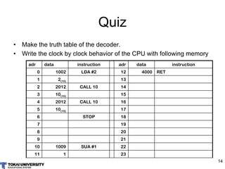
![13
Clock by clock behavior
adr data instruction
0 2012 CALL
1 10 10
2 ---- STOP
10 4000 RET
Memory contents
PC OP
memoryadr
data
/cs /oe
+1
IM
Q
Di
/we
0
A
ope
ae
ime
pce
pcs
nw nonc
adrs
ALU
fn
A
B
0
0
1
1
2
decoder
start instruction
fetch(I)
instruction
decode(D)
execution
(X)
(S)
S
I
D
M
op
O
z Z
Z
memory
(M)
op[15]~op[15]
X
ST
ste
3
clock instruction state PC OP IM A ST behavior
0 - S - - Set PC to 0
1 I 0 Instruction fetch from 0
Set OP to 2012
2 CALL D 1 2012 Decode and fetch IM
from 1
Set IM to 10
3 X 2 10 Set PC to 10, ST to PC
4 I 10 2 Instruction fetch from 10,
Set OP to 4000
5 RET D 11 4000 Decode
6 X Set PC to value of ST
7 I 2 STOP](https://image.slidesharecdn.com/computerdesign-170522154203/85/Computer-design-and-architecture-with-simple-cpu-108-320.jpg)

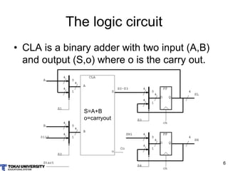
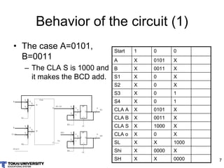
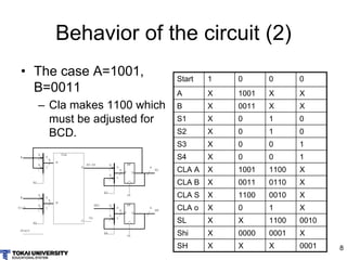
This document describes the design of a binary coded decimal (BCD) adder circuit using a binary adder and additional logic. It explains that BCD represents numbers from 0-9 using 4-bit codes and involves adding 6 to results exceeding 9. The circuit uses a carry lookahead adder (CLA) to compute the sum and carry out of the binary addition. Additional logic checks if the sum exceeds 9, and if so adds 6 to the sum and sets the carry flag. The circuit correctly performs BCD addition and adjusts results to valid BCD codes. Behavior examples are provided for sample additions.