1
1
Today: Sequential Circuits
(H&H 3.1-3.6, 5.4)
Next: continued
Lecture Topics
2
Self-study module #2 (this week)
Project #1 scores sent via email yesterday
Project #2 (due no later than 9/12)
Project #3 (due no later than 9/19)
Announcements
2
3
• Combinational circuits have no "memory":
the output is determined by the current
inputs.
• Sequential circuits "remember" the current
state: the output is determined by the
current inputs and the current state.
Sequential Circuits
4
• A vending machine must remember how many
coins and what kinds of coins have been inserted.
The behavior is based not only on the current coin
inserted (current input), but also on how many and
what kinds of coins have been inserted previously
(current state).
• These are referred to as finite state machines
(finite state automata).
Example: vending machine
3
5
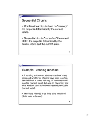
Example FSM
Transition Table
0 1
00 01 10
01 11 01
10 10 11
11 11 11
00
01
10
11
0
1
0
0,1
1
0
1
6
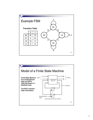
Model of a Finite State Machine
Finite State Machine
has combinational
logic and DFFs
(data flip-flops) in a
feedback loop.
The DFFs maintain
state information.
4
7
D Flip-flop
Positive edge-triggered D flip-flop: the value of D is copied into
the flip-flop (and becomes the value of Q) when C changes
from 0 to 1.
8
Clock Waveform
• Clock pulse "edges"
Rising edge (leading edge, positive edge)
Falling edge (trailing edge, negative edge)
• A clock cycle of 25 ns equals a clock rate of 40 MHz
5
9
S-R Latch
• The S input sets the latch (forces it to contain a 1)
• The R input resets the latch (forces it to contain a 0)
10
NAND and NOR Gates
6
11
Four cases:
• S = 1, R = 0
• S = 0, R = 1
• S = 0, R = 0
• S = 1, R =1
Analysis: SR Latch
R
S
Q
Q
N1
N2
12
Analysis: SR Latch
if S = 1, R = 0 then
Q = 1, Q' = 0
(Set the latch)
if S = 0, R = 1 then
Q = 0, Q' = 1
(Reset the latch)
R
S
Q
Q
N1
N2
1
0
0
1
0
1
R
S
Q
Q
N1
N2
0
1
1
0
0
0
1
7
13
Analysis: SR Latch
if S = 0, R = 0 then
no change to Q, Q'
(Keep previous Q)
R
S
Q
Q
N1
N2
0
0
R
S
Q
Q
N1
N2
0
0
0
Qprev
= 0 Qprev
= 1
1
14
Analysis: SR Latch
if S = 1, R = 1 then
Q = 0, Q' = 0
(Invalid!)
Cannot set and
reset the latch
simultaneously
Note: Q ≠ NOT Q'
R
S
Q
Q
N1
N2
1
1
0
0
0
0
8
15
Using NOR gates
(active high)
Using NAND gates
(active low)
S-R Latch
16
Gated S-R Latch
The Enable signal
(usually a clock signal)
controls the NAND gates
(which control the S and
R inputs)
9
17
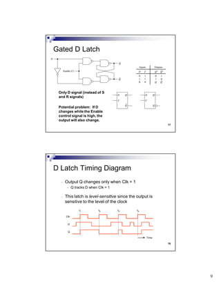
Gated D Latch
Only D signal (instead of S
and R signals)
Potential problem: If D
changes while the Enable
control signal is high, the
output will also change.
18
o Output Q changes only when Clk = 1
• Q tracks D when Clk = 1
o This latch is level-sensitive since the output is
sensitive to the level of the clock
D Latch Timing Diagram
t1 t2 t3 t4
Time
Clk
D
Q
10
19
Master-Slave D Flip-Flop
Want changes in Q only on the transition of the Clk signal
from 1 0 (or from 0 1)
When Clock = 1, master latch tracks D; slave latch remains
unchanged (Q remains fixed)
When Clock = 0, master latch is unchanged; slave latch tracks Qm
D Q
Q
Master Slave
D
Clock
Q
Q
D Q
Q
Q
ClkClk
D Q
Q
negative edge-triggered flip-flop
20
Timing of Master-Slave D Flip-Flop
Changes to Q occur only on the negative edge of the Clock
D Q
Q
Master Slave
D
Clock
Q
Q
D Q
Q
Q m Q s
ClkClk
D
Clock
Q m
Q Q s=
11
21
Negative Edge-Triggered DFF
• When CLK is high, the
two input latches contain
0, so the Main latch
remains in its previous
state, regardless of any
changes to D.
• On the falling edge of
CLK, values in the two
input latches will affect the
state of the Main latch.
• While CLK is low, D
cannot affect the Main
latch.
22
Positive Edge-Triggered DFF
D
Clock
P4
P3
P1
P2
5
6
1
2
3
Q
Q
4
12
23
Asynchronous Clear and Preset (active low)
DFF with Clear and Preset
D
Clock
Q
Q
Clear
Preset
Preset
Clear
D Q
Q
24
Commercial D Flip-flop
Q
Q
PRE
D
CLR
CLK
PRE
CLR
Q
Q
Q
Q
Asynchronous controls
(active low):
PRE' – force to 1 (preset)
CLR' – force to 0 (clear)
D
CLK
13
25
Commercial D Flip-flop
PRE' CLR' D CLK Q Q' Mode
0 0 X X 1 1 Not allowed
0 1 X X 1 0 Set
1 0 X X 0 1 Clear
1 1 X 0 Qn-1 Q'n-1 Hold
1 1 X 1 Qn-1 Q'n-1 Hold
1 1 0 0 1 Clocked operation
1 1 1 1 0 Clocked operation
26
State info in FSM
o Counter
o Sequencer
Data storage
o Register with parallel load
o Register file (collection of registers)
Uses of Data Flip-flops
14
27
Standard Up Counter
o Sequence starts at 0, counts up by 1
o Starts over after reaching max
Example: 2-bit Up Counter
0, 1, 2, 3, 0, 1, 2, 3, 0, …
Variations: count down, count by 2, etc.
Counters
28
Output: 000, 001, 010, 011, 100, 101, 110, 111, 000, …
3-bit Up Counter
3
Reset
Clock
Output
15
29
Output: 000, 001, 010, 011, 100, 101, 110, 111, 000, …
Three DFFs used to store current state
Combinational logic used to determine next state
Reset: initialize DFFs to state 000
Clock: copy next state into DFFs
3-bit Up Counter
30
Design of 3-bit Up Counter
Three separate
functions:
N2(C2, C1, C0) = ….
N1(C2, C1, C0) = ….
N0(C2, C1, C0) = ….
C2 C1 C0 N2 N1 N0
0 0 0 0 0 1
0 0 1 0 1 0
0 1 0 0 1 1
0 1 1 1 0 0
1 0 0 1 0 1
1 0 1 1 1 0
1 1 0 1 1 1
1 1 1 0 0 0
16
31
N2(C2, C1, C0) = C2C1' + C2C0' + C2'C1C0
Karnaugh Map for N2
C2C1
00 01 11 10
C0
0 0 0 1 1
1 0 1 0 1
32
N1(C2, C1, C0) = C1'C0 + C1C0'
Karnaugh Map for N1
C2C1
00 01 11 10
C0
0 0 1 1 0
1 1 0 0 1
17
33
N0(C2, C1, C0) = C0'
Karnaugh Map for N0
C2C1
00 01 11 10
C0
0 1 1 1 1
1 0 0 0 0
34
Generate signals for N steps in a cycle
o N bits of output
o Exactly 1 bit asserted at each step
Example: 5-bit Sequencer
10000, 01000, 00100, 00010, 00001, 10000, …
Sequencers
18
35
3-bit Sequencer
Output: 100, 010, 001, 100, 010, 001, 100, …
3
ResetClock
Output
36
3-bit Sequencer
Output: 100, 010, 001, 100, 010, 001, 100, …
Q
QB
SET
CLEAR
D Q
QB
SET
CLEAR
D Q
QB
SET
CLEAR
D
Reset
O2 O1 O0
1
1
Today: Sequential Circuits
(H&H 3.1-3.6, 5.4)
Next: Integer Arithmetic
(H&H 5.1-5.2)
Lecture Topics
2
Self-study module #3
Project #3 (due no later than 9/19)
Project #4 (due no later than 9/26)
Announcements
2
3
Due Thursday, 9/19 (by 11:59 PM)
Focuses on implementation of circuits you
designed for Project #2
o review handout
o review notes file
o complete Self-study Exercise #2
Computer Project #3
4
• Combinational circuits have no "memory":
the output is determined by the current
inputs.
• Sequential circuits "remember" the current
state: the output is determined by the
current inputs and the current state.
Sequential Circuits
3
5
Model of a Finite State Machine
Finite State Machine
has combinational
logic and DFFs
(data flip-flops) in a
feedback loop.
The DFFs maintain
state information.
6
Commercial D Flip-flop
Q
Q
PRE
D
CLR
CLK
PRE
CLR
Q
Q
Q
Q
Asynchronous controls
(active low):
PRE' – force to 1 (preset)
CLR' – force to 0 (clear)
D
CLK
4
7
Commercial D Flip-flop
PRE' CLR' D CLK Q Q' Mode
0 0 X X 1 1 Not allowed
0 1 X X 1 0 Set
1 0 X X 0 1 Clear
1 1 X 0 Qn-1 Q'n-1 Hold
1 1 X 1 Qn-1 Q'n-1 Hold
1 1 0 0 1 Clocked operation
1 1 1 1 0 Clocked operation
8
State info in FSM
o Counter
o Sequencer
Data storage
o Register with parallel load
o Register file (collection of registers)
Uses of Data Flip-flops
5
9
Standard Up Counter
o Sequence starts at 0, counts up by 1
o Starts over after reaching max
Example: 2-bit Up Counter
0, 1, 2, 3, 0, 1, 2, 3, 0, …
Variations: count down, count by 2, etc.
Counters
10
Output: 000, 001, 010, 011, 100, 101, 110, 111, 000, …
3-bit Up Counter
3
Reset
Clock
Output
6
11
Output: 000, 001, 010, 011, 100, 101, 110, 111, 000, …
Three DFFs used to store current state
Combinational logic used to determine next state
Reset: initialize DFFs to state 000
Clock: copy next state into DFFs
3-bit Up Counter
12
Design of 3-bit Up Counter
Three separate
functions:
N2(C2, C1, C0) = ….
N1(C2, C1, C0) = ….
N0(C2, C1, C0) = ….
C2 C1 C0 N2 N1 N0
0 0 0 0 0 1
0 0 1 0 1 0
0 1 0 0 1 1
0 1 1 1 0 0
1 0 0 1 0 1
1 0 1 1 1 0
1 1 0 1 1 1
1 1 1 0 0 0
7
13
N2(C2, C1, C0) = C2C1' + C2C0' + C2'C1C0
Karnaugh Map for N2
C2C1
00 01 11 10
C0
0 0 0 1 1
1 0 1 0 1
14
N1(C2, C1, C0) = C1'C0 + C1C0'
Karnaugh Map for N1
C2C1
00 01 11 10
C0
0 0 1 1 0
1 1 0 0 1
8
15
N0(C2, C1, C0) = C0'
Karnaugh Map for N0
C2C1
00 01 11 10
C0
0 1 1 1 1
1 0 0 0 0
16
Generate signals for N steps in a cycle
o N bits of output
o Exactly 1 bit asserted at each step
Example: 5-bit Sequencer
10000, 01000, 00100, 00010, 00001, 10000, …
Sequencers
9
17
3-bit Sequencer
Output: 100, 010, 001, 100, 010, 001, 100, …
3
ResetClock
Output
18
3-bit Sequencer
Output: 100, 010, 001, 100, 010, 001, 100, …
Q
QB
SET
CLEAR
D Q
QB
SET
CLEAR
D Q
QB
SET
CLEAR
D
Reset
O2 O1 O0
10
19
N-bit register with parallel load
o N bits of input
o N bits of output
o Input copied into register in parallel
(simultaneously, on clock pulse)
o Input becomes output
o Value retained until deliberately replaced
Registers
20
4-bit Register using DFFs
Q 3 Q 2 Q 1 Q 0
Clock
Parallel input
Parallel output
D Q
Q
D Q
Q
D Q
Q
D Q
Q
11
21
4-bit Register with Load Control
Q 3 Q 2 Q 1 Q 0
Clock
Parallel input
Parallel output
D Q
Q
D Q
Q
D Q
Q
D Q
Q
Load
22
Copying a value into a register
Assume 8-bit register:
Place 8-bit value on D
Assert Load
Wait for Clock pulse
De-assert Load
D0-7 Q0-7D0-7
Q0-7
Clock
8 8
Load
12
23
Register File and ALU
Register
File ALU
24
Register File
N registers
2 output ports
1 input port
Read register 1 selects
register for Read data 1
Read register 2 selects
register for Read data 2
Write register selects
register for Write data
13
25
Register File
Select the two
source registers
using two banks
of multiplexers
26
Register File
Select destination
register using a
decoder
14
27
Multi-bit MUX
High-level view:
32-bit 2-to-1 MUX
Implementation:
32 individual 2-to-1
MUXes controled by
same Select signal
28
We need to distinguish between three things
when talking about a data item:
Value
External representation
Internal representation
Data Representation
15
29
External representations:
12 base 10
C base 16
1100 base 2
(many others)
Internal representation (in 8 bits):
00001100
Example: the value twelve
30
Computing systems can directly process:
Boolean data
Character data
Unsigned integer data
Signed integer data
Floating point data
First four processed in integer circuits, last
one processed in floating point circuits
Fundamental Data Types
16
31
Only two values: false, true
Normally stored in 8-bit byte or 32-bit word:
false: 0
true: any other bit pattern
Processed as unsigned integers in circuits
Boolean Data
32
Internal representation uses a fixed number
of bits to represent each character in the set
ASCII (7 bits)
~cse320/Examples/example01.pdf
Unicode (8, 16 or 32 bits)
Character Data
17
33
Character set includes characters from
typewriter keyboard:
52 letters (Latin alphabet, 26 upper and lower)
10 digits
33 symbols
33 control codes
Stored one character per 8-bit byte
ASCII
34
Upper case letters:
A 1000001
B 1000010
C 1000011
…
Y 1011001
Z 1011010
Examples
18
35
Code numbers (bit patterns) used for
comparisons and sorting
Characters within sequences are in order:
Upper case letters
Lower case letters
Decimal digits
Other characters not in any logical order
Notes about ASCII
36
Processed as unsigned integers in circuits
Examples:
'A' + 1 ==> 'B'
'B' - 'A' ==> 1
'A' < 'B' ==> true
Notes about ASCII
19
37
Internal representation uses a fixed number
of bits to represent each character in the set
ASCII table
~cse320/Examples/example01.pdf
Internal representation
~cse320/Examples/example02.pdf
Summary: Character Data
38
Expressed in base 2, with leading zeroes
Set of values starts at zero, limited by
number of bits available for storage
Example: 8-bit bytes
min: 00000000 0
max: 11111111 255 (28 – 1)
Unsigned Integers
20
39
Assume 16 bits:
0 0000000000000000
1 0000000000000001
2 0000000000000010
3 0000000000000011
4 0000000000000100
Examples
40
Expressed in base 2, with leading zeroes
Set of values starts at zero, limited by
number of bits available for storage
Internal representation
~cse320/Examples/example03.pdf
Summary: Unsigned Integers
21
41
Negative representation formed by applying
two’s complement operation to all bits in
positive representation (flip all bits, add 1)
Example (assume 8 bits):
+25 00011001
-25 11100111
Two’s Complement
42
Range (assume 8 bits):
max 01111111 +(27 – 1)
min 10000000 -(27)
One representation of zero (assume 8 bits):
+0 00000000
-0 00000000
Two’s Complement
22
43
Internal representation (8 bits):
+21: 00010101
flip bits: 11101010
add 1: 1
--------
-21: 11101011
Example: -21 base 10
44
Internal representation (8 bits):
+22: 00010110
flip bits: 11101001
add 1: 1
--------
-22: 11101010
Example: -22 base 10

Chapter 3

  • 1.
    1 1 Today: Sequential Circuits (H&H3.1-3.6, 5.4) Next: continued Lecture Topics 2 Self-study module #2 (this week) Project #1 scores sent via email yesterday Project #2 (due no later than 9/12) Project #3 (due no later than 9/19) Announcements
  • 2.
    2 3 • Combinational circuitshave no "memory": the output is determined by the current inputs. • Sequential circuits "remember" the current state: the output is determined by the current inputs and the current state. Sequential Circuits 4 • A vending machine must remember how many coins and what kinds of coins have been inserted. The behavior is based not only on the current coin inserted (current input), but also on how many and what kinds of coins have been inserted previously (current state). • These are referred to as finite state machines (finite state automata). Example: vending machine
  • 3.
    3 5 Example FSM Transition Table 01 00 01 10 01 11 01 10 10 11 11 11 11 00 01 10 11 0 1 0 0,1 1 0 1 6 Model of a Finite State Machine Finite State Machine has combinational logic and DFFs (data flip-flops) in a feedback loop. The DFFs maintain state information.
  • 4.
    4 7 D Flip-flop Positive edge-triggeredD flip-flop: the value of D is copied into the flip-flop (and becomes the value of Q) when C changes from 0 to 1. 8 Clock Waveform • Clock pulse "edges" Rising edge (leading edge, positive edge) Falling edge (trailing edge, negative edge) • A clock cycle of 25 ns equals a clock rate of 40 MHz
  • 5.
    5 9 S-R Latch • TheS input sets the latch (forces it to contain a 1) • The R input resets the latch (forces it to contain a 0) 10 NAND and NOR Gates
  • 6.
    6 11 Four cases: • S= 1, R = 0 • S = 0, R = 1 • S = 0, R = 0 • S = 1, R =1 Analysis: SR Latch R S Q Q N1 N2 12 Analysis: SR Latch if S = 1, R = 0 then Q = 1, Q' = 0 (Set the latch) if S = 0, R = 1 then Q = 0, Q' = 1 (Reset the latch) R S Q Q N1 N2 1 0 0 1 0 1 R S Q Q N1 N2 0 1 1 0 0 0 1
  • 7.
    7 13 Analysis: SR Latch ifS = 0, R = 0 then no change to Q, Q' (Keep previous Q) R S Q Q N1 N2 0 0 R S Q Q N1 N2 0 0 0 Qprev = 0 Qprev = 1 1 14 Analysis: SR Latch if S = 1, R = 1 then Q = 0, Q' = 0 (Invalid!) Cannot set and reset the latch simultaneously Note: Q ≠ NOT Q' R S Q Q N1 N2 1 1 0 0 0 0
  • 8.
    8 15 Using NOR gates (activehigh) Using NAND gates (active low) S-R Latch 16 Gated S-R Latch The Enable signal (usually a clock signal) controls the NAND gates (which control the S and R inputs)
  • 9.
    9 17 Gated D Latch OnlyD signal (instead of S and R signals) Potential problem: If D changes while the Enable control signal is high, the output will also change. 18 o Output Q changes only when Clk = 1 • Q tracks D when Clk = 1 o This latch is level-sensitive since the output is sensitive to the level of the clock D Latch Timing Diagram t1 t2 t3 t4 Time Clk D Q
  • 10.
    10 19 Master-Slave D Flip-Flop Wantchanges in Q only on the transition of the Clk signal from 1 0 (or from 0 1) When Clock = 1, master latch tracks D; slave latch remains unchanged (Q remains fixed) When Clock = 0, master latch is unchanged; slave latch tracks Qm D Q Q Master Slave D Clock Q Q D Q Q Q ClkClk D Q Q negative edge-triggered flip-flop 20 Timing of Master-Slave D Flip-Flop Changes to Q occur only on the negative edge of the Clock D Q Q Master Slave D Clock Q Q D Q Q Q m Q s ClkClk D Clock Q m Q Q s=
  • 11.
    11 21 Negative Edge-Triggered DFF •When CLK is high, the two input latches contain 0, so the Main latch remains in its previous state, regardless of any changes to D. • On the falling edge of CLK, values in the two input latches will affect the state of the Main latch. • While CLK is low, D cannot affect the Main latch. 22 Positive Edge-Triggered DFF D Clock P4 P3 P1 P2 5 6 1 2 3 Q Q 4
  • 12.
    12 23 Asynchronous Clear andPreset (active low) DFF with Clear and Preset D Clock Q Q Clear Preset Preset Clear D Q Q 24 Commercial D Flip-flop Q Q PRE D CLR CLK PRE CLR Q Q Q Q Asynchronous controls (active low): PRE' – force to 1 (preset) CLR' – force to 0 (clear) D CLK
  • 13.
    13 25 Commercial D Flip-flop PRE'CLR' D CLK Q Q' Mode 0 0 X X 1 1 Not allowed 0 1 X X 1 0 Set 1 0 X X 0 1 Clear 1 1 X 0 Qn-1 Q'n-1 Hold 1 1 X 1 Qn-1 Q'n-1 Hold 1 1 0 0 1 Clocked operation 1 1 1 1 0 Clocked operation 26 State info in FSM o Counter o Sequencer Data storage o Register with parallel load o Register file (collection of registers) Uses of Data Flip-flops
  • 14.
    14 27 Standard Up Counter oSequence starts at 0, counts up by 1 o Starts over after reaching max Example: 2-bit Up Counter 0, 1, 2, 3, 0, 1, 2, 3, 0, … Variations: count down, count by 2, etc. Counters 28 Output: 000, 001, 010, 011, 100, 101, 110, 111, 000, … 3-bit Up Counter 3 Reset Clock Output
  • 15.
    15 29 Output: 000, 001,010, 011, 100, 101, 110, 111, 000, … Three DFFs used to store current state Combinational logic used to determine next state Reset: initialize DFFs to state 000 Clock: copy next state into DFFs 3-bit Up Counter 30 Design of 3-bit Up Counter Three separate functions: N2(C2, C1, C0) = …. N1(C2, C1, C0) = …. N0(C2, C1, C0) = …. C2 C1 C0 N2 N1 N0 0 0 0 0 0 1 0 0 1 0 1 0 0 1 0 0 1 1 0 1 1 1 0 0 1 0 0 1 0 1 1 0 1 1 1 0 1 1 0 1 1 1 1 1 1 0 0 0
  • 16.
    16 31 N2(C2, C1, C0)= C2C1' + C2C0' + C2'C1C0 Karnaugh Map for N2 C2C1 00 01 11 10 C0 0 0 0 1 1 1 0 1 0 1 32 N1(C2, C1, C0) = C1'C0 + C1C0' Karnaugh Map for N1 C2C1 00 01 11 10 C0 0 0 1 1 0 1 1 0 0 1
  • 17.
    17 33 N0(C2, C1, C0)= C0' Karnaugh Map for N0 C2C1 00 01 11 10 C0 0 1 1 1 1 1 0 0 0 0 34 Generate signals for N steps in a cycle o N bits of output o Exactly 1 bit asserted at each step Example: 5-bit Sequencer 10000, 01000, 00100, 00010, 00001, 10000, … Sequencers
  • 18.
    18 35 3-bit Sequencer Output: 100,010, 001, 100, 010, 001, 100, … 3 ResetClock Output 36 3-bit Sequencer Output: 100, 010, 001, 100, 010, 001, 100, … Q QB SET CLEAR D Q QB SET CLEAR D Q QB SET CLEAR D Reset O2 O1 O0
  • 19.
    1 1 Today: Sequential Circuits (H&H3.1-3.6, 5.4) Next: Integer Arithmetic (H&H 5.1-5.2) Lecture Topics 2 Self-study module #3 Project #3 (due no later than 9/19) Project #4 (due no later than 9/26) Announcements
  • 20.
    2 3 Due Thursday, 9/19(by 11:59 PM) Focuses on implementation of circuits you designed for Project #2 o review handout o review notes file o complete Self-study Exercise #2 Computer Project #3 4 • Combinational circuits have no "memory": the output is determined by the current inputs. • Sequential circuits "remember" the current state: the output is determined by the current inputs and the current state. Sequential Circuits
  • 21.
    3 5 Model of aFinite State Machine Finite State Machine has combinational logic and DFFs (data flip-flops) in a feedback loop. The DFFs maintain state information. 6 Commercial D Flip-flop Q Q PRE D CLR CLK PRE CLR Q Q Q Q Asynchronous controls (active low): PRE' – force to 1 (preset) CLR' – force to 0 (clear) D CLK
  • 22.
    4 7 Commercial D Flip-flop PRE'CLR' D CLK Q Q' Mode 0 0 X X 1 1 Not allowed 0 1 X X 1 0 Set 1 0 X X 0 1 Clear 1 1 X 0 Qn-1 Q'n-1 Hold 1 1 X 1 Qn-1 Q'n-1 Hold 1 1 0 0 1 Clocked operation 1 1 1 1 0 Clocked operation 8 State info in FSM o Counter o Sequencer Data storage o Register with parallel load o Register file (collection of registers) Uses of Data Flip-flops
  • 23.
    5 9 Standard Up Counter oSequence starts at 0, counts up by 1 o Starts over after reaching max Example: 2-bit Up Counter 0, 1, 2, 3, 0, 1, 2, 3, 0, … Variations: count down, count by 2, etc. Counters 10 Output: 000, 001, 010, 011, 100, 101, 110, 111, 000, … 3-bit Up Counter 3 Reset Clock Output
  • 24.
    6 11 Output: 000, 001,010, 011, 100, 101, 110, 111, 000, … Three DFFs used to store current state Combinational logic used to determine next state Reset: initialize DFFs to state 000 Clock: copy next state into DFFs 3-bit Up Counter 12 Design of 3-bit Up Counter Three separate functions: N2(C2, C1, C0) = …. N1(C2, C1, C0) = …. N0(C2, C1, C0) = …. C2 C1 C0 N2 N1 N0 0 0 0 0 0 1 0 0 1 0 1 0 0 1 0 0 1 1 0 1 1 1 0 0 1 0 0 1 0 1 1 0 1 1 1 0 1 1 0 1 1 1 1 1 1 0 0 0
  • 25.
    7 13 N2(C2, C1, C0)= C2C1' + C2C0' + C2'C1C0 Karnaugh Map for N2 C2C1 00 01 11 10 C0 0 0 0 1 1 1 0 1 0 1 14 N1(C2, C1, C0) = C1'C0 + C1C0' Karnaugh Map for N1 C2C1 00 01 11 10 C0 0 0 1 1 0 1 1 0 0 1
  • 26.
    8 15 N0(C2, C1, C0)= C0' Karnaugh Map for N0 C2C1 00 01 11 10 C0 0 1 1 1 1 1 0 0 0 0 16 Generate signals for N steps in a cycle o N bits of output o Exactly 1 bit asserted at each step Example: 5-bit Sequencer 10000, 01000, 00100, 00010, 00001, 10000, … Sequencers
  • 27.
    9 17 3-bit Sequencer Output: 100,010, 001, 100, 010, 001, 100, … 3 ResetClock Output 18 3-bit Sequencer Output: 100, 010, 001, 100, 010, 001, 100, … Q QB SET CLEAR D Q QB SET CLEAR D Q QB SET CLEAR D Reset O2 O1 O0
  • 28.
    10 19 N-bit register withparallel load o N bits of input o N bits of output o Input copied into register in parallel (simultaneously, on clock pulse) o Input becomes output o Value retained until deliberately replaced Registers 20 4-bit Register using DFFs Q 3 Q 2 Q 1 Q 0 Clock Parallel input Parallel output D Q Q D Q Q D Q Q D Q Q
  • 29.
    11 21 4-bit Register withLoad Control Q 3 Q 2 Q 1 Q 0 Clock Parallel input Parallel output D Q Q D Q Q D Q Q D Q Q Load 22 Copying a value into a register Assume 8-bit register: Place 8-bit value on D Assert Load Wait for Clock pulse De-assert Load D0-7 Q0-7D0-7 Q0-7 Clock 8 8 Load
  • 30.
    12 23 Register File andALU Register File ALU 24 Register File N registers 2 output ports 1 input port Read register 1 selects register for Read data 1 Read register 2 selects register for Read data 2 Write register selects register for Write data
  • 31.
    13 25 Register File Select thetwo source registers using two banks of multiplexers 26 Register File Select destination register using a decoder
  • 32.
    14 27 Multi-bit MUX High-level view: 32-bit2-to-1 MUX Implementation: 32 individual 2-to-1 MUXes controled by same Select signal 28 We need to distinguish between three things when talking about a data item: Value External representation Internal representation Data Representation
  • 33.
    15 29 External representations: 12 base10 C base 16 1100 base 2 (many others) Internal representation (in 8 bits): 00001100 Example: the value twelve 30 Computing systems can directly process: Boolean data Character data Unsigned integer data Signed integer data Floating point data First four processed in integer circuits, last one processed in floating point circuits Fundamental Data Types
  • 34.
    16 31 Only two values:false, true Normally stored in 8-bit byte or 32-bit word: false: 0 true: any other bit pattern Processed as unsigned integers in circuits Boolean Data 32 Internal representation uses a fixed number of bits to represent each character in the set ASCII (7 bits) ~cse320/Examples/example01.pdf Unicode (8, 16 or 32 bits) Character Data
  • 35.
    17 33 Character set includescharacters from typewriter keyboard: 52 letters (Latin alphabet, 26 upper and lower) 10 digits 33 symbols 33 control codes Stored one character per 8-bit byte ASCII 34 Upper case letters: A 1000001 B 1000010 C 1000011 … Y 1011001 Z 1011010 Examples
  • 36.
    18 35 Code numbers (bitpatterns) used for comparisons and sorting Characters within sequences are in order: Upper case letters Lower case letters Decimal digits Other characters not in any logical order Notes about ASCII 36 Processed as unsigned integers in circuits Examples: 'A' + 1 ==> 'B' 'B' - 'A' ==> 1 'A' < 'B' ==> true Notes about ASCII
  • 37.
    19 37 Internal representation usesa fixed number of bits to represent each character in the set ASCII table ~cse320/Examples/example01.pdf Internal representation ~cse320/Examples/example02.pdf Summary: Character Data 38 Expressed in base 2, with leading zeroes Set of values starts at zero, limited by number of bits available for storage Example: 8-bit bytes min: 00000000 0 max: 11111111 255 (28 – 1) Unsigned Integers
  • 38.
    20 39 Assume 16 bits: 00000000000000000 1 0000000000000001 2 0000000000000010 3 0000000000000011 4 0000000000000100 Examples 40 Expressed in base 2, with leading zeroes Set of values starts at zero, limited by number of bits available for storage Internal representation ~cse320/Examples/example03.pdf Summary: Unsigned Integers
  • 39.
    21 41 Negative representation formedby applying two’s complement operation to all bits in positive representation (flip all bits, add 1) Example (assume 8 bits): +25 00011001 -25 11100111 Two’s Complement 42 Range (assume 8 bits): max 01111111 +(27 – 1) min 10000000 -(27) One representation of zero (assume 8 bits): +0 00000000 -0 00000000 Two’s Complement
  • 40.
    22 43 Internal representation (8bits): +21: 00010101 flip bits: 11101010 add 1: 1 -------- -21: 11101011 Example: -21 base 10 44 Internal representation (8 bits): +22: 00010110 flip bits: 11101001 add 1: 1 -------- -22: 11101010 Example: -22 base 10