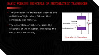
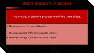
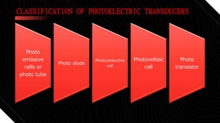
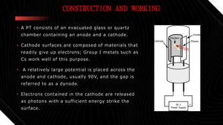
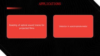
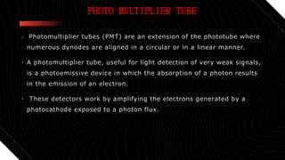
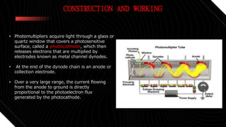
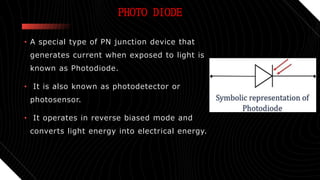
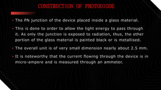
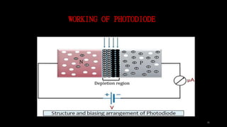
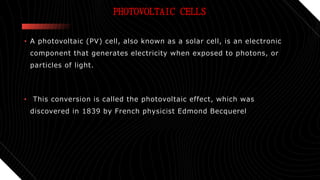
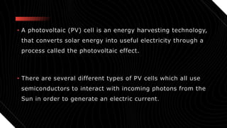
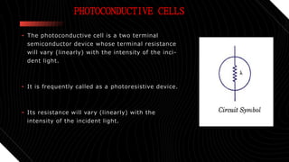
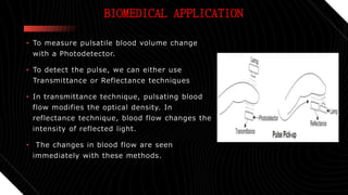
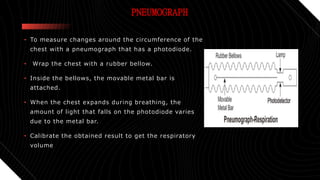
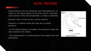
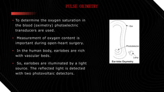
The photoelectric transducer converts the light energy into electrical energy. It is made of semiconductor material. The photoelectric transducer uses a photosensitive element, which ejects the electrons when the beam of light absorbs through it.
Types of Transducers
Analog and Digital Transducer
Characteristic of Transducer
Selection factor of Transducer
Measurement of Displacement
LVDT and RVDT
Different types of strain Gauges
Manometers
Pressure Measuring Elements
Hall Effect
Thermocouple
Types of Transducers
Analog and Digital Transducer
Characteristic of Transducer
Selection factor of Transducer
Measurement of Displacement
LVDT and RVDT
Different types of strain Gauges
Manometers
Pressure Measuring Elements
Hall Effect
Thermocouple
A photodiode is a semiconductor device that converts light into an electrical current. The current is generated when photons are absorbed in the photodiode. Photodiodes may contain optical filters, built-in lenses, and may have large or small surface areas.
EST 130, Transistor Biasing and Amplification.CKSunith1
The attached narrated power point presentation explains the need for biasing in transistor amplifiers and the different biasing arrangements used in transistor circuits. The material will be useful for KTU first year B Tech students who prepare for the subject EST 130, Part B, Basic Electronics Engineering.
An Auto Transformer is a transformer with only one winding wound on a laminated core. An auto transformer is similar to a two winding transformer but differ in the way the primary and secondary winding are interrelated. A part of the winding is common to both primary and secondary sides.
The Piezoelectric transducer is an electroacoustic transducer use for conversion of pressure or mechanical stress into an alternating electrical force. It is used for measuring the physical quantity like force, pressure, stress, etc., which is directly not possible to measure.The piezo transducer converts the physical quantity into an electrical voltage which is easily measured by analogue and digital meter.
The piezoelectric transducer uses the piezoelectric material which has a special property, i.e. the material induces voltage when the pressure or stress applied to it. The material which shows such property is known as the electro-resistive element
Permanent Magnet Moving Coil Instrument. The permanent magnet moving coil instrument or PMMC type instrument uses two permanent magnets in order to create stationary magnetic field.
In this u will study about
1.Working Principle
2.Parameter for CTT
3.Applications (in details)
4.Advantages
5.Disadvantages
of Capacitive Type Transducer
Presenting a topic which is entitled: Detectors
Above topic includes:
Types of detector
phototube detector
photomultiplier tubes
silicon photodiodes
photovoltaic cells
advantages
multi-channel photon detectors
linear photodiode arrays
photodiode array
with basics of instrumentation and science technology
https://www.linkedin.com/in/preeti-choudhary-266414182/
https://www.instagram.com/chaudharypreeti1997/
https://www.facebook.com/profile.php?id=100013419194533
https://twitter.com/preetic27018281
Please like, share, comment and follow.
stay connected
If any query then contact:
chaudharypreeti1997@gmail.com
Thanking-You
Preeti Choudhary
A p-n junction diode which emits spontaneous emission of radiation in the visible and IR regions when forward biased is called Light Emitting Diode.
This converts the input electrical energy into optical energy in the visible or IR spectrum depending on the semiconductor material
In thermogravimetric analysis, the change in weight in
relation to a change in temperature in a controlled environment is measured. Heat is used in TGA to force
reactions and physical changes in materials. Thermogravimetric analysis (TGA) is a reliable method to determine
endotherms, exotherms, measure oxidation processes, thermal stability, decomposition points of explosives,
characteristics of polymers, solvent residues, the level of organic and inorganic components of a mixture,
degradation temperatures of a material, and the absorbed moisture content of materials. Materials analyzed by
thermogravimetric analysis include explosives, petroleum, chemicals, biological samples, polymers, composites,
plastics, adhesives, coatings, organic materials, and pharmaceuticals.The thermogravimetric analysis instrument usually consists of a high-precision balance and sample pan.
The pan holds the sample
material and is located in a
furnace or oven that is
heated or cooled during the
experiment. A thermocouple
is used to accurately control
and measure the
temperature within the oven.
The mass of the sample is
constantly monitored during
the analysis. An inert or
reactive gas may be used to
purge and control the
environment. The analysis is
performed by gradually
raising the temperature and plotting the
substances weight against temperature. A
computer is utilized to control the
instrument and to process the output
curves.
Spectroscopy is the measurement and interpretation of electromagnetic radiation absorbed or emitted when the molecules or atoms or ions of a sample move from one energy state to another energy state. UV spectroscopy is a type of absorption spectroscopy in which light of the ultra-violet region (200-400 nm) is absorbed by the molecule which results in the excitation of the electrons from the ground state to a higher energy state.Basically, spectroscopy is related to the interaction of light with matter.
As light is absorbed by matter, the result is an increase in the energy content of the atoms or molecules.
When ultraviolet radiations are absorbed, this results in the excitation of the electrons from the ground state towards a higher energy state.
Molecules containing π-electrons or nonbonding electrons (n-electrons) can absorb energy in the form of ultraviolet light to excite these electrons to higher anti-bonding molecular orbitals.
The more easily excited the electrons, the longer the wavelength of light they can absorb. There are four possible types of transitions (π–π*, n–π*, σ–σ*, and n–σ*), and they can be ordered as follows: σ–σ* > n–σ* > π–π* > n–π* The absorption of ultraviolet light by a chemical compound will produce a distinct spectrum that aids in the identification of the compound.
Medical devices are heavily regulated because of their
intended uses in human beings. Generally medical devices
are classified into different categories depending upon the
degree of potential risks and regulated accordingly.Many medical devices are involved with relative moving parts,
either in contact to the native tissues or within the biomaterials,
and often under loading. Important issues, such as friction and
wear of the moving parts, not only affect the functions of these
devices but also the potential adverse effects on the natural tissues.
Biotribology deals with the application of tribological principles,
such as friction, wear and lubrication between relatively motions
surfaces, to medical and biological systems. Biotribology plays an important role in a number of medical devices
Protein based nanostructures for biomedical applications karoline Enoch
Proteins are kind of natural molecules that show unique
functionalities and properties in biological materials and
manufacturing feld. Tere are numerous nanomaterials
which are derived from protein, albumin, and gelatin. Tese
nanoparticles have promising properties like biodegradability, nonantigenicity, metabolizable, surface modifer, greater
stability during in vivo during storage, and being relatively
easy to prepare and monitor the size of the particles.
These particles have the ability to attach covalently with
drug and ligand
A Schering Bridge is a bridge circuit used for measuring an unknown electrical capacitance and its dissipation factor. The dissipation factor of a capacitor is the the ratio of its resistance to its capacitive reactance. The Schering Bridge is basically a four-arm alternating-current (AC) bridge circuit whose measurement depends on balancing the loads on its arms .
A Maxwell bridge is a modification to a Wheatstone bridge used to measure an unknown inductance (usually of low Q value) in terms of calibrated resistance and inductance or resistance and capacitance. When the calibrated components are a parallel resistor and capacitor, the bridge is known as a Maxwell-Wien bridge. It is named for James C. Maxwell, who first described it in 1873.
It uses the principle that the positive phase angle of an inductive impedance can be compensated by the negative phase angle of a capacitive impedance when put in the opposite arm and the circuit is at resonance; i.e., no potential difference across the detector (an AC voltmeter or ammeter)) and hence no current flowing through it. The unknown inductance then becomes known in terms of this capacitance.
A Kelvin bridge, also called a Kelvin double bridge and in some countries a Thomson bridge, is a measuring instrument used to measure unknown electrical resistors below 1 ohm. It is specifically designed to measure resistors that are constructed as four terminal resistors.
Dc bridge types ,derivation and its applicationkaroline Enoch
The DC Bridge is used for measuring the unknown electrical resistance. This can be done by balancing the two legs of the bridge circuit. The value of one of the arm is known while the other of them is unknown
The bridge uses for measuring the value of unknown resistance, inductance and capacitance, is known as the AC Bridge. The AC bridges are very convenient and give the accurate result of the measurement.The construction of the bridges is very simple. The bridge has four arms, one AC supply source and the balance detector. It works on the principle that the balance ratio of the impedances will give the balance condition to the circuit which is determined by the null detector.
Photodynamic therapy (PDT) is a two-stage treatment that combines light energy with a drug (photosensitizer) designed to destroy cancerous and precancerous cells after light activation. Photosensitizers are activated by a specific wavelength of light energy, usually from a laser.
Preamplifier and impedance matching circuitskaroline Enoch
A preamplifier circuit with a very low noise characteristic can be built by simply combining a FET transistor with a bipolar one. The input impedance of the preamp circuit is almost the same as the gate impedance of the FET transistor (around 1MΩ) The output impedance at the other end is about 1KΩ.
Phototherapy is a type of medical treatment that involves exposure to fluorescent light bulbs or other sources of light like halogen lights, sunlight, and light emitting diodes (LEDs) to treat certain medical conditions
The word “laser” is an acronym for light amplification by stimulated emission of radiation. Most sources of visible light radiate energy at different wavelengths (ie, different colors) and at random time intervals (noncoherent). The unique properties of laser energy are monochromaticity (single wavelength), spatial coherence, and high density of electrons. These allow focusing of laser beams to extremely small spots with very high-energy densities.
A laser consists of a transparent crystal rod (solid-state laser), or a gas- or liquid-filled cavity (gas or fluid laser) constructed with a fully reflective mirror at one end and a partially reflective mirror at the other. Surrounding the rod or cavity is an optical or electrical source of energy that will raise the energy level of the atoms within the rod or cavity to a high and unstable level, a process known as population inversion. When the excited atoms spontaneously decay back to a lower-energy level, their excess energy is released in the form of light. This light can be emitted in any direction. In a laser cavity, however, light emitted along the long axis of the cavity can bounce back and forth between the mirrors, setting up a standing wave that stimulates the remaining excited atoms to release their energy into the standing wave, producing an intense beam of light that exits the cavity through the partially reflective mirror. All of the light produced has the same wavelength (monochromatic) and phase (coherent), with little tendency to spread out (low divergence). The laser light energy can be emitted continuously or in pulses, which may have pulse durations of nanoseconds or less.
he ability of the laser to ablate prostatic tissue with minimal hemorrhage has concentrated most of the interest in urologically applied lasers to benign prostatic hyperplasia (BPH) [Anson et al. 1994]. Despite tremendous advances in the surgical and minimally invasive treatment of BPH, transurethral resection of the prostate (TURP) is still considered the ‘gold standard’. The risks of TURP are always mentioned when discussing the reasons for seeking alternative treatment modalities for BPH. Bleeding certainly remains a concern, especially in patients on some form of anticoagulation (heparin, coumarin related compounds, antiplatelet agents) or those with prostates in excess of 60–80 g. On the other hand, with the availability of transurethral resection in saline (TURiS), the TURP syndrome is nowadays considered by many to be a relatively rare complication
Lasers have been used successfully to treat a variety of vascular lesions including superficial vascular malformations (port-wine stains), facial telangiectases, haemangiomas, pyogenic granulomas, Kaposi sarcoma and poikiloderma of Civatte. Lasers that have been used to treat these conditions include argon, APTD, KTP, krypton, copper vapour, copper bromide, pulsed dye lasers and Nd:YAG. Argon (CW) causes a high degree of non-specific thermal injury and scarring and is now largely replaced by yellow-light quasi-CW and pulsed laser therapies.
The pulsed dye laser is considered the laser of choice for most vascular lesions because of its superior clinical efficacy and low-risk profile. It has a large spot size (5 to 10mm) allowing large lesions to be treated quickly. Side effects include postoperative bruising (purpura) that may last 1-2 weeks and transient pigmentary changes. Crusting, textural changes and scarring are rarely seen.
The term LASER is an acronym for ‘Light Amplification by the Stimulated Emission of Radiation’. As its first application in dentistry by Miaman, in 1960, the laser has seen various hard and soft tissue applications. In the last two decades, there has been an explosion of research studies in laser application. In hard tissue application, the laser is used for caries prevention, bleaching, restorative removal and curing, cavity preparation, dentinal hypersensitivity, growth modulation and for diagnostic purposes, whereas soft tissue application includes wound healing, removal of hyperplastic tissue to uncovering of impacted or partially erupted tooth, photodynamic therapy for malignancies, photostimulation of herpetic lesion. Use of the laser proved to be an effective tool to increase efficiency, specificity, ease, and cost and comfort of the dental treatment.
Photolithography, also called optical lithography or UV lithography, is a process used in microfabrication to pattern parts on a thin film or the bulk of a substrate (also called a wafer). It uses light to transfer a geometric pattern from a photomask (also called an optical mask) to a photosensitive (that is, light-sensitive) chemical photoresist on the substrate. A series of chemical treatments then either etches the exposure pattern into the material or enables deposition of a new material in the desired pattern upon the material underneath the photoresist. In complex integrated circuits, a CMOS wafer may go through the photolithographic cycle as many as 50 times.
Photolithography shares some fundamental principles with photography in that the pattern in the photoresist etching is created by exposing it to light, either directly (without using a mask) or with a projected image using a photomask. This procedure is comparable to a high precision version of the method used to make printed circuit boards. Subsequent stages in the process have more in common with etching than with lithographic printing. This method can create extremely small patterns, down to a few tens of nanometers in size. It provides precise control of the shape and size of the objects it creates and can create patterns over an entire surface cost-effectively. Its main disadvantages are that it requires a flat substrate to start with, it is not very effective at creating shapes that are not flat, and it can require extremely clean operating conditions. Photolithography is the standard method of printed circuit board (PCB) and microprocessor fabrication. Directed self-assembly is being evaluated as an alternative to photolithography
Piezoresistive pressure sensors are one of the very-first products of MEMS technology. Those products are widely used in biomedical applications, automotive industry and household appliances.
The sensing material in a piezoresistive pressure sensor is a diaphragm formed on a silicon substrate, which bends with applied pressure. A deformation occurs in the crystal lattice of the diaphragm because of that bending. This deformation causes a change in the band structure of the piezoresistors that are placed on the diaphragm, leading to a change in the resistivity of the material. This change can be an increase or a decrease according to the orientation of the resistors.
capacitive sensing (sometimes capacitance sensing) is a technology, based on capacitive coupling, that can detect and measure anything that is conductive or has a dielectric different from air. Many types of sensors use capacitive sensing, including sensors to detect and measure proximity, pressure, position and displacement, force, humidity, fluid level, and acceleration. Human interface devices based on capacitive sensing, such as trackpads, can replace the computer mouse. Digital audio players, mobile phones, and tablet computers use capacitive sensing touchscreens as input devices. Capacitive sensors can also replace mechanical buttons.
A capacitive touchscreen typically consists of a capacitive touch sensor along with at least two complementary metal-oxide-semiconductor (CMOS) integrated circuit (IC) chips, an application-specific integrated circuit (ASIC) controller and a digital signal processor (DSP). Capacitive sensing is commonly used for mobile multi-touch displays, popularized by Apple's iPhone in 2007.
apacitive sensors are constructed from many different media, such as copper, indium tin oxide (ITO) and printed ink. Copper capacitive sensors can be implemented on standard FR4 PCBs as well as on flexible material. ITO allows the capacitive sensor to be up to 90% transparent (for one layer solutions, such as touch phone screens). Size and spacing of the capacitive sensor are both very important to the sensor's performance. In addition to the size of the sensor, and its spacing relative to the ground plane, the type of ground plane used is very important. Since the parasitic capacitance of the sensor is related to the electric field's (e-field) path to ground, it is important to choose a ground plane that limits the concentration of e-field lines with no conductive object present.
Designing a capacitance sensing system requires first picking the type of sensing material (FR4, Flex, ITO, etc.). One also needs to understand the environment the device will operate in, such as the full operating temperature range, what radio frequencies are present and how the user will interact with the interface.
There are two types of capacitive sensing system: mutual capacitance,[5] where the object (finger, conductive stylus) alters the mutual coupling between row and column electrodes, which are scanned sequentially; and self- or absolute capacitance where the object (such as a finger) loads the sensor or increases the parasitic capacitance to ground. In both cases, the difference of a preceding absolute position from the present absolute position yields the relative motion of the object or finger during that time. The technologies are elaborated in the following section.
Pressure transducers and pressure sensors often consist of a spring element on which multiple strain gauges are installed. Hence, they work similarly to force transducers. A diaphragm is frequently used as the pressure-sensitive measuring body in the lower pressure range, while the spring element often consists of a single, tubular piece of steel in the high-pressure range.
Process pressure applies a mechanical load to the spring element, which experiences a deformation before returning to its original state. This deformation can be measured by strain gauges (SGs) and analyzed by measurement electronics.
Ideally, the strain gauges are installed in the area of greatest positive and negative strain or stress to obtain the highest possible SG sensitivity. Since the exact strain gradient and strain distribution in the measuring body are known at the pressure transducer's design stage, the shape, position, and length of the measuring grid can be optimized.
Cosmetic shop management system project report.pdfKamal Acharya
Buying new cosmetic products is difficult. It can even be scary for those who have sensitive skin and are prone to skin trouble. The information needed to alleviate this problem is on the back of each product, but it's thought to interpret those ingredient lists unless you have a background in chemistry.
Instead of buying and hoping for the best, we can use data science to help us predict which products may be good fits for us. It includes various function programs to do the above mentioned tasks.
Data file handling has been effectively used in the program.
The automated cosmetic shop management system should deal with the automation of general workflow and administration process of the shop. The main processes of the system focus on customer's request where the system is able to search the most appropriate products and deliver it to the customers. It should help the employees to quickly identify the list of cosmetic product that have reached the minimum quantity and also keep a track of expired date for each cosmetic product. It should help the employees to find the rack number in which the product is placed.It is also Faster and more efficient way.
Welcome to WIPAC Monthly the magazine brought to you by the LinkedIn Group Water Industry Process Automation & Control.
In this month's edition, along with this month's industry news to celebrate the 13 years since the group was created we have articles including
A case study of the used of Advanced Process Control at the Wastewater Treatment works at Lleida in Spain
A look back on an article on smart wastewater networks in order to see how the industry has measured up in the interim around the adoption of Digital Transformation in the Water Industry.
Water scarcity is the lack of fresh water resources to meet the standard water demand. There are two type of water scarcity. One is physical. The other is economic water scarcity.
Overview of the fundamental roles in Hydropower generation and the components involved in wider Electrical Engineering.
This paper presents the design and construction of hydroelectric dams from the hydrologist’s survey of the valley before construction, all aspects and involved disciplines, fluid dynamics, structural engineering, generation and mains frequency regulation to the very transmission of power through the network in the United Kingdom.
Author: Robbie Edward Sayers
Collaborators and co editors: Charlie Sims and Connor Healey.
(C) 2024 Robbie E. Sayers
Final project report on grocery store management system..pdfKamal Acharya
In today’s fast-changing business environment, it’s extremely important to be able to respond to client needs in the most effective and timely manner. If your customers wish to see your business online and have instant access to your products or services.
Online Grocery Store is an e-commerce website, which retails various grocery products. This project allows viewing various products available enables registered users to purchase desired products instantly using Paytm, UPI payment processor (Instant Pay) and also can place order by using Cash on Delivery (Pay Later) option. This project provides an easy access to Administrators and Managers to view orders placed using Pay Later and Instant Pay options.
In order to develop an e-commerce website, a number of Technologies must be studied and understood. These include multi-tiered architecture, server and client-side scripting techniques, implementation technologies, programming language (such as PHP, HTML, CSS, JavaScript) and MySQL relational databases. This is a project with the objective to develop a basic website where a consumer is provided with a shopping cart website and also to know about the technologies used to develop such a website.
This document will discuss each of the underlying technologies to create and implement an e- commerce website.
Student information management system project report ii.pdfKamal Acharya
Our project explains about the student management. This project mainly explains the various actions related to student details. This project shows some ease in adding, editing and deleting the student details. It also provides a less time consuming process for viewing, adding, editing and deleting the marks of the students.
2. PHOTOELECTRIC TRANSDUCER
• The photoelectric transducer converts the light energy into electrical
energy.
• It is made of semiconductor material.
• The photoelectric transducer uses a photosensitive element, which
ejects the electrons when the beam of light absorbs through it.
3. • The discharges of electrons vary the property of the photosensitive
element.
• Hence the current induces in the devices.
• The magnitude of the current is equal to the total light absorbed by
the photosensitive element.
4. BASIC WORKING PRINCIPLE OF PHOTOELCTRIC TRANSDUCER
• The photoelectric transducer absorbs the
radiation of light which falls on their
semiconductor material.
• The absorption of light energises the
electrons of the material, and hence the
electrons start moving.
5. EFFECTS OF MOBILITY OF ELECTRONS
The mobility of electrons produces one of the three effects.
• The resistance of the material changes.
• The output current of the semiconductor changes.
• The output voltage of the semiconductor changes.
6. CLASSIFICATION OF PHOTOELECTRIC TRANSDUCERS
Photo
emissive
cells or
photo tube
Photo diode
Photoconductive
cell
Photovoltaic
cell
Photo
transistor
7. PHOTO TUBES
• A phototube or photoelectric cell is a type of gas-filled or vacuum tube
that is sensitive to light.
• Such a tube is more correctly called a 'photoemissive cell' to
distinguish it from photovoltaic or photoconductive cells.
• Phototubes were previously more widely used but are now replaced in
many applications by solid state photodetectors.
8. PRINCIPLE
• Phototubes operate according to the photoelectric effect: Incoming
photons strike a photocathode, knocking electrons out of its surface,
which are attracted to an anode.
• Thus current is dependent on the frequency and intensity of incoming
photons.
9. CONSTRUCTION AND WORKING
• A PT consists of an evacuated glass or quartz
chamber containing an anode and a cathode.
• Cathode surfaces are composed of materials that
readily give up electrons; Group I metals such as
Cs work well of this purpose.
• A relatively large potential is placed across the
anode and cathode, usually 90V, and the gap is
referred to as a dynode.
• Electrons contained in the cathode are released
as photons with a sufficient energy strike the
surface.
10. • This causes electrons to move through the low-pressure gap to the
anode, which produces a current.
• For a PT, a single photon causes only a single electron to be
measured.
• For emission spectroscopy, the magnitude of current produced by the
cascade of electrons in the detector is directly proportional to the
concentration of analyte in the sample.
12. PHOTO MULTIPLIER TUBE
• Photomultiplier tubes (PMT) are an extension of the phototube where
numerous dynodes are aligned in a circular or in a linear manner.
• A photomultiplier tube, useful for light detection of very weak signals,
is a photoemissive device in which the absorption of a photon results
in the emission of an electron.
• These detectors work by amplifying the electrons generated by a
photocathode exposed to a photon flux.
13. CONSTRUCTION AND WORKING
• Photomultipliers acquire light through a glass or
quartz window that covers a photosensitive
surface, called a photocathode, which then
releases electrons that are multiplied by
electrodes known as metal channel dynodes.
• At the end of the dynode chain is an anode or
collection electrode.
• Over a very large range, the current flowing
from the anode to ground is directly
proportional to the photoelectron flux
generated by the photocathode.
14. • The spectral response, quantum efficiency, sensitivity, and dark current of a
photomultiplier tube are determined by the composition of the photocathode.
• The best photocathodes capable of responding to visible light are less than
30 percent quantum efficient, meaning that 70 percent of the photons
impacting on the photocathode do not produce a photoelectron and are
therefore not detected.
• Photocathode thickness is an important variable that must be monitored to
ensure the proper response from absorbed photons.
• If the photocathode is too thick, more photons will be absorbed but fewer
electrons will be emitted from the back surface, but if it is too thin, too
many photons will pass through without being absorbed.
15. • Electrons emitted by the photocathode are
accelerated toward the dynode chain, which may
contain up to 14 elements.
• Focusing electrodes are usually present to ensure
that photoelectrons emitted near the edges of the
photocathode will be likely to land on the first
dynode.
• Upon impacting the first dynode, a photoelectron
will invoke the release of additional electron that
are accelerated toward the next dynode, and so
on.
16. • The surface composition and geometry of the dynodes determines their ability to
serve as electron multipliers
• Because gain varies with the voltage across the dynodes and the total number of
dynodes, electron gains of 10 million are possible if 12-14 dynode stages are
employed.
• Photomultipliers produce a signal even in the absence of light due to dark
current arising from thermal emissions of electrons from the photocathode,
leakage current between dynodes, as well as stray high-energy radiation.
• Electronic noise also contributes to the dark current and is often included in the
dark-current value.
17. APPLICATIONS
• Photomultipliers are used in research laboratories to measure the intensity
and spectrum of light-emitting materials such as compound semiconductors
and quantum dots.
• Photomultipliers are used as the detector in many spectrophotometers.
18. • A special type of PN junction device that
generates current when exposed to light is
known as Photodiode.
• It is also known as photodetector or
photosensor.
• It operates in reverse biased mode and
converts light energy into electrical energy.
PHOTO DIODE
19. CONSTRUCTION OF PHOTODIODE
• The PN junction of the device placed inside a glass material.
• This is done to order to allow the light energy to pass through
it. As only the junction is exposed to radiation, thus, the other
portion of the glass material is painted black or is metallised.
• The overall unit is of very small dimension nearly about 2.5 mm.
• It is noteworthy that the current flowing through the device is in
micro-ampere and is measured through an ammeter.
20. OPERATIONAL MODES OF PHOTODIODE
Photodiode basically operates in two modes:
Photovoltaic mode: It is also known as zero-bias mode because no
external reverse potential is provided to the device. However, the flow of
minority carrier will take place when the device is exposed to light.
Photoconductive mode: When a certain reverse potential is applied to the
device then it behaves as a photoconductive device. Here, an increase in
depletion width is seen with the corresponding change in reverse voltage.
22. WORKING OF PHOTODIODE
• In the photodiode, a very small reverse current flows through the device
that is termed as dark current.
• It is called so because this current is totally the result of the flow of
minority carriers and is thus flows when the device is not exposed to
radiation.
• The electrons present in the p side and holes present in n side are the
minority carriers.
• When a certain reverse-biased voltage is applied then minority carrier, holes
from n-side experiences repulsive force from the positive potential of the
battery
23. Contd..
• Similarly, the electrons present in the p side experience repulsion
from the negative potential of the battery.
• Due to this movement electron and hole recombine at the junction
resultantly generating depletion region at the junction.
• Due to this movement, a very small reverse current flows through the
device known as dark current.
• The combination of electron and hole at the junction generates neutral
atom at the depletion. Due to which any further flow of current is
restricted.
24. Contd..
• Now, the junction of the device is illuminated with light. As the
light falls on the surface of the junction, then the temperature
of the junction gets increased. This causes the electron and hole
to get separated from each other.
• At the two gets separated then electrons from n side gets
attracted towards the positive potential of the battery. Similarly,
holes present in the p side get attracted to the negative
potential of the battery.
25. Contd..
• This movement then generates high reverse current
through the device.
• With the rise in the light intensity, more charge carriers are
generated and flow through the device. Thereby, producing
a large electric current through the device.
• This current is then used to drive other circuits of the
system
26. Contd..
• The intensity of light energy is directly
proportional to the current through the
device.
• Only positive biased potential can put
the device in no current condition in
case of the photodiode
27. Contd..
• Here, the vertical line represents the
reverse current flowing through the
device and the horizontal line represents
the reverse-biased potential.
• The first curve represents the dark
current that generates due to minority
carriers in the absence of light.
• all the curve shows almost equal spacing
in between them. This is so because
current proportionally increases with the
luminous flux.
28. ADVANTAGES OF PHOTODIODE
It shows a
quick response
when exposed
to light.
High
operational
speed.
It provides a
linear
response.
Low-cost
device
29. DISADVANTAGES OF PHOTODIODE
It is a temperature-dependent device. And shows poor temperature
stability.
When low illumination is provided, then amplification is necessary.
30. APPLICATION OF PHOTODIODE
Counters and
switching
circuits.
optical
communication
system.
Logic circuits
and encoders.
Burglar alarm
systems.
31. PHOTOVOLTAIC CELLS
• A photovoltaic (PV) cell, also known as a solar cell, is an electronic
component that generates electricity when exposed to photons, or
particles of light.
• This conversion is called the photovoltaic effect, which was
discovered in 1839 by French physicist Edmond Becquerel
32. • A photovoltaic (PV) cell is an energy harvesting technology,
that converts solar energy into useful electricity through a
process called the photovoltaic effect.
• There are several different types of PV cells which all use
semiconductors to interact with incoming photons from the
Sun in order to generate an electric current.
33. PRINCIPLE
• The photovoltaic effect is a process that generates voltage or
electric current in a photovoltaic cell when it is exposed to
sunlight.
• The photovoltaic effect can be defined as being the appearance
of a potential difference (voltage) between two layers of a
semiconductor slice in which the conductivities are opposite, or
between a semiconductor and a metal, under the effect of a
light stream.
34. CONSTRUCTION OF PHOTOVOLTAIC CELLS
• A photovoltaic cell is made of
semiconductor materials that absorb the
photons emitted by the sun and generate a
flow of electrons.
• Photons are elementary particles that
carry solar radiation at a speed of 300,000
kilometers per second.
• In the 1920s, Albert Einstein referred to
them as “grains of light”. When the photons
strike a semiconductor material like silicon
, they release the electrons from its atoms,
leaving behind a vacant space
35. • The stray electrons move around randomly looking for another “hole”
to fill.
• To produce an electric current, however, the electrons need to flow in
the same direction.
• This is achieved using two types of silicon.
• The silicon layer that is exposed to the sun is doped with atoms of
phosphorus, which has one more electron than silicon, while the other
side is doped with atoms of boron , which has one less electron.
36. • On either side of the semiconductor is a layer of conducting
material which "collects" the electricity produced.
• Note that the backside or shaded side of the cell can afford to
be completely covered in the conductor, whereas the front or
illuminated side must use the conductors sparingly to avoid
blocking too much of the Sun's radiation from reaching the
semiconductor.
• The final layer which is applied only to the illuminated side of
the cell is the anti-reflection coating.
37. • Since all semiconductors are naturally reflective, reflection loss can be
significant.
• The solution is to use one or several layers of an anti-reflection
coating (similar to those used for eyeglasses and cameras) to reduce
the amount of solar radiation that is reflected off the surface of the
cell
38. WORKING OF PHOTOVOLTAIC CELLS
• These solar cells are composed of two
different types of semiconductors—a p-
type and an n-type—that are joined
together to create a p-n junction.
• By joining these two types of
semiconductors, an electric field is
formed in the region of the junction as
electrons move to the positive p-side
and holes move to the negative n-side.
• This field causes negatively charged
particles to move in one direction and
positively charged particles in the other
direction.
39. • Light is composed of photons, which are simply small bundles of
electromagnetic radiation or energy.
• When light of a suitable wavelength is incident on these cells, energy from
the photon is transferred to an electron of the semiconducting material,
causing it to jump to a higher energy state known as the conduction band.
• In their excited state in the conduction band, these electrons are free to
move through the material, and it is this motion of the electron that creates
an electric current in the cell.
40. • Efficiency is a design concern for photovoltaic cells, as there are many
factors that limit their efficiency.
• The main factor is that 1/4 of the solar energy to the Earth cannot be
converted into electricity by a silicon semiconductor.
• The physics of semiconductors requires a minimum photon energy to remove
an electron from a crystal structure, known as the band-gap energy.
• If a photon has less energy than the band-gap, the photon gets absorbed as
thermal energy. For silicon, the band-gap energy is 1.12 electron volts.
41. • Since the energy in the photons from the sun cover a wide range of
energies, some of the incoming energy from the Sun does not have
enough energy to knock off an electron in a silicon PV cell.
• Even from the light that can be absorbed, there is still a problem.
Any energy above the band-gap energy will be transformed into heat.
• This also cuts the efficiency because that heat energy is not being
used for any useful task.
•
42. • Of the electrons that are made available, not all of them will
actually make it to the metal contact and generate electricity.
• This is because some of them will not be accelerated
sufficiently by the voltage inside the semiconductor.
• Because of the reasons listed, the theoretical efficiency of
silicon PV cells is about 33%
• .
43. • There are ways to improve the efficiency of PV cells, all of which come
with an increased cost.
• Some of these methods include increasing the purity of the
semiconductor, using a more efficient semiconducting material such as
Gallium Arsenide, by adding additional layers or p-n junctions to the cell,
or by concentrating the Sun's energy using concentrated photovoltaics.
• On the other hand, PV cells will also degrade, outputting less energy
over time, due to a variety of factors including UV exposure and weather
cycles.
44. DIFFERENT TYPES OF PHOTOVOLTAIC CELLS
Crystalline
Silicon Cells
Thin-Film
Cells
Organic Cells Perovskites
45. PHOTOCONDUCTIVE CELLS
• The photoconductive cell is a two terminal
semiconductor device whose terminal resistance
will vary (linearly) with the intensity of the inci-
dent light.
• It is frequently called as a photoresistive device.
• Its resistance will vary (linearly) with the
intensity of the incident light.
46. PRINCIPLE
• Light striking the surface of a material can provide sufficient energy
to cause electrons within the material to break away from their
atoms.
• Thus, free electrons and holes (charge carriers) are created within
the material, and consequently its resistance is reduced.
• This is known as the Photoconductive effect.
47. CONSTRUCTION AND WORKING
• Light-sensitive material is arranged in the form of a long strip
zigzagged across a disc-shaped base.
• The connecting terminals are fitted to the conducting material
on each side of the strip; they are not at the ends of the strip.
• Thus, the light sensitive material is actually a short, wide strip
between the two conductors.
• For added protection, a transparent plastic cover is usually
included
48. • Cadmium sulfide (CdS) and cadmium selenide (CdSe) are the two
materials normally used in photoconductive cell manufacture.
• Both respond rather slowly to changes in light intensity.
• For cadmium selenide, the response time (tres) is around 10 ms,
while for cadmium sulfide it may be as long as 100 ms.
• Temperature sensitivity is another important difference between the
two materials
49. • There is a large change in the resistance of a cadmium selenide cell with
changes in ambient temperature, but the resistance of cadmium sulfide
remains relatively stable.
• As with all other devices, care must be taken to ensure that the power
dissipation is not excessive.
• The spectral response of a cadmium sulfide cell is similar to that of the
human eye; it responds to visible light.
• For a cadmium selenide cell, the spectral response is at the longer
wavelength end of the visible spectrum and extends into the infrared region.
50. CHARACTERISTICS OF PHOTOCONDUCTIVE CELL
• The illumination characteristics of a typical
photoconductive cell are in figure.
• Initially the cell is not lit up.
• At that time its resistance can be more than 10
kilo-ohm.
• This resistance is the dark resistance.
• When the cell is lit up. Now the resistance may
fall to few hundred ohms.
• Cell sensitivity is expressed in terms of cell
current, input voltage and input level of
illumination
51. APPLICATIONS OF PHOTOCONDUCTIVE CELL
• The photoconductive cell used for relay
control. When the cell is lit up.
• Then its resistance is less and the relay
current is at its maximum.
• When the cell is dark, its high resistance
reduces the current down to a level too low
to energize the relay.
• Resistance R is to limit the relay current to
desired level when the resistance of the cell
is low.
52. DRAWBACKS
• Temperature variations cause substantial variations in resistance for a
particular light intensity.
• Unsuitable for analog applications.
53. PHOTO TRANSISTOR
• Phototransistor is an electronic switching and current amplification
component which relies on exposure to light to operate.
• When light falls on the junction, reverse current flows which are proportional
to the luminance.
• Phototransistors are used extensively to detect light pulses and convert
them into digital electrical signals.
• These are operated by light rather than electric current.
• Providing a large amount of gain, low cost and these phototransistors might
be used in numerous applications
54. • It is capable of converting light energy into electric energy.
• Phototransistors work in a similar way to photoresistors commonly known as LDR
(light dependent resistor) but are able to produce both current and voltage while
photoresistors are only capable of producing current due to change in resistance.
• Phototransistors are transistors with the base terminal exposed.
• Instead of sending current into the base, the photons from striking light activate
the transistor.
• This is because a phototransistor is made of a bipolar semiconductor and focuses the
energy that is passed through it.
• These are activated by light particles and are used in virtually all electronic devices
that depend on light in some way.
55. CHARACTERISTICS
Low-cost visible and near-IR photodetection.
Available with gains from 100 to over 1500.
Moderately fast response times.
Available in a wide range of packages including epoxy-coated, transfer-molded and surface
mounting technology.
Electrical characteristics were similar to that of signal transistors.
56. CONSTRUCTION OF PHOTOTRANSISTOR
• A phototransistor is nothing but an ordinary bi-polar
transistor in which the base region is exposed to the
illumination.
• It is available in both the P-N-P and N-P-N types
having different configurations like common emitter,
common collector and common base.
• Common emitter configuration is generally used.
• It can also work while the base is made open.
Compared to the conventional transistor it has more
base and collector areas..
57. • Ancient phototransistors used single semiconductor materials like silicon and
germanium but now a day’s modern components use materials like gallium
and arsenide for high-efficiency levels.
• The base is the lead responsible for activating the transistor. It is the gate
controller device for the larger electrical supply.
• The collector is the positive lead and the larger electrical supply.
• The emitter is the negative lead and the outlet for the larger electrical
supply
58. • With no light falling on the device there will be a small current flow due to
thermally generated hole-electron pairs and the output voltage from the
circuit will be slightly less than the supply value due to the voltage drop
across the load resistor R.
• With light falling on the collector-base junction the current flow increases.
• With the base connection open circuit, the collector-base current must flow
in the base-emitter circuit and hence the current flowing is amplified by
normal transistor action.
59. • The collector-base junction is very sensitive to light.
• Its working condition depends upon the intensity of light.
• The base current from the incident photons is amplified by the gain of
the transistor, resulting in current gains that range from hundreds to
several thousand.
• A phototransistor is 50 to 100 times more sensitive than a photodiode
with a lower level of noise
60. PHOTOTRANSISTOR CIRCUIT
• A phototransistor works just like a normal transistor, where the base current is multiplied
to give the collector current, except that in a phototransistor, the base current is
controlled by the amount of visible or infrared light where the device only needs 2 pins.
61. • In the simple circuit, assuming that nothing is connected to Vout, the
base current controlled by the amount of light will determine the
collector current, which is the current going through the resistor.
• Therefore, the voltage at Vout will move high and low based on the
amount of light.
• The output of a phototransistor is dependent upon the wavelength of
the incident light.
62. • These devices respond to light over a broad range of wavelengths
from the near UV, through the visible and into the near IR part of the
spectrum.
• For a given light source illumination level, the output of a
phototransistor is defined by the area of the exposed collector-base
junction and the dc current gain of the transistor
63. • Phototransistors available different configurations like optoisolator, optical
switch, retro sensor.
• Optoisolator is similar to a transformer in that the output is electrically
isolated from the input.
• An object is detected when it enters the gap of the optical switch and blocks
the light path between the emitter and detector.
• The retro sensor detects the presence of an object by generating light and
then looking for its reflectance off of the object to be sensed.
64. ADVANTAGES OF PHOTOTRANSISTOR
• Phototransistors produce higher current than photodiodes.
• Phototransistors are relatively inexpensive, simple, and small enough
to fit several of them onto a single integrated computer chip.
• Phototransistors are very fast and are capable of providing nearly
instantaneous output.
• Phototransistors produce a voltage, that photo-resistors cannot do so.
65. DISADVANTAGES OF PHOTOTRANSISTOR
• Phototransistors that are made of silicon are not capable of
handling voltages over 1,000 Volts.
• Phototransistors are also more vulnerable to surges and spikes of
electricity as well as electromagnetic energy.
• Phototransistors also do not allow electrons to move as freely as other
devices do, such as electron tubes.
67. BIOMEDICAL APPLICATION
• To measure pulsatile blood volume change
with a Photodetector.
• To detect the pulse, we can either use
Transmittance or Reflectance techniques
• In transmittance technique, pulsating blood
flow modifies the optical density. In
reflectance technique, blood flow changes the
intensity of reflected light.
• The changes in blood flow are seen
immediately with these methods.
68. PNEUMOGRAPH
• To measure changes around the circumference of the
chest with a pneumograph that has a photodiode.
• Wrap the chest with a rubber bellow.
• Inside the bellows, the movable metal bar is
attached.
• When the chest expands during breathing, the
amount of light that falls on the photodiode varies
due to the metal bar.
• Calibrate the obtained result to get the respiratory
volume
69. BLOOD PRESSURE
• Blood pressure can be measured with Photodetectors as
shown in the figure below. At the free end of a bourdon
tube between lamp and photodiode, a shade is attached.
• Bourdon tube is filled using a saline solution.
• Pressure is created inside the tube due to blood
pressure.
• As the blood pressure increases, the pressure inside the
tube displaces the shade.
• This displacement is proportional to the output from the
phototube.
70. PULSE OXIMETRY
• To determine the oxygen saturation in
the blood (oximetry) photoelectric
transducers are used.
• Measurement of oxygen content is
important during open-heart surgery.
• In the human body, earlobes are rich
with vascular beds.
• So, earlobes are illuminated by a light
source. The reflected light is detected
with two photovoltaic detectors.
71. • The first detector detects the emitted radiation in the red region (640mµ),
and another detector detects in the IR region (800mµ).
• The output from the red channel is related to the oxygen content in blood
and the presence of blood and tissue along the optical path.
• However, the output from the IR spectrum is not proportional to the oxygen
saturation.
• Finally, the difference between the two outputs is proportional to the
amount of oxygen present in the blood.