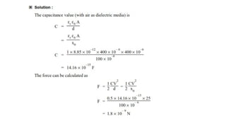
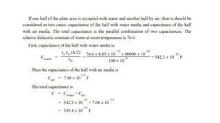
MEMS or MicroElectro Mechanical Systems, is a technology can be defined as
electromechanical and miniaturized mechanical elements that are manufactured
using the microfabrication techniques.
Its physical dimensions can be varied from sub-micron level to several
millimetres. MEMS devices comprises of both moving and non-moving
elements.
Usually non-moving elements will have simple structures and the moving
elements may have extremely complex structures.
MEMS has an interdisciplinary nature and uses the design, engineering and
manufacturing knowledge from a wide range of technical areas including IC
fabrication technology, mechanical engineering, materials science, electrical
engineering, chemistry and chemical engineering and its sub technological
fields.
3.
MEMS hasits unique applications in systems ranging across medical, automobiles, electrical,
communication, electronics and defence applications.
Current MEMS devices include inkjet printer heads, airbag sensors, projection display chips, computer
disk drive heads, pressure sensors, optical switches, biosensors, microvalves and many products that are
all manufactured and shipped commercially in high volumes.
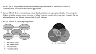
MEMS consists of following components:
1. Microstructures
2 Microelectronics
3. Microsensors
4. Microactuators
4.
There are threemajor merits for MEMS devices and microfabrication technology:
1. Miniaturization
2. Microelectronics integration
3. Parallel fabrication
MEMS products will compete in the market for its unique advantages like fast speed, functional surety, size
capabilities and lower cost.
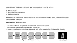
Introduction to Microfabrication
MEMS and IC devices are generally made on single crystal silicon wafers.
The below flow diagram denotes the flow of the process.
It explains overall process from the production of such wafers to packaging of individual device chips
Crystal seed
5.
• Bulk siliconwith crystalline consistency does not exist in nature and must be prepared through
laborious industrial processes.
• To make bulk crystal silicon, one starts with a perfect single crystal silicon seed.
• It is dipped into a molten silicon pool and slowly drawn out of the liquid.
• Silicon crystallizes when drawn into the atmosphere and establishes crystallinity consistent with that
of the initial seed.
• Rods of single crystal with various diameters and longitudinal crystal orientation can be formed this
way. The rods are sawed into thin, circular slices and polished to form wafers.
• After polishing, the wafer goes through a multistep fabrication process and packed as a complete
package.
Photolithography
Fabrication Process
The goal of photolithography is to produce fine features on wafer surfaces.
• A most common lithography process involves depositing photo-sensitive chemicals (called
photoresists, or simply resists) on a silicon wafer, exposing it with light through a mask and
removing (develop) photoresist material that has been modified by light.
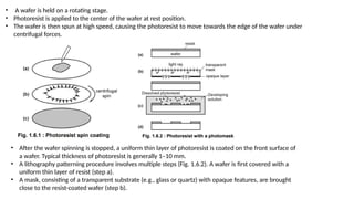
• The starting point of a lithography process is to coat a wafer with photoresist through spin
coating (Fig. 1.6.1)
6.
• A waferis held on a rotating stage.
• Photoresist is applied to the center of the wafer at rest position.
• The wafer is then spun at high speed, causing the photoresist to move towards the edge of the wafer under
centrifugal forces.
• After the wafer spinning is stopped, a uniform thin layer of photoresist is coated on the front surface of
a wafer. Typical thickness of photoresist is generally 1–10 mm.
• A lithography patterning procedure involves multiple steps (Fig. 1.6.2). A wafer is first covered with a
uniform thin layer of resist (step a).
• A mask, consisting of a transparent substrate (e.g., glass or quartz) with opaque features, are brought
close to the resist-coated wafer (step b).
7.
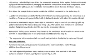
• High energy,collimated light rays strikes the mask-wafer assembly. Resist regions that are not covered
by opaque features are exposed, changing the chemical composition of the resist. For positive resist,
the exposure by light causes the resist to be more soluble in a wet chemical developer (step c).
• This allows the opaque features on the mask to be faithfully transferred to the wafer (step d).
• A pattern in photoresist can be further transferred to an underlying layer, using the photoresist as a
mask layer. The process is shown in Fig. 1.6.3. It starts with a wafer with a thin film coating (step a).
• The wafer is covered with a spin-coated layer of photoresist (step b), which is photolithographically
patterned similar to the method discussed in Fig. 1.6.2. The wafer is then immersed in a chemical
solution that preferably etch the thin film but not the photoresist (step c).
• With proper timing control, the thin film covered by the photoresist would stay intact, whereas the
thin film in areas not covered by the photoresist would be removed (step d).
• The photoresist is then preferentially removed, leaving the thin film behind as patterned (step e).
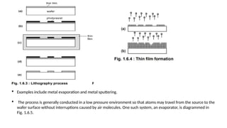
Thin Film Deposition
• Functional materials, conductors and insulators can be incorporated on a wafer through
additive deposition process.
• One such deposition process is direct transfer of the material from a source to the wafer
surface in an atom-by-atom, layer-by-layer fashion (Fig. 1.6.4).
8.
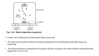
Examples includemetal evaporation and metal sputtering.
The process is generally conducted in a low pressure environment so that atoms may travel from the source to the
wafer surface without interruptions caused by air molecules. One such system, an evaporator, is diagrammed in
Fig. 1.6.5.
9.
• A waferand a metal source are both placed inside a vacuum jar.
• The metal can be transferred either by heating it (evaporation) or by bombarding it with high-energy ions
(sputtering).
• The achieved thickness is proportional to the power and time. In practice, the routine thickness of metal thin films
ranges from 1 nm to 2 mm.
10.
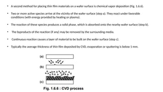
• A secondmethod for placing thin film materials on a wafer surface is chemical vapor deposition (Fig. 1.6.6).
• Two or more active species arrive at the vicinity of the wafer surface (step a). They react under favorable
conditions (with energy provided by heating or plasma).
• The reaction of these species produces a solid phase, which is absorbed onto the nearby wafer surface (step b).
• The byproducts of the reaction (if any) may be removed by the surrounding media.
• Continuous reaction causes a layer of material to be built on the wafer surface (step c).
• Typically the average thickness of thin film deposited by CVD, evaporation or sputtering is below 1 mm.
11.
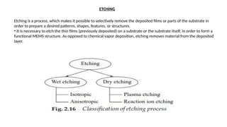
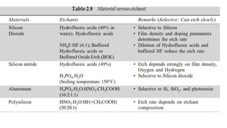
ETCHING
Etching is aprocess, which makes it possible to selectively remove the deposited films or parts of the substrate in
order to prepare a desired patterns, shapes, features, or structures.
• It is necessary to etch the thin films (previously deposited) on a substrate or the substrate itself, in order to form a
functional MEMS structure. As opposed to chemical vapor deposition, etching removes material from the deposited
layer.
12.
Two classes ofetching process are common. They are wet etching and dry etching.
• Wet etching removes the material selectively through chemical reaction. The material is immersed in a chemical
solution, which reacts and subsequently dissolves
the portion of the material, which is in contact with the solution. Materials not covered by the masks are etched away
by the chemical solutions while those covered by the masks are left undissolved.
• On the other hand, dry etching sputter the material using reactive ions or a vapor etchant. Each etching process is
further classified as shown in Fig. 2.16.
Wet Etching
Wet etching is the simplest method. It is important to note that the liquid solvent should not change the chemical
properties of the dissolved material such as photoresist, SiO2
, etc. Sometimes the wet etching process involves more than one chemical reaction and is, in fact, applicable only to
multi-layer structures which require sequential etching.
13.
The etchant isusually a mixture of acidic solutions. The selectivity of the etchant plays a major role in wet
etching. Selectivity refers to how effectively the etchant reacts with the material without corrugating other
materials deposited in the structure for other purposes (anchor, posts, etc.). An etchant may attack the mask
or the substrate itself making significant changes in the etching profile,
which is not desired. So appropriate combination of etchant, mask material and substrate are to be selected
prior to fabrication in order to obtain good results. The sequence of operations within the wet etching process
fall under three sub-activities:
• Diffusion of the etchant to the surface for removal. The operation is carried out at room temperature or
slightly above, but preferably below 50°C.
• Establishment of reaction between the etchant and the material being removed.
• Diffusion of the reaction by products from the reacted surface. This activity can also be called cleaning.
15.
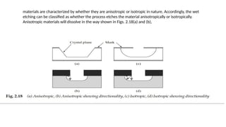
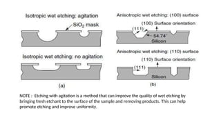
materials are characterizedby whether they are anisotropic or isotropic in nature. Accordingly, the wet
etching can be classified as whether the process etches the material anisotropically or isotropically.
Anisotropic materials will dissolve in the way shown in Figs. 2.18(a) and (b),
16.
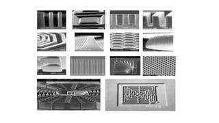
MEMS structure mayrequire anisotropic or isotropic etching. Rectangular (or square) cavities,
hemispheres, cylinders and mesas are achievable on the (100) substrate through wet anisotropic etching.
Anisotropic etching is useful in producing grooves, pyramids, and channels into the surface of the wafer.
Given a specific material the etchant can also be selected to etch the material either isotropically or
anisotropically. If it is required to fabricate holes of conical structure, i.e. Wider towards the top and
narrower toward the bottom on the crystalline silicon, then anisotropic etching will be obvious choice and
we have to look for anisotropic etchants like alkaline chemicals.
19.
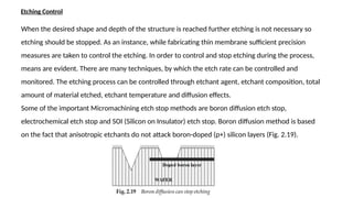
Etching Control
When thedesired shape and depth of the structure is reached further etching is not necessary so
etching should be stopped. As an instance, while fabricating thin membrane sufficient precision
measures are taken to control the etching. In order to control and stop etching during the process,
means are evident. There are many techniques, by which the etch rate can be controlled and
monitored. The etching process can be controlled through etchant agent, etchant composition, total
amount of material etched, etchant temperature and diffusion effects.
Some of the important Micromachining etch stop methods are boron diffusion etch stop,
electrochemical etch stop and SOI (Silicon on Insulator) etch stop. Boron diffusion method is based
on the fact that anisotropic etchants do not attack boron-doped (p+) silicon layers (Fig. 2.19).
20.
Material, from whichthe MEMS structures will be obtained, doped with both boron and germanium, for example,
can be etched much slower than undoped silicon. Boron p+ is diffused from the back of the substrate before the
anisotropic etching is performed. Electrochemical technique uses lightly doped p-n junction (being the wafer) as
cathode and a counter electrode as anode in the etchant KOH. The bias voltage is applied between the wafer and
anode. The wafer is immersed in the solution. In this process a p-type substrate can be etched and stopped at the p-
n junction. Another etch-stop technique is employed in terms of a change in composition of material. As an example
a layer of silicon dioxide between two layers of silicon can facilitate etching control due to the reason that many
etchants of silicon do not react with silicon dioxide. The method is based on SOI etch stop.
21.
MICRO MACHINING
BULK MICROMACHINING:
Machiningis defined as the process of removing material from a work piece in the form of chips in
order to obtain the exact shape and size of the work piece required.
Micro maching is considered as a process as well as technology that is utilized to structure wafer
materials or thin films in order to fabricate miniature devices such as micro sensors, micro actuators
and passive components ( electronic amplifier, bridge circuits, gear etc) for microsystems functioning
as electromechanical, opto electronic and opto mechanical systems.
Bulk micromachining technique was developed in 1960s and allows the selective removal of significant
amounts of silicon from a substrate to form membranes on one side of a wafer, a variety of trenches,
holes, or other structures . The bulk micromachining technique can be divided into wet etching and dry
etching of silicon according to the phase of etchants. Liquid etchants, almost exclusively relying on
aqueous chemicals, are referred to as wet etching, while vapor and plasma etchants are referred to as
dry etching.
22.
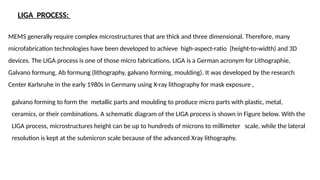
NOTE : Etchingwith agitation is a method that can improve the quality of wet etching by
bringing fresh etchant to the surface of the sample and removing products. This can help
promote etching and improve uniformity.
23.
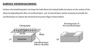
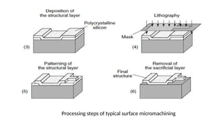
SURFACE MICROMACHINING:
Surface micromachiningdoes not shape the bulk silicon but instead builds structures on the surface of the
silicon by depositing thin films of sacrificial layers and structural layers and by removing eventually the
sacrificial layers to release the mechanical structures (figure shown below)
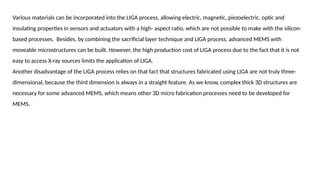
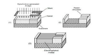
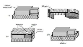
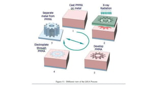
LIGA PROCESS:
MEMS generallyrequire complex microstructures that are thick and three dimensional. Therefore, many
microfabrication technologies have been developed to achieve high-aspect-ratio (height-to-width) and 3D
devices. The LIGA process is one of those micro fabrications. LIGA is a German acronym for Lithographie,
Galvano formung, Ab formung (lithography, galvano forming, moulding). It was developed by the research
Center Karlsruhe in the early 1980s in Germany using X-ray lithography for mask exposure ,
galvano forming to form the metallic parts and moulding to produce micro parts with plastic, metal,
ceramics, or their combinations. A schematic diagram of the LIGA process is shown in Figure below. With the
LIGA process, microstructures height can be up to hundreds of microns to millimeter scale, while the lateral
resolution is kept at the submicron scale because of the advanced Xray lithography.
26.
Various materials canbe incorporated into the LIGA process, allowing electric, magnetic, piezoelectric, optic and
insulating properties in sensors and actuators with a high- aspect ratio, which are not possible to make with the silicon-
based processes. Besides, by combining the sacrificial layer technique and LIGA process, advanced MEMS with
moveable microstructures can be built. However, the high production cost of LIGA process due to the fact that it is not
easy to access X-ray sources limits the application of LIGA.
Another disadvantage of the LIGA process relies on that fact that structures fabricated using LIGA are not truly three-
dimensional, because the third dimension is always in a straight feature. As we know, complex thick 3D structures are
necessary for some advanced MEMS, which means other 3D micro fabrication processes need to be developed for
MEMS.
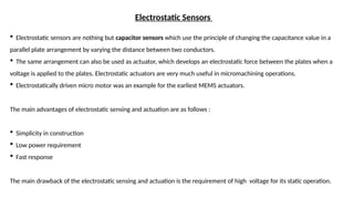
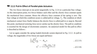
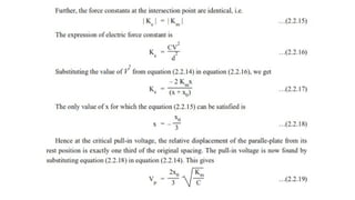
Electrostatic Sensors
Electrostaticsensors are nothing but capacitor sensors which use the principle of changing the capacitance value in a
parallel plate arrangement by varying the distance between two conductors.
The same arrangement can also be used as actuator, which develops an electrostatic force between the plates when a
voltage is applied to the plates. Electrostatic actuators are very much useful in micromachining operations.
Electrostatically driven micro motor was an example for the earliest MEMS actuators.
The main advantages of electrostatic sensing and actuation are as follows :
Simplicity in construction
Low power requirement
Fast response
The main drawback of the electrostatic sensing and actuation is the requirement of high voltage for its static operation.
32.
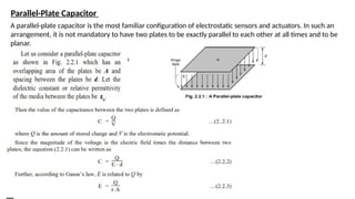
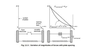
Parallel-Plate Capacitor
A parallel-platecapacitor is the most familiar configuration of electrostatic sensors and actuators. In such an
arrangement, it is not mandatory to have two plates to be exactly parallel to each other at all times and to be
planar.
33.
From the equation(2.2.4), it is observed that the capacitance is a function of A, d and Ɛ
Ɛ, A or d can be sensed by measuring the capacitance value of a parallel-plate capacitor. The change in capacitance
with change in permittivity can be used to characterize liquid, air or any biological particles in the gap. Similarly, the
change in capacitance with change in either overlapping area of or spacing between the plates can be used in the
measurement of contact force, static pressure, dynamic pressure and acceleration. In a parallel-plate capacitor, the
plates can be moved in two ways: normal displacement and Parallel sliding movement.
44.
Electro-mechanical systems
In somegeneralized sense a system is defined as a group of properly arranged elements which act together to
provide the desired output with respect to available inputs. Evidently, a system takes some inputs and provides
some outputs while satisfying the law of conservation of energy.
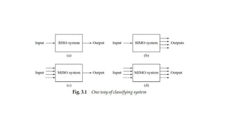
One way of classifying the systems is based on their input and output strength. For instance, when
the number of input to the system is one and the number of output is also one then such system is called
Single Input and Single Output or simply SISO system. Systems with other combinations such as Single
Input Multiple Output (SIMO), Multiple Input Single Output (MISO) and Multiple Input Multiple Output
(MIMO) also exist (Fig. 3.1).
The inputs and outputs can be in different form (For example, the input to an electrostatic actuator is voltage
whereas the output is displacement), however as far as energy is concerned, the input energy is equal to the
output energy provided that the system is an ideal one. In an ideal system, no losses are encountered.
46.
All systems arecategorized under four main basic or elemental systems, namely:
• Mechanical system • Fluid system • Electrical system • Thermal system
The inputs are the sources of energy, which are available. The noise is the unwanted energy that enters into the
system at any time. The noise energy is considered as the unwanted available input energy. So the total input energy
is the available input energy plus unwanted available input energy. The output energy is the difference between the
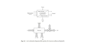
total input energy and the loss. Figure 3.2(a) illustrates a schematic diagram of a system, taking into account all
energy components. A system comprising all the inputs, outputs, noise and losses is rather called a ‘dynamic process’.
Y = f (U, N, X, P)
Where, U(t) and Y(t) are measurable input and output signals, N(t) is disturbance signal (noise), P(t) is slowly varying
process parameters and X(t) time dependent process state variables and are non-measurable parameters.
48.
The faults makea change in P(t) and in X(t) to produce P(t) + d P(t) and X(t) + d X(t), respectively. The inputs of a
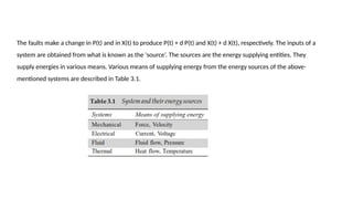
system are obtained from what is known as the ‘source’. The sources are the energy supplying entities. They
supply energies in various means. Various means of supplying energy from the energy sources of the above-
mentioned systems are described in Table 3.1.
49.
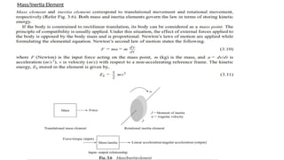
BASIC MODELING ELEMENTSIN MECHANICAL SYSTEM
Mechanical systems are the important basic building blocks of the MEMS systems. From the modeling schematic
and from the point of view of law of conservation of energy, distinguishably three basic modeling elements are
assigned for the mechanical systems. They are,
• Spring
• Damper
• Mass/Inertia
The fundamental comes from the fact that any kind of mechanical system has spring property, i.e. when force is
applied it elongates and the energy is stored within the system. It has also damping property, i.e. when force is
applied some portion of the force is lost. Finally it has mass or inertia property that determines how much
acceleration it would produce when exerted by the force .
For instance, the spring element stores potential energy, the damper represents the dissipating energy or loss
in the system and the inertia element stores kinetic energy.
50.
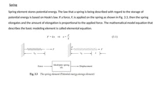
Spring
Spring element storespotential energy. The law that a spring is being described with regard to the storage of
potential energy is based on Hook’s law. If a force, F, is applied on the spring as shown in Fig. 3.3, then the spring
elongates and the amount of elongation is proportional to the applied force. The mathematical model equation that
describes the basic modeling element is called elemental equation.
51.
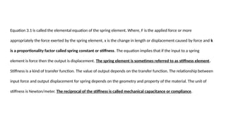
Equation 3.1 iscalled the elemental equation of the spring element. Where, F is the applied force or more
appropriately the force exerted by the spring element, x is the change in length or displacement caused by force and k
is a proportionality factor called spring constant or stiffness. The equation implies that if the input to a spring
element is force then the output is displacement. The spring element is sometimes referred to as stiffness element.
Stiffness is a kind of transfer function. The value of output depends on the transfer function. The relationship between
input force and output displacement for spring depends on the geometry and property of the material. The unit of
stiffness is Newton/meter. The reciprocal of the stiffness is called mechanical capacitance or compliance.
54.
Damper Element
Within thesystem loss is inevitable. The input energy minus the output energy is considered as loss energy, or simply
loss. In order to follow up the principle of conservation of energy a loss element should exist in order to describe the
system completely, i.e. the energy must be balanced. Indeed, the loss is reflected through the damper element.
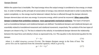
Damper element does not store any energy. It consumes energy, which cannot be recovered. Other name of the
damper is dashpot that symbolizes resistance, more appropriately mechanical resistance. Two types of dampers
such as translational dampers and rotational dampers are defined. Translational dampers and rotational dampers are
essentially related to translational movement and rotational movement, respectively. The symbols of the two types of
dampers are shown in Fig. 3.5. The loss is related to the velocity. In translational damper element the relationship
between the input force and velocity is linear as expressed in Eq. 3.6. This equation is the elemental equation for the
damper.
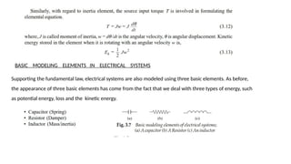
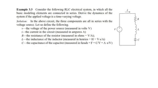
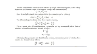
BASIC MODELING ELEMENTSIN ELECTRICAL SYSTEMS
Supporting the fundamental law, electrical systems are also modeled using three basic elements. As before,
the appearance of three basic elements has come from the fact that we deal with three types of energy, such
as potential energy, loss and the kinetic energy.