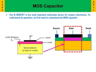
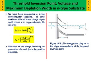
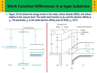
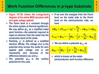
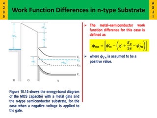
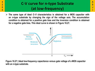
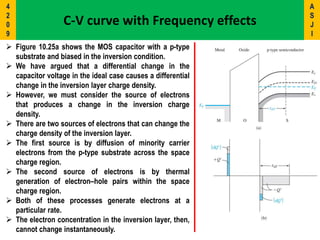
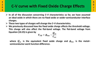
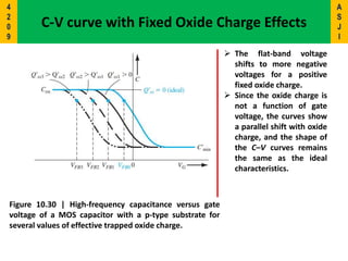
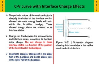
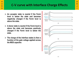
1) The document discusses the Metal-Oxide-Semiconductor (MOS) capacitor, which is important for understanding MOSFET operation.
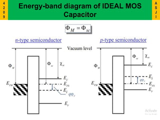
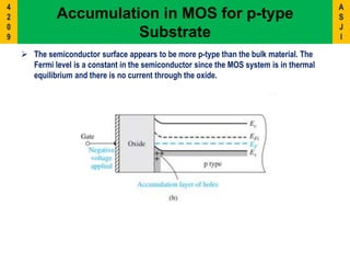
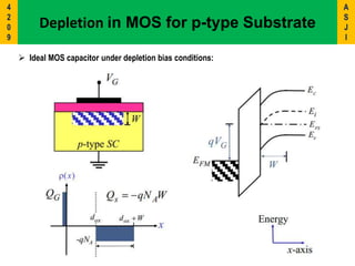
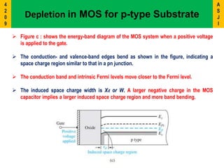
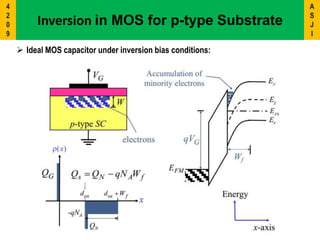
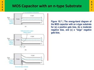
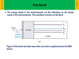
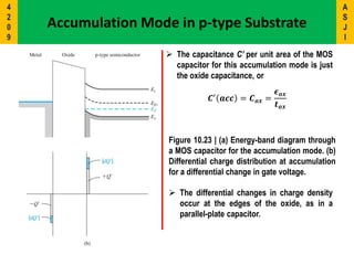
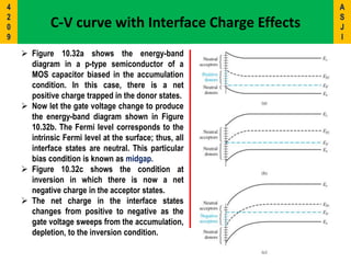
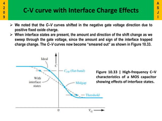
2) It describes the energy band diagrams and carrier accumulation, depletion, and inversion in MOS capacitors under different bias conditions for both p-type and n-type semiconductor substrates.
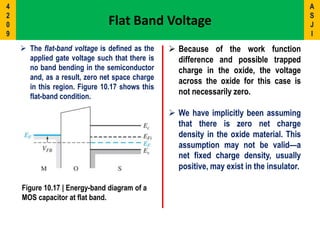
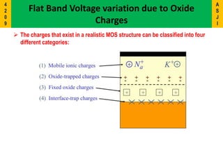
3) Key concepts covered include the flat-band voltage, threshold voltage, effects of oxide charges, and maximum depletion width.