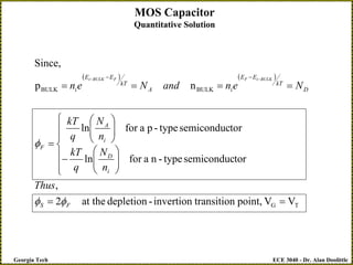
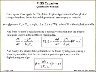
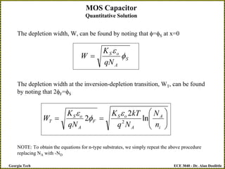
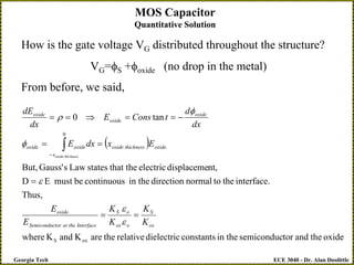
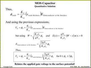
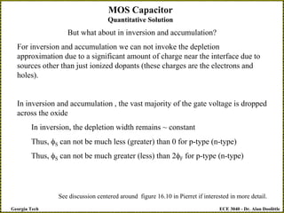
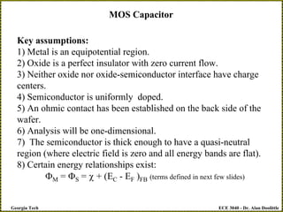
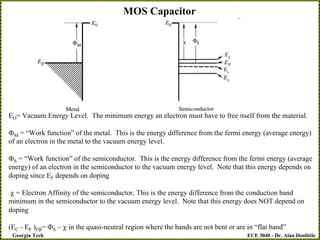
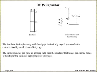
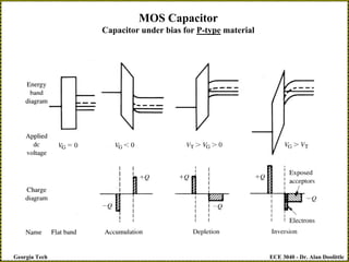
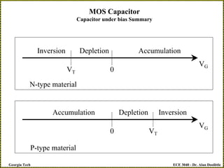
The document discusses a metal-oxide-semiconductor (MOS) capacitor. It describes the structure of an MOS capacitor, which consists of a metal gate electrode, insulating oxide layer, and doped semiconductor substrate. Depending on the applied gate voltage VG, the semiconductor near the interface can accumulate charge, deplete charge, or invert and accumulate the opposite charge type. The document provides quantitative equations to model the electrostatic potential and charge distribution within the semiconductor as a function of VG. It also relates VG to the potential drops across the oxide and semiconductor regions.
![ECE 3040 - Dr. Alan Doolittle
Georgia Tech
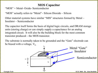
MOS Capacitor
Capacitor under bias
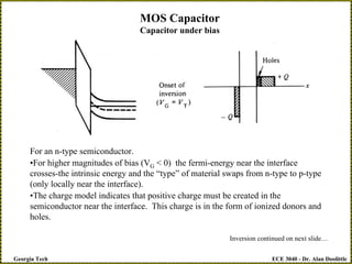
For an n-type semiconductor.
•When VG > 0 the metal fermi-energy is lowered (E=-qV), the insulator has
an electric field across it that terminates almost immediately in the near
perfectly conducting metal, but terminates over a finite distance in the
semiconductor of “finite resistivity”.
•The charge model indicates that negative charge must be created in the
semiconductor near the interface. This charge is in the form of electrons.
•Since n = niexp[(EF - Ei)/ kT], the electron concentration in the
semiconductor near interface increases.
•This is called accumulation](https://image.slidesharecdn.com/lecture23-moscapacitors-240308191013-2db78a13/85/Lecture-MOS-Capacitors-basic-for-MOSFET-pdf-pdf-9-320.jpg)
![ECE 3040 - Dr. Alan Doolittle
Georgia Tech
MOS Capacitor
Capacitor under bias
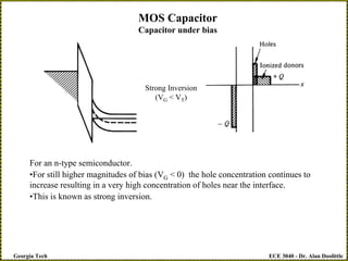
For an n-type semiconductor.
•When VG < 0 the metal fermi-energy is raised (E=-qV), the insulator has an
electric field across it that terminates almost immediately in the near perfectly
conducting metal, but terminates over a finite distance in the semiconductor of
“finite resistivity”.
•The charge model indicates that positive charge must be created in the
semiconductor near the interface. This charge is in the form of ionized donors.
•Since n = niexp[(EF - Ei)/ kT], the electron concentration in the semiconductor near
interface decreases.
•This is called depletion.](https://image.slidesharecdn.com/lecture23-moscapacitors-240308191013-2db78a13/85/Lecture-MOS-Capacitors-basic-for-MOSFET-pdf-pdf-10-320.jpg)
![ECE 3040 - Dr. Alan Doolittle
Georgia Tech
MOS Capacitor
Capacitor under bias
Inversion Continued…
•The hole concentration near the interface must equal the donor concentration. Thus,
pinterface = ND
pinterface = niexp[(Ei-INTERFACE -EF)/ kT] = niexp[(EF – Ei-BULK)/ kT]
•This is called inversion.
•The onset of inversion occurs for a voltage called the threshold voltage VT (not
thermal voltage)
•Detailed calculations taking into account the charge distribution as a function of
position in the semiconductor indicates that inversion occurs when,
Ei-INTERFACE - Ei-BULK = 2 (EF - Ei-BULK)](https://image.slidesharecdn.com/lecture23-moscapacitors-240308191013-2db78a13/85/Lecture-MOS-Capacitors-basic-for-MOSFET-pdf-pdf-12-320.jpg)
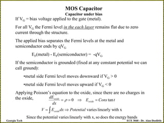
![ECE 3040 - Dr. Alan Doolittle
Georgia Tech
Let φ(x) = electrostatic potential inside
the semiconductor at a depth x (measured
from the oxide interface)
( ) ( )
[ ]
[ ]
[ ]
F
BULK
i
F
INTERFACE
i
BULK
i
S
i
BULK
i
E
E
q
with
along
potential
surface
E
E
q
x
E
E
q
x
−
=
≡
−
=
≡
−
=
−
−
−
−
1
,
1
and
potential
tic
electrosta
1
φ
φ
φ
MOS Capacitor
Quantitative Solution
P-type Example](https://image.slidesharecdn.com/lecture23-moscapacitors-240308191013-2db78a13/85/Lecture-MOS-Capacitors-basic-for-MOSFET-pdf-pdf-16-320.jpg)