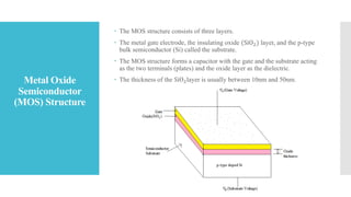
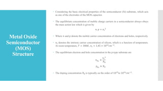
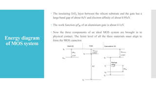
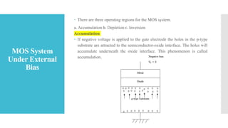
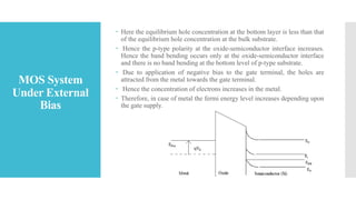
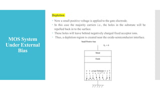
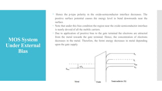
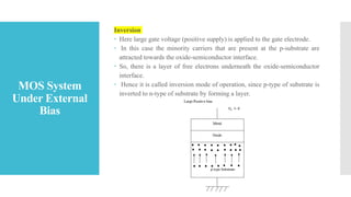
MOSSTRUCTURE
PREPARED BY
DEBASISH MOHANTA
DEPARTMENT OF ELECTRICAL ENGINEERING
GOVERNMENT COLLEGE OF ENGINEERING, KEONJHAR
MOS Transistor
 The MOS field effect transistor (MOSFET) is the fundamental building
block of MOS and CMOS digital integrated circuits.
 Compared to the bipolar junction transistor (BJT), the MOS transistor
occupies a relatively smaller Si area, and its fabrication used to involve
fewer processing steps.
 The technical advantages, together with the relative simplicity of MOSFET
operation, have helps make the MOS transistor the most widely switching
device in LSI and VLSI circuits.
Metal Oxide
Semiconductor
(MOS) Structure
 The MOS structure consists of three layers.
 The metal gate electrode, the insulating oxide (SiO2) layer, and the p-type
bulk semiconductor (Si) called the substrate.
 The MOS structure forms a capacitor with the gate and the substrate acting
as the two terminals (plates) and the oxide layer as the dielectric.
 The thickness of the SiO2layer is usually between 10nm and 50nm.
Metal Oxide
Semiconductor
(MOS)
Structure
 Considering the basic electrical properties of the semiconductor (Si) substrate, which acts
as one of the electrodes of the MOS capacitor.
 The equilibrium concentration of mobile charge carriers in a semiconductor always obeys
the mass action law which is given by
𝑛. 𝑝 = 𝑛𝑖
2
 Where 𝑛 and 𝑝 denote the mobile carrier concentration of electrons and holes, respectively.
 𝑛𝑖 denotes the intrinsic carrier concentration of silicon, which is a function of temperature.
At room temperature, 𝑇 = 300𝐾, 𝑛𝑖 = 1.45 × 10¹⁰
𝑐𝑚−3
.
 The equilibrium electron and hole concentration in the p-type substrate are
𝑛𝑝0
≅
𝑛𝑖
2
𝑁𝐴
𝑝𝑝0
≅ 𝑁𝐴
 The doping concentration 𝑁𝐴 is typically on the order of 1015
to 1016
𝑐𝑚−3
.
Energy band
diagram of p-
type substrate
 The band-gap between the conduction band and the valence band for silicon is approximately
1.1eV.
 The fermi potential, 𝜙𝐹 which is a function of temperature and doping, denotes the difference
between the intrinsic fermi level 𝐸𝑖 and fermi level 𝐸𝐹.
𝜙𝐹 =
𝐸𝐹 − 𝐸𝑖
𝑞
 For a p-type substrate, fermi potential can be approximated by
𝜙𝐹𝑝
=
𝐾𝑇
𝑞
ln
𝑛𝑖
𝑁𝐴
 where as for a n-type substrate, fermi potential is given by
𝜙𝐹𝑛
=
𝐾𝑇
𝑞
ln
𝑁𝐷
𝑛𝑖
 𝐾 denotes the Boltzmann constant and 𝑞 denotes the electronic charge and 𝑁𝐷 is the donor
concentration.
 The fermi potential is positive for n-type material and negative for p-type material.
Energy band
diagram of p-
type substrate
 The electron affinity, which is the energy required to remove an electron
from conduction band to vacuum level or free space is denoted by 𝑞𝜒.
 The work function, which is the energy required for an electron to move
from fermi level to free space is denoted by 𝑞𝜙𝑆.
𝑞𝜙𝑆 = 𝑞𝜒 + (𝐸𝐶 − 𝐸𝐹)
Energy diagram
of MOS system
 The insulating 𝑆𝑖𝑂2 layer between the silicon substrate and the gate has a
large band gap of about 8eV and electron affinity of about 0.95eV.
 The work function 𝑞𝐹𝑀 of an aluminium gate is about 4.1eV.
 Now the three components of an ideal MOS system are brought in to
physical contact. The fermi level of all the three materials must align to
form the MOS capacitor.
Energy diagram
of MOS system
 Because of the work function difference between the metal and
semiconductor, a voltage drop occurs across the MOS system.
 Part of this built-in voltage drop occurs across the insulating oxide layer.
 The rest of the voltage drop occurs at the silicon surface next to the silicon-
oxide interface forcing the energy bands of silicon to bend in this region.
Energy diagram
of MOS system
 Note that the equilibrium fermi levels of the semiconductor (Si) substrate
and the metal gate are at same potential.
 The bulk fermi level is not significantly affected by the band bending,
whereas the surface fermi level moves closer to the intrinsic fermi level.
 The fermi potential at the surface, also called surface potential 𝜙𝑆 is
smaller in magnitude than the bulk fermi potential 𝜙𝐹.
Example
 Consider the MOS structure that consists of a p type doped silicon
substrate, a silicon dioxide layer and a metal (aluminium) gate. The
equilibrium fermi potential of the doped silicon substrate is given by
𝑞𝜙𝐹𝑝
= 0.2𝑒𝑉. The electron affinity for Si is 4.15eV and the work function
of aluminium is 4.1eV. calculate the built-in potential difference across the
MOS system. Assume that the MOS system contains no other charges in
the oxide or on the silicon-oxide interface.
MOS Capacitor
 The metal oxide semiconductor structure is known as MOS capacitor.
 The expression for MOS capacitance can be written as
C = ϵox
A
tox
= ϵox
W × L
tox
 Where area of the MOS capacitor is A, tox is the oxide thickness and ϵox is
the dielectric constant of the oxide material.
MOS System
Under External
Bias
 There are three operating regions for the MOS system.
a. Accumulation b. Depletion c. Inversion
Accumulation
 If negative voltage is applied to the gate electrode the holes in the p-type
substrate are attracted to the semiconductor-oxide interface. The holes will
accumulate underneath the oxide interface. This phenomenon is called
accumulation.
MOS System
Under External
Bias
 Here the equilibrium hole concentration at the bottom layer is less than that
of the equilibrium hole concentration at the bulk substrate.
 Hence the p-type polarity at the oxide-semiconductor interface increases.
Hence the band bending occurs only at the oxide-semiconductor interface
and there is no band bending at the bottom level of p-type substrate.
 Due to application of negative bias to the gate terminal, the holes are
attracted from the metal towards the gate terminal.
 Hence the concentration of electrons increases in the metal.
 Therefore, in case of metal the fermi energy level increases depending upon
the gate supply.
MOS System
Under External
Bias
Depletion
 Now a small positive voltage is applied to the gate electrode.
 In this case the majority carriers i.e., the holes in the substrate will be
repelled back in to the surface.
 These holes will leave behind negatively charged fixed acceptor ions.
 Thus, a depletion region is created near the oxide-semiconductor interface.
MOS System
Under External
Bias
 Hence the p-type polarity in the oxide-semiconductor interface decreases. The
positive surface potential causes the energy level to bend downwards near the
surface.
 Note that under this bias condition the region near the oxide-semiconductor interface
is nearly devoid of all the mobile carriers.
 Due to application of positive bias to the gate terminal the electrons are attracted
from the metal towards the gate terminal. Hence, the concentration of electrons
decreases in the metal. Therefore, the fermi energy decreases in metal depending
upon the gate supply.
MOS System
Under External
Bias
Inversion
 Here large gate voltage (positive supply) is applied to the gate electrode.
 In this case the minority carriers that are present at the p-substrate are
attracted towards the oxide-semiconductor interface.
 So, there is a layer of free electrons underneath the oxide-semiconductor
interface.
 Hence it is called inversion mode of operation, since p-type of substrate is
inverted to n-type of substrate by forming a layer.
MOS System
Under External
Bias
 Due to the application of more gate voltage, there is an occurrence of more
band bending.
 Hence the intrinsic fermi energy level crosses the EFP.
 Here p-type substrate is inverted to n-type substrate which is clearly visible
from the band diagram underneath the interface.
 The minimum voltage required to form a channel in between source and
drain is called threshold voltage.

MOS Structure.pptx

  • 1.
    MOSSTRUCTURE PREPARED BY DEBASISH MOHANTA DEPARTMENTOF ELECTRICAL ENGINEERING GOVERNMENT COLLEGE OF ENGINEERING, KEONJHAR
  • 2.
    MOS Transistor  TheMOS field effect transistor (MOSFET) is the fundamental building block of MOS and CMOS digital integrated circuits.  Compared to the bipolar junction transistor (BJT), the MOS transistor occupies a relatively smaller Si area, and its fabrication used to involve fewer processing steps.  The technical advantages, together with the relative simplicity of MOSFET operation, have helps make the MOS transistor the most widely switching device in LSI and VLSI circuits.
  • 3.
    Metal Oxide Semiconductor (MOS) Structure The MOS structure consists of three layers.  The metal gate electrode, the insulating oxide (SiO2) layer, and the p-type bulk semiconductor (Si) called the substrate.  The MOS structure forms a capacitor with the gate and the substrate acting as the two terminals (plates) and the oxide layer as the dielectric.  The thickness of the SiO2layer is usually between 10nm and 50nm.
  • 4.
    Metal Oxide Semiconductor (MOS) Structure  Consideringthe basic electrical properties of the semiconductor (Si) substrate, which acts as one of the electrodes of the MOS capacitor.  The equilibrium concentration of mobile charge carriers in a semiconductor always obeys the mass action law which is given by 𝑛. 𝑝 = 𝑛𝑖 2  Where 𝑛 and 𝑝 denote the mobile carrier concentration of electrons and holes, respectively.  𝑛𝑖 denotes the intrinsic carrier concentration of silicon, which is a function of temperature. At room temperature, 𝑇 = 300𝐾, 𝑛𝑖 = 1.45 × 10¹⁰ 𝑐𝑚−3 .  The equilibrium electron and hole concentration in the p-type substrate are 𝑛𝑝0 ≅ 𝑛𝑖 2 𝑁𝐴 𝑝𝑝0 ≅ 𝑁𝐴  The doping concentration 𝑁𝐴 is typically on the order of 1015 to 1016 𝑐𝑚−3 .
  • 5.
    Energy band diagram ofp- type substrate  The band-gap between the conduction band and the valence band for silicon is approximately 1.1eV.  The fermi potential, 𝜙𝐹 which is a function of temperature and doping, denotes the difference between the intrinsic fermi level 𝐸𝑖 and fermi level 𝐸𝐹. 𝜙𝐹 = 𝐸𝐹 − 𝐸𝑖 𝑞  For a p-type substrate, fermi potential can be approximated by 𝜙𝐹𝑝 = 𝐾𝑇 𝑞 ln 𝑛𝑖 𝑁𝐴  where as for a n-type substrate, fermi potential is given by 𝜙𝐹𝑛 = 𝐾𝑇 𝑞 ln 𝑁𝐷 𝑛𝑖  𝐾 denotes the Boltzmann constant and 𝑞 denotes the electronic charge and 𝑁𝐷 is the donor concentration.  The fermi potential is positive for n-type material and negative for p-type material.
  • 6.
    Energy band diagram ofp- type substrate  The electron affinity, which is the energy required to remove an electron from conduction band to vacuum level or free space is denoted by 𝑞𝜒.  The work function, which is the energy required for an electron to move from fermi level to free space is denoted by 𝑞𝜙𝑆. 𝑞𝜙𝑆 = 𝑞𝜒 + (𝐸𝐶 − 𝐸𝐹)
  • 7.
    Energy diagram of MOSsystem  The insulating 𝑆𝑖𝑂2 layer between the silicon substrate and the gate has a large band gap of about 8eV and electron affinity of about 0.95eV.  The work function 𝑞𝐹𝑀 of an aluminium gate is about 4.1eV.  Now the three components of an ideal MOS system are brought in to physical contact. The fermi level of all the three materials must align to form the MOS capacitor.
  • 8.
    Energy diagram of MOSsystem  Because of the work function difference between the metal and semiconductor, a voltage drop occurs across the MOS system.  Part of this built-in voltage drop occurs across the insulating oxide layer.  The rest of the voltage drop occurs at the silicon surface next to the silicon- oxide interface forcing the energy bands of silicon to bend in this region.
  • 9.
    Energy diagram of MOSsystem  Note that the equilibrium fermi levels of the semiconductor (Si) substrate and the metal gate are at same potential.  The bulk fermi level is not significantly affected by the band bending, whereas the surface fermi level moves closer to the intrinsic fermi level.  The fermi potential at the surface, also called surface potential 𝜙𝑆 is smaller in magnitude than the bulk fermi potential 𝜙𝐹. Example  Consider the MOS structure that consists of a p type doped silicon substrate, a silicon dioxide layer and a metal (aluminium) gate. The equilibrium fermi potential of the doped silicon substrate is given by 𝑞𝜙𝐹𝑝 = 0.2𝑒𝑉. The electron affinity for Si is 4.15eV and the work function of aluminium is 4.1eV. calculate the built-in potential difference across the MOS system. Assume that the MOS system contains no other charges in the oxide or on the silicon-oxide interface.
  • 10.
    MOS Capacitor  Themetal oxide semiconductor structure is known as MOS capacitor.  The expression for MOS capacitance can be written as C = ϵox A tox = ϵox W × L tox  Where area of the MOS capacitor is A, tox is the oxide thickness and ϵox is the dielectric constant of the oxide material.
  • 11.
    MOS System Under External Bias There are three operating regions for the MOS system. a. Accumulation b. Depletion c. Inversion Accumulation  If negative voltage is applied to the gate electrode the holes in the p-type substrate are attracted to the semiconductor-oxide interface. The holes will accumulate underneath the oxide interface. This phenomenon is called accumulation.
  • 12.
    MOS System Under External Bias Here the equilibrium hole concentration at the bottom layer is less than that of the equilibrium hole concentration at the bulk substrate.  Hence the p-type polarity at the oxide-semiconductor interface increases. Hence the band bending occurs only at the oxide-semiconductor interface and there is no band bending at the bottom level of p-type substrate.  Due to application of negative bias to the gate terminal, the holes are attracted from the metal towards the gate terminal.  Hence the concentration of electrons increases in the metal.  Therefore, in case of metal the fermi energy level increases depending upon the gate supply.
  • 13.
    MOS System Under External Bias Depletion Now a small positive voltage is applied to the gate electrode.  In this case the majority carriers i.e., the holes in the substrate will be repelled back in to the surface.  These holes will leave behind negatively charged fixed acceptor ions.  Thus, a depletion region is created near the oxide-semiconductor interface.
  • 14.
    MOS System Under External Bias Hence the p-type polarity in the oxide-semiconductor interface decreases. The positive surface potential causes the energy level to bend downwards near the surface.  Note that under this bias condition the region near the oxide-semiconductor interface is nearly devoid of all the mobile carriers.  Due to application of positive bias to the gate terminal the electrons are attracted from the metal towards the gate terminal. Hence, the concentration of electrons decreases in the metal. Therefore, the fermi energy decreases in metal depending upon the gate supply.
  • 15.
    MOS System Under External Bias Inversion Here large gate voltage (positive supply) is applied to the gate electrode.  In this case the minority carriers that are present at the p-substrate are attracted towards the oxide-semiconductor interface.  So, there is a layer of free electrons underneath the oxide-semiconductor interface.  Hence it is called inversion mode of operation, since p-type of substrate is inverted to n-type of substrate by forming a layer.
  • 16.
    MOS System Under External Bias Due to the application of more gate voltage, there is an occurrence of more band bending.  Hence the intrinsic fermi energy level crosses the EFP.  Here p-type substrate is inverted to n-type substrate which is clearly visible from the band diagram underneath the interface.  The minimum voltage required to form a channel in between source and drain is called threshold voltage.