Downloaded 123 times

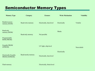
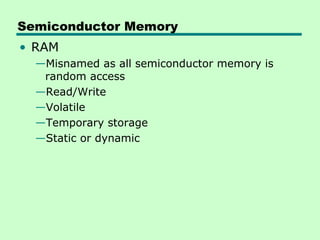
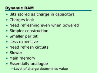
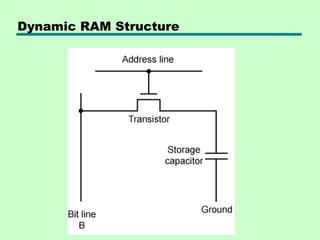
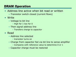
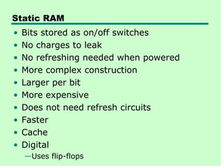
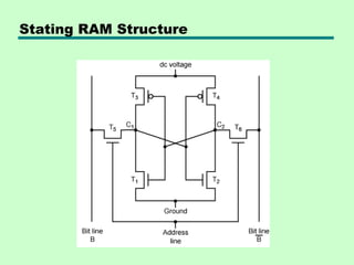
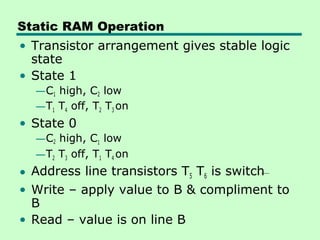
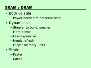
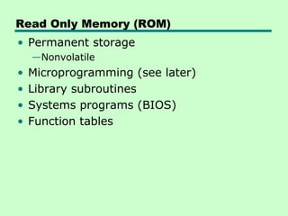

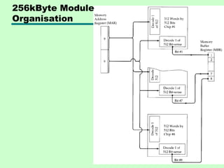
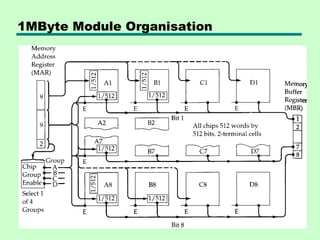

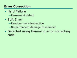
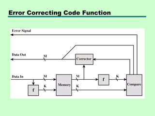
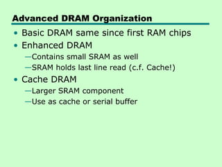
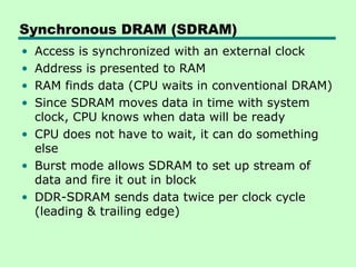
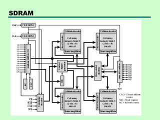
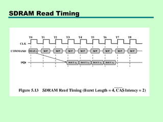
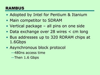
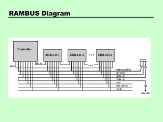
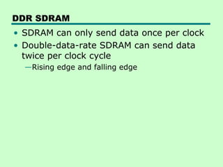
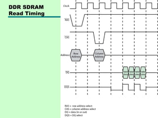
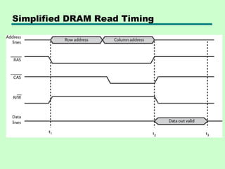
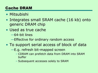


1. The document discusses different types of semiconductor memory including RAM, ROM, PROM, EPROM, EEPROM, and flash memory. 2. It describes the operation and structure of both dynamic RAM (DRAM) and static RAM (SRAM). DRAM uses capacitors to store bits and requires refreshing, while SRAM uses flip-flops and does not require refreshing. 3. The document also covers various RAM technologies including synchronous DRAM (SDRAM), double data rate SDRAM (DDR SDRAM), Rambus DRAM (RDRAM), error correction codes, and cache DRAM.


![Getting Started with Apache Spark: Big Data Made Simple [Free Meetup]](https://cdn.slidesharecdn.com/ss_thumbnails/apachesparkgettingstarted-260203175547-8361bcc3-thumbnail.jpg?width=640&height=640&fit=bounds)


