Introduction
• Memory isone of the most important functional units of a computer.
• Used to store both instructions and data.
• Stores as bits (0’s and 1’s), usually organized in terms of bytes.
• How are the data stored in memory accessed?
• Every memory location has a unique address.
• A memory is said to be byte addressable if every byte of data has a unique
address.
• Some memory systems are word addressable also (every addressed loca8ons
consists of multiple bytes, say, 32 bits or 4 bytes).
3.
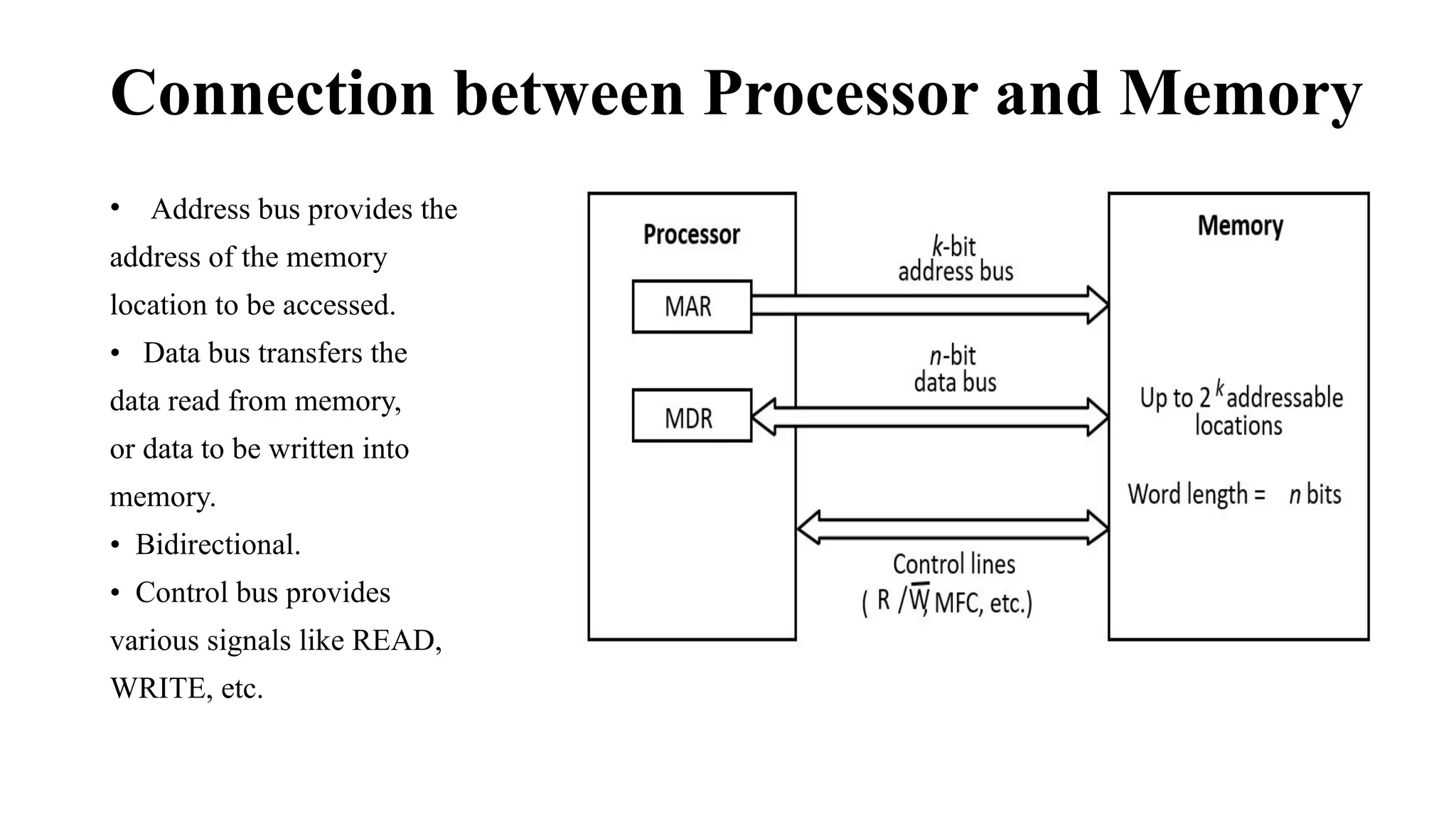
Connection between Processorand Memory
• Address bus provides the
address of the memory
location to be accessed.
• Data bus transfers the
data read from memory,
or data to be written into
memory.
• Bidirectional.
• Control bus provides
various signals like READ,
WRITE, etc.
4.
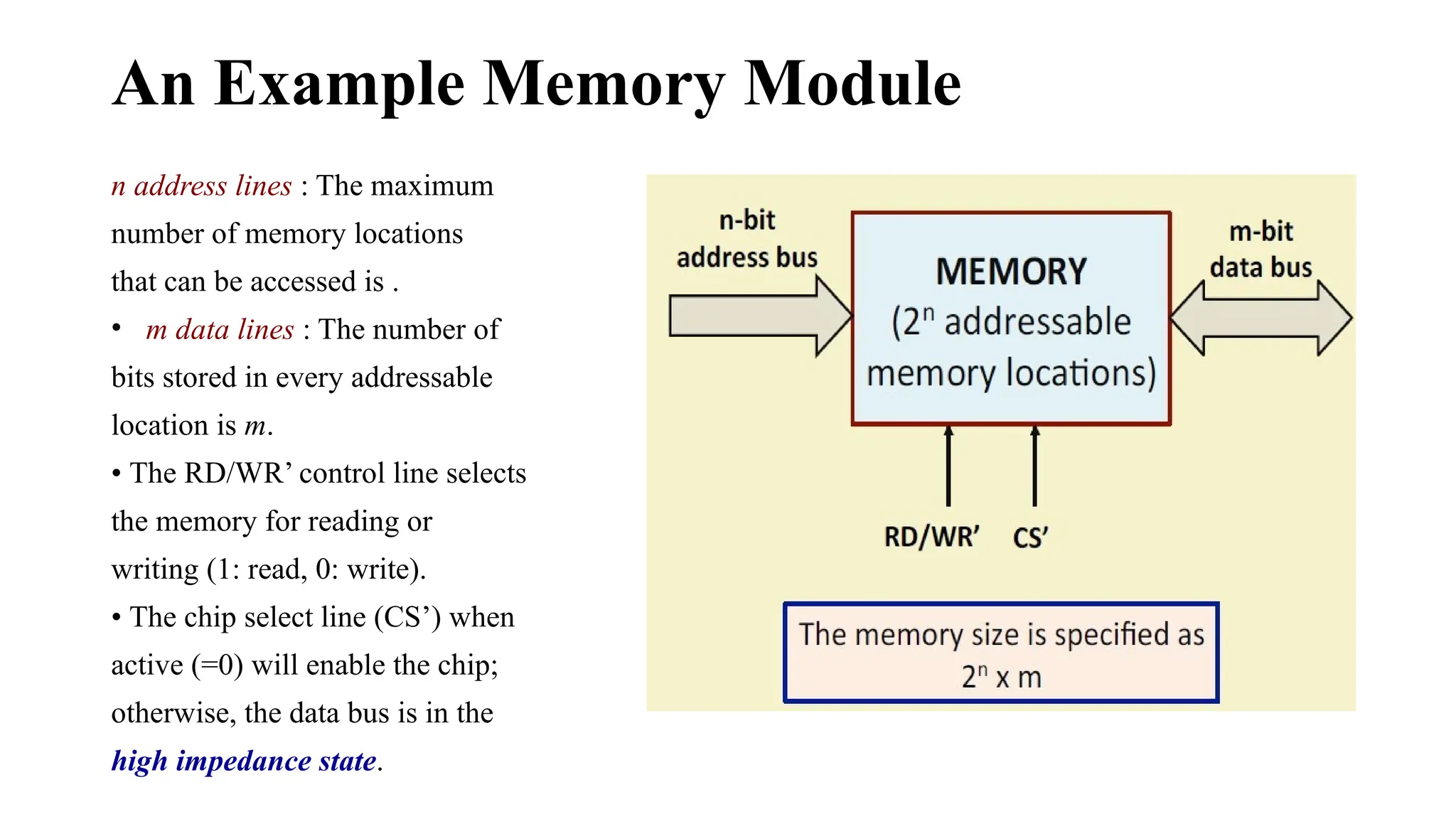
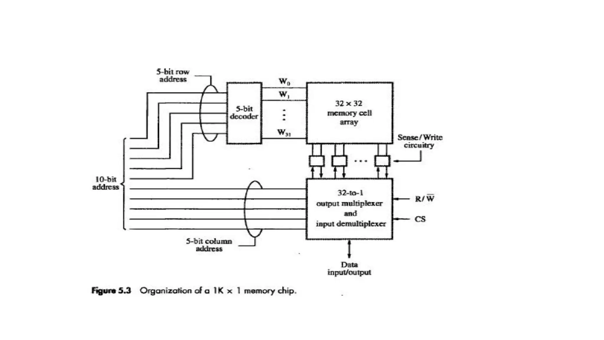
An Example MemoryModule
n address lines : The maximum
number of memory locations
that can be accessed is .
• m data lines : The number of
bits stored in every addressable
location is m.
• The RD/WR’ control line selects
the memory for reading or
writing (1: read, 0: write).
• The chip select line (CS’) when
active (=0) will enable the chip;
otherwise, the data bus is in the
high impedance state.
5.
Classification of MemorySystems
a) Volatile versus Non-volatile:
• A volatile memory system is one where the stored data is lost when the
power is switched off.
Examples: CMOS static memory, CMOS dynamic memory.
Dynamic memory in addition requires periodic refreshing.
• A non-volatile memory system is one where the stored data is retained
even when the power is switched off.
Examples: Read-only memory, Magnetic disk, CDROM/DVD, Flash memory,Resistive memory.
6.
b) Random-access versusDirect/Sequential access:
– A memory is said to be random-access when the read/write 8me is
independent of the memory location being accessed.
• Examples: CMOS memory (RAM and ROM).
– A memory is said to be sequential access when the stored data can
only be accessed sequentially in a particular order.
• Examples: Magnetic tape.
– A memory is said to be direct or semi-random access when part of the
access is sequential and part is random.
• Example: Magnetic disk.
• We can directly go to a track after which access will be sequential.
7.
c) Read-only versusRandom-access:
– Read-only Memory (ROM) is one where data once stored in permanent
or semi-permanent.
• Data written (programmed) during manufacture or in the laboratory.
• Examples: ROM, PROM, EPROM, EEPROM.
– Random Access Memory (RAM) is one where data access time is the
same independent of the location (address).
• Used in main / cache memory systems.
• Example: Static RAM (SRAM) à data once written are retained as long as
power is on.
• Example: Dynamic RAM (DRAM) à requires periodic refreshing even when
power is on (data stored as charge on tiny capacitors).
8.
• Some importantquestions?
– How to make the memory system work faster?
– How to increase the data transfer rate between CPU and memory?
– How to address the ever increasing storage needs of applications?
• Some possible solutions:
– Cache Memory: to increase the effective speed of the memory system.
– Virtual Memory: to increase the effective size of the memory system.
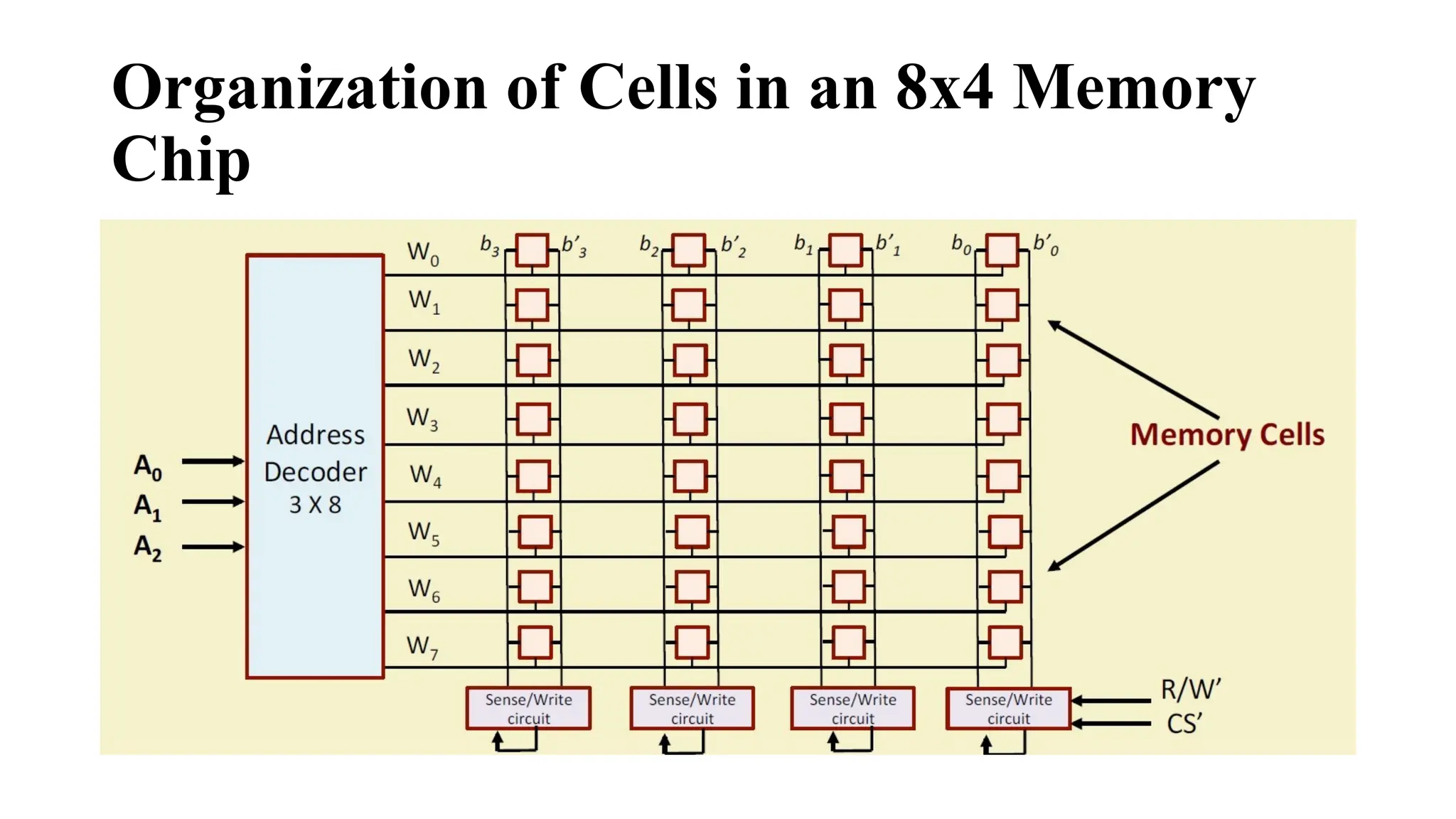
Organization of Cellsin an 8x4 Memory Chip (cont..)
• A 32-bit memory chip organized as 8 x 4 is shown.
• Every row of the cell array constitutes a memory word.
• A 3 x 8 decoder is required to access any one of the 8 rows.
• The rows of the cells are connected to the word lines.
• Individual cells are connected to two bit lines.
– Bit b and its complement b’.
– Required for reading and writing.
• Cells in each column are connected to a sense/write circuit by the two bit
lines.
• Other than address and data lines, there are two control lines: R/W’ and
CS’ (Chip Select).
– CS is required to select one single chip in a multi-chip memory system.
12.
Static Random AccessMemory (SRAM)
• SRAM consists of circuits which can store the data as long as power is applied.
• It is a type of semiconductor memory that uses bistable latching circuitry (flip-flop) to store each
bit.
• SRAM memory arrays can be arranged in rows and columns of memory cells.
– Called word line and bit line.
• SRAM can be built using 4 or 6 MOS transistors.
– Modern SRAM chips in the market uses 6-transistor implementations for CMOS compatibility.
– Widely used in small-scale systems like microcontrollers and embedded systems.
– Also used to implement cache memories in computer systems.
13.
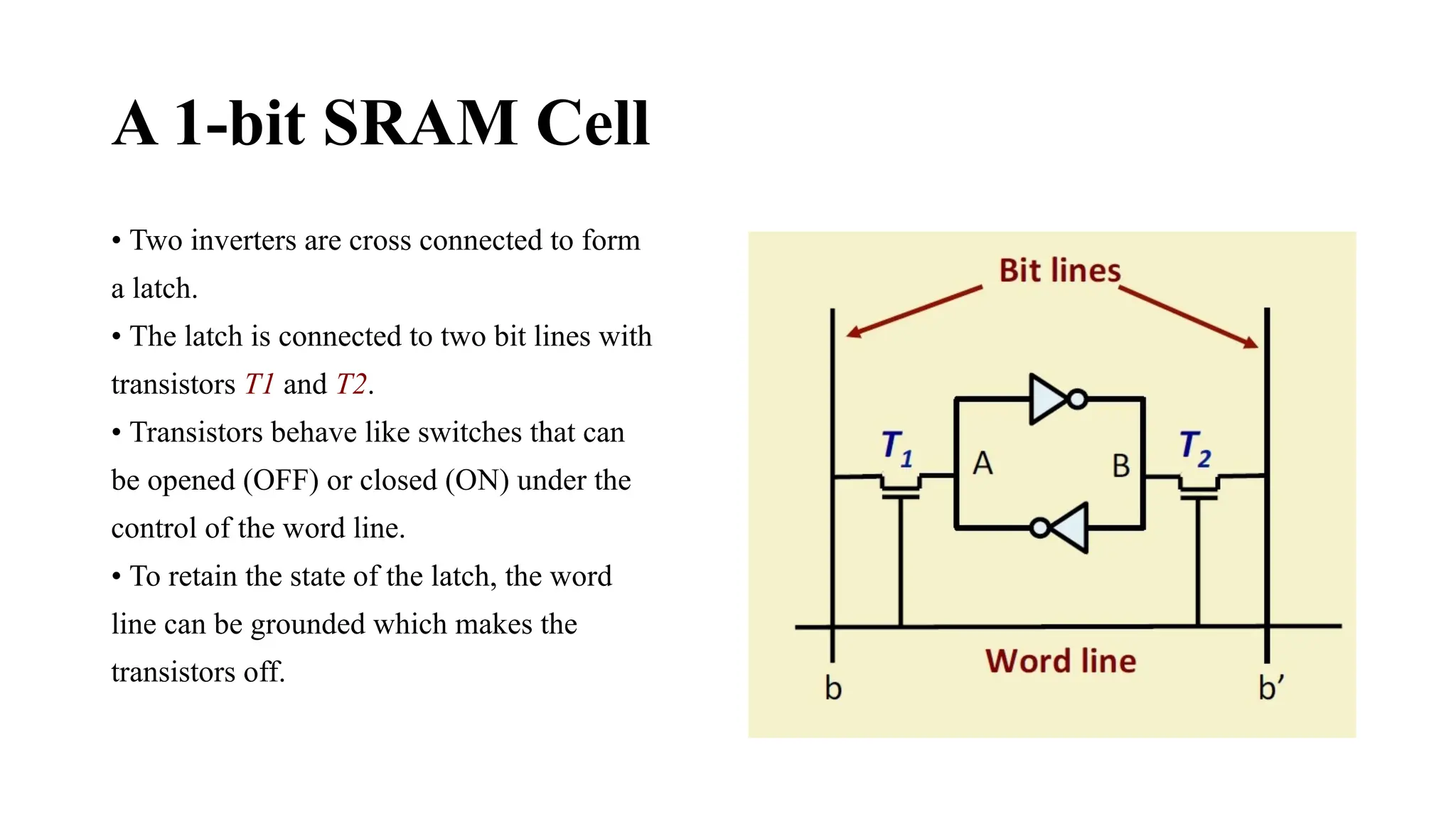
A 1-bit SRAMCell
• Two inverters are cross connected to form
a latch.
• The latch is connected to two bit lines with
transistors T1 and T2.
• Transistors behave like switches that can
be opened (OFF) or closed (ON) under the
control of the word line.
• To retain the state of the latch, the word
line can be grounded which makes the
transistors off.
14.
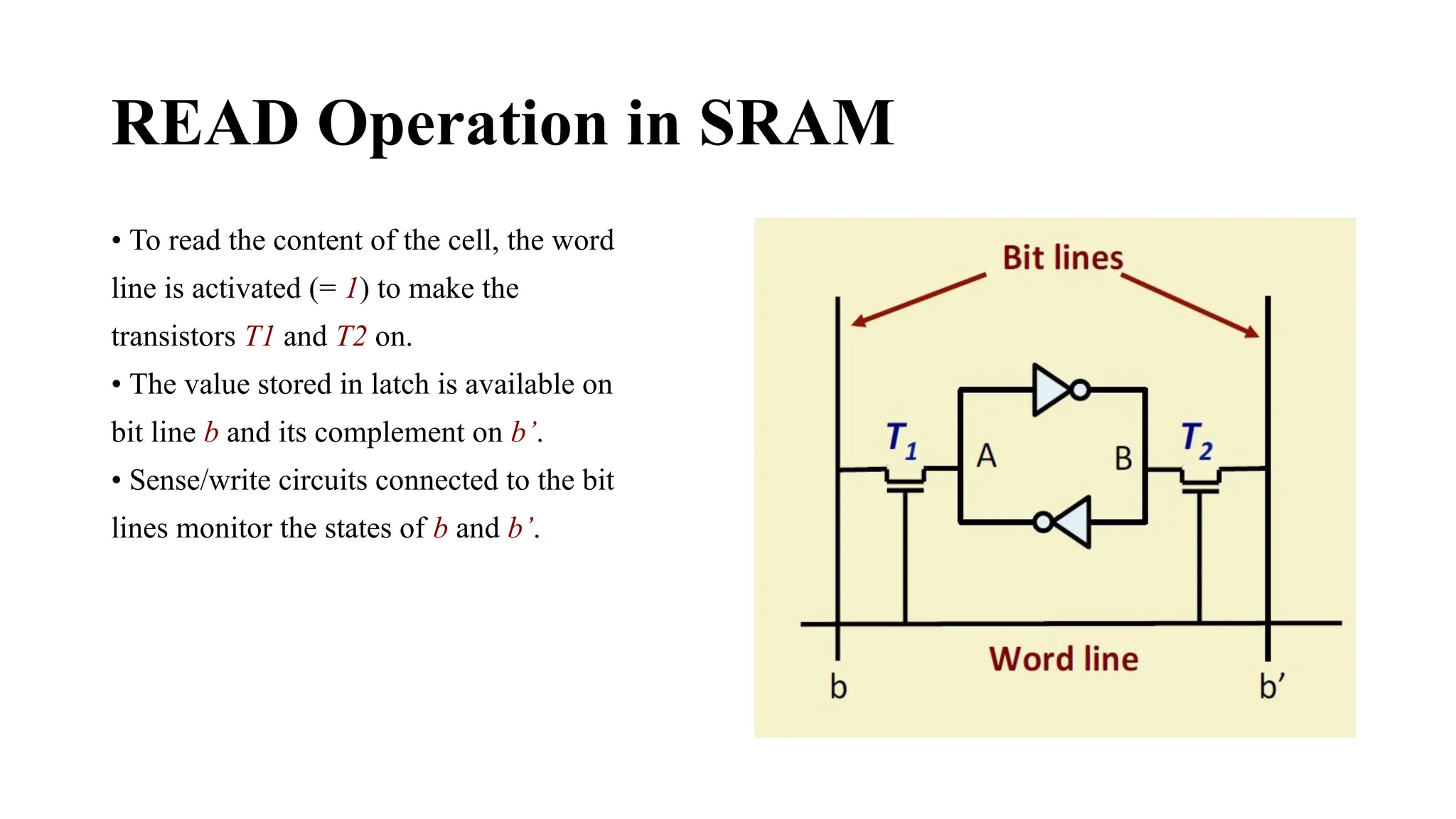
READ Operation inSRAM
• To read the content of the cell, the word
line is activated (= 1) to make the
transistors T1 and T2 on.
• The value stored in latch is available on
bit line b and its complement on b’.
• Sense/write circuits connected to the bit
lines monitor the states of b and b’.
15.
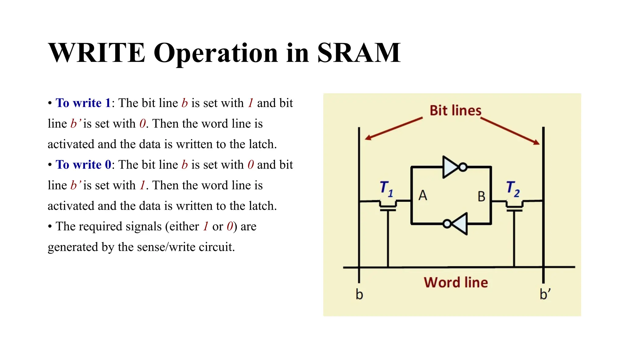
WRITE Operation inSRAM
• To write 1: The bit line b is set with 1 and bit
line b’is set with 0. Then the word line is
activated and the data is written to the latch.
• To write 0: The bit line b is set with 0 and bit
line b’is set with 1. Then the word line is
activated and the data is written to the latch.
• The required signals (either 1 or 0) are
generated by the sense/write circuit.
16.
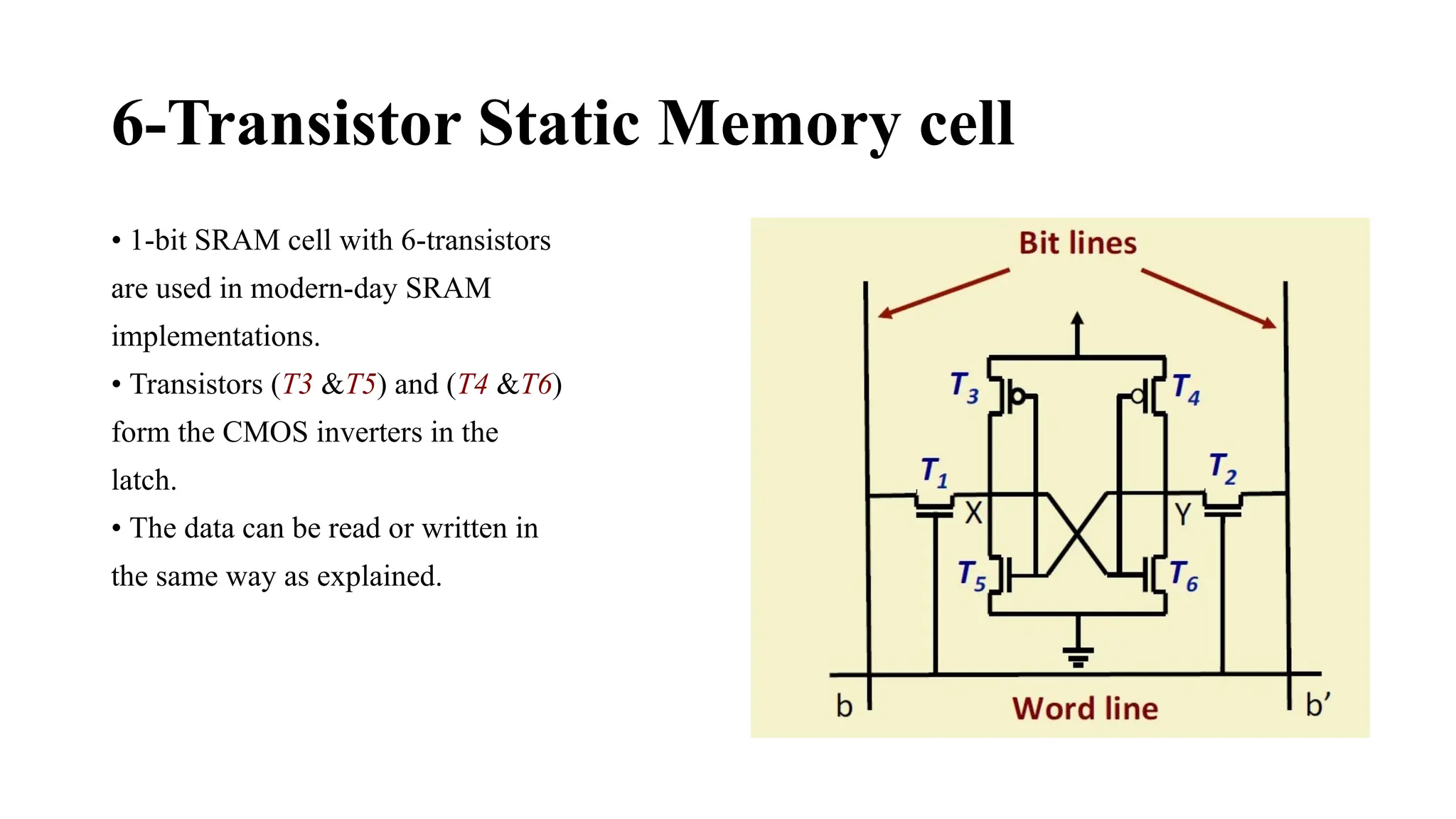
6-Transistor Static Memorycell
• 1-bit SRAM cell with 6-transistors
are used in modern-day SRAM
implementations.
• Transistors (T3 &T5) and (T4 &T6)
form the CMOS inverters in the
latch.
• The data can be read or written in
the same way as explained.
17.
Features of SRAM
•Moderate / High power consumption.
– Current flows in the cells only when the cell is accessed.
– Because of latch operation, power consumption is higher than DRAM.
• Simplicity – refresh circuitry is not needed.
– Volatile :: continuous power supply is required.
• Fast operation.
– Access time is very fast; fast memories (cache) are built using SRAM.
• High cost.
– 6 transistors per cell.
• Limited capacity.
– Not economical to manufacture high-capacity SRAM chips.
18.
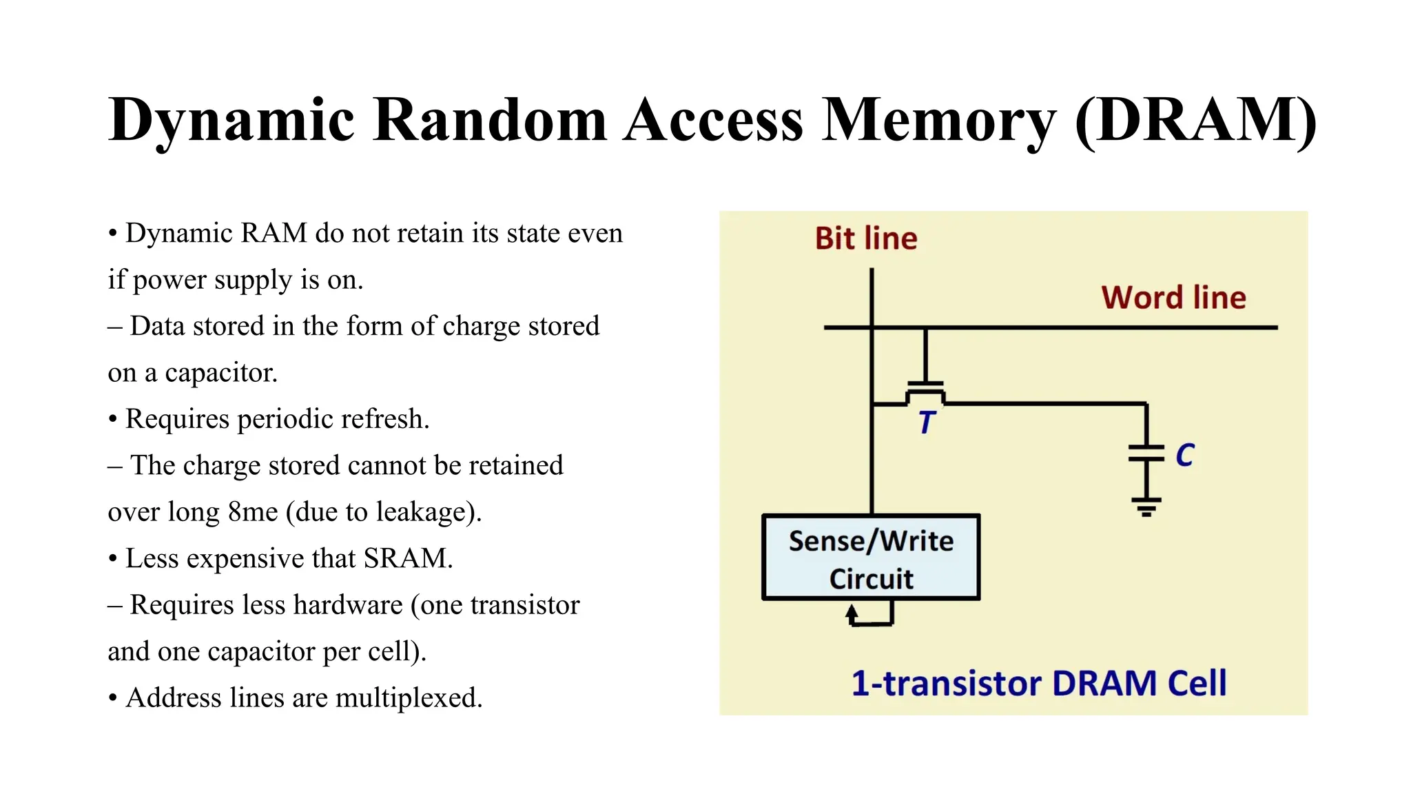
Dynamic Random AccessMemory (DRAM)
• Dynamic RAM do not retain its state even
if power supply is on.
– Data stored in the form of charge stored
on a capacitor.
• Requires periodic refresh.
– The charge stored cannot be retained
over long 8me (due to leakage).
• Less expensive that SRAM.
– Requires less hardware (one transistor
and one capacitor per cell).
• Address lines are multiplexed.
19.
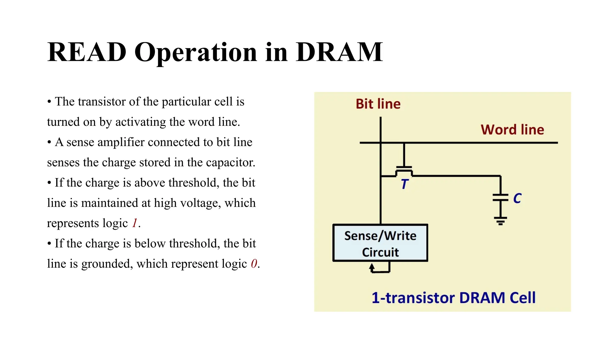
READ Operation inDRAM
• The transistor of the particular cell is
turned on by activating the word line.
• A sense amplifier connected to bit line
senses the charge stored in the capacitor.
• If the charge is above threshold, the bit
line is maintained at high voltage, which
represents logic 1.
• If the charge is below threshold, the bit
line is grounded, which represent logic 0.
20.
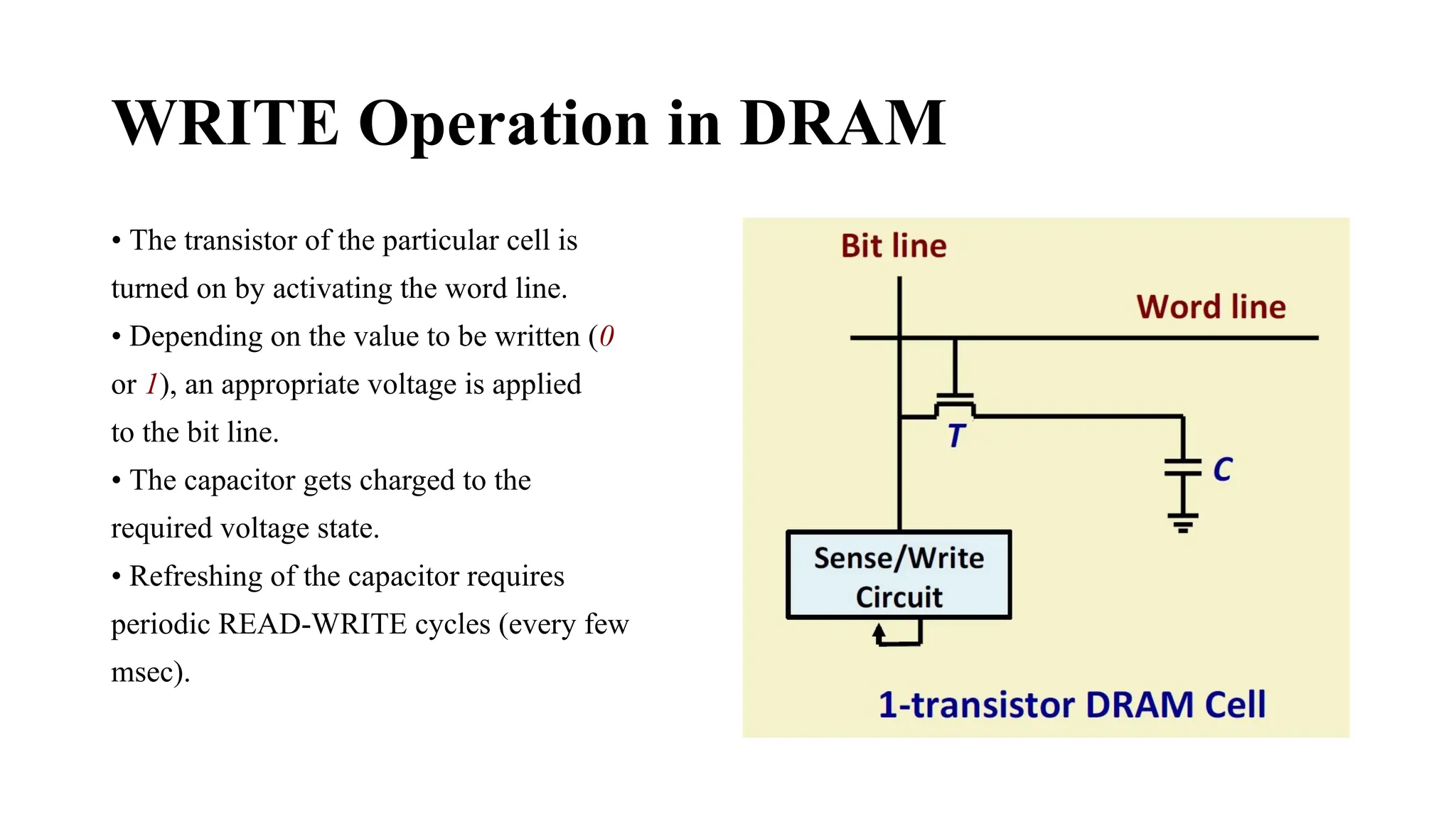
WRITE Operation inDRAM
• The transistor of the particular cell is
turned on by activating the word line.
• Depending on the value to be written (0
or 1), an appropriate voltage is applied
to the bit line.
• The capacitor gets charged to the
required voltage state.
• Refreshing of the capacitor requires
periodic READ-WRITE cycles (every few
msec).
21.
Read-Only Memories
Read-OnlyMemory:
Data are written into a ROM when it is manufactured.
Programmable Read-Only Memory (PROM):
Allow the data to be loaded by a user.
Process of inserting the data is irreversible.
Storing information specific to a user in a ROM is expensive.
Providing programming capability to a user may be better.
Erasable Programmable Read-Only Memory (EPROM):
Stored data to be erased and new data to be loaded.
Flexibility, useful during the development phase of digital systems.
Erasable, reprogrammable ROM.
Erasure requires exposing the ROM to UV light.
22.
Read-Only Memories (Contd.,)
Electrically Erasable Programmable Read-Only Memory (EEPROM):
To erase the contents of EPROMs, they have to be exposed to ultraviolet light.
Physically removed from the circuit.
EEPROMs the contents can be stored and erased electrically.
Flash memory:
Has similar approach to EEPROM.
Read the contents of a single cell, but write the contents of an entire block of cells.
Flash devices have greater density.
▪ Higher capacity and low storage cost per bit.
Power consumption of flash memory is very low, making it attractive for use in equipment that is
battery-driven.
Single flash chips are not sufficiently large, so
larger memory modules are implemented using
flash cards and flash drives.
23.
Speed, Size, andCost
A big challenge in the design of a computer system is to provide a sufficiently large memory,
with a reasonable speed at an affordable cost.
Static RAM:
Very fast, but expensive, because a basic SRAM cell has a complex circuit making it
impossible to pack a large number of cells onto a single chip.
Dynamic RAM:
Simpler basic cell circuit, hence are much less expensive, but significantly slower than
SRAMs.
Magnetic disks:
Storage provided by DRAMs is higher than SRAMs, but is still less than what is necessary.
Secondary storage such as magnetic disks provide a large amount
of storage, but is much slower than DRAMs.
24.
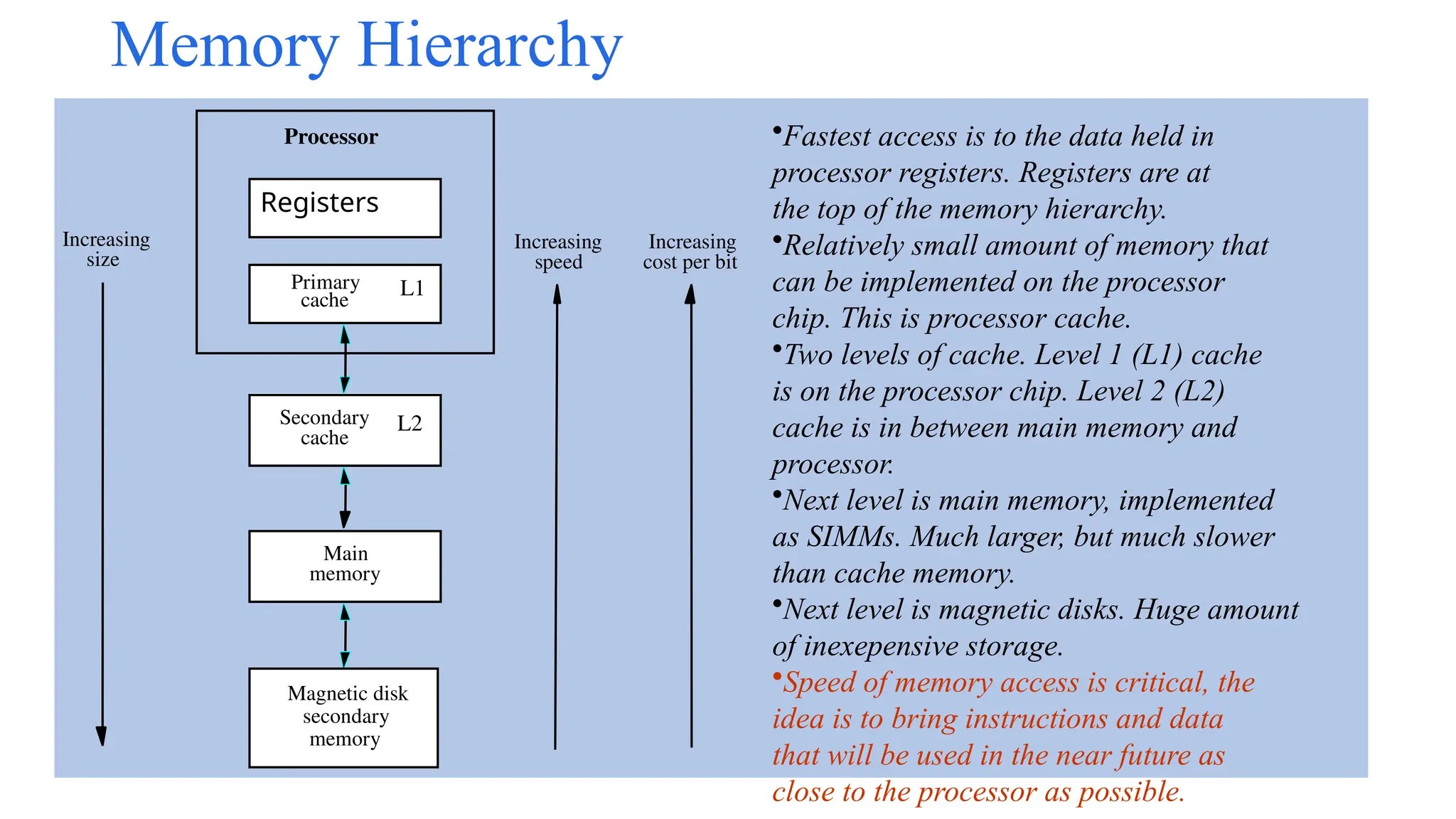
Memory Hierarchy
Processor
Primary
cache
Main
memory
Increasing
size
Increasing
speed
Magnetic disk
secondary
memory
Increasing
costper bit
Registers
L1
Secondary
cache
L2
•Fastest access is to the data held in
processor registers. Registers are at
the top of the memory hierarchy.
•Relatively small amount of memory that
can be implemented on the processor
chip. This is processor cache.
•Two levels of cache. Level 1 (L1) cache
is on the processor chip. Level 2 (L2)
cache is in between main memory and
processor.
•Next level is main memory, implemented
as SIMMs. Much larger, but much slower
than cache memory.
•Next level is magnetic disks. Huge amount
of inexepensive storage.
•Speed of memory access is critical, the
idea is to bring instructions and data
that will be used in the near future as
close to the processor as possible.