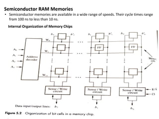
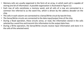
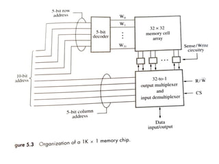
Computer
Organization and
Architecture
MODULE 4
SUBJECT CODE: 18EC35
SAVITA M
ASSISTANT PROFESSOR
DEPT. OF ECE
JIT
THE MEMORY SYSTEM
Some Basic Concepts
• Memory Access Time: the time that elapses between the initiation of
an operation and the completion of that operation.
• For example, the time between the Read and the MFC signals.
• Memory Cycle Time: which is the minimum time delay required
between the initiation of two successive memory operations.
• For example, the time between two successive Read operations.
• Random Access Memory (RAM): A memory unit is called
random-access memory (RAM) if any location can be accessed for a
Read or Write operation in some fixed amount of time that is
independent of the location's address.
• The basic technology for implementing the memory uses
semiconductor integrated circuits.
Semiconductor RAM Memories
• Semiconductor memories are available in a wide range of speeds. Their cycle times range
from 100 ns to less than 10 ns.
Internal Organization of Memory Chips
• Memory cells are usually organized in the form of an array, in which each cell is capable of
storing one bit of information. A possible organization is illustrated in Figure 5.2.
• Each row of cells constitutes a memory word, and all cells of a row are connected to a
common line referred to as the word line, which is driven by the address decoder on the
chip.
• The cells in each column are connected to a Sense/Write circuit by two bit lines.
• The Sense/Write circuits are connected to the data input/output lines of the chip.
• During a Read operation, these circuits sense, or read, the information stored in the cells
selected by a word line and transmit this information to the output data lines.
• During a Write operation, the Sense/Write circuits receive input information and store it in
the cells of the selected word.
• The required 10-bit address is divided into two groups of 5
bits each to form the row and column addresses for the
cell array.
• A row address selects a row of 32 cells, all of which are
accessed in parallel.
• However, according to the column address, only one of
these cells is connected to the external data line by the
output multiplexer and input demultiplexer.
• Commercially available memory chips contain a much
larger number of memory cells than the examples shown
in Figures 5.2 and 5.3.
• For example, a 4M-bit chip may have a 512K x 8
organization, in which case 19 address and 8 data
input/output pins are needed.
Static Memories
• Memories that consist of circuits capable of retaining their state
as long as power is applied are known as static memories.
• Figure 5.4 illustrates how a static RAM (SRAM) cell may be
implemented.
• Two inverters are cross-connected to form a latch.
• The latch is connected to two bit lines by transistors T1 and T2.
• These transistors act as switches that can be opened or closed
under control of the word line.
• When the word line is at ground level, the transistors are tamed
off and the latch retains its state.
• For example, let us assume that the cell is in state 1 if the logic
value at point X is 1 and at point Y is 0.
• This state is maintained as long as the signal on the word line is at
ground level.
Read Operation
• In order to read the state of the SRAM cell, the word line is
activated to close switches T1 and T2.
• If the cell is in state 1, the signal on bit line b is high and the signal
on bit line b' is low.
• The opposite is true if the cell is in state 0. Thus, b and b' are
complements of each other.
• Sense/Write circuits at the end of the bit lines monitor the state of
b and b' and set the output accordingly.
Write Operation
• The state of the cell is set by placing the appropriate value on bit
line b and its complement on b', and then activating the word line.
• This forces the cell into the corresponding state.
• The required signals on the bit lines are generated by the
Sense/Write circuit.
CMOS Cell
• CMOS realization of the cell in Figure 5.4 is given in Figure 5.5.
• Transistor pairs (T3, T5) and (T4, T6) form the inverters in the latch.
• The state of the cell is read or written as just explained.
• For example, in state 1, the voltage at point X is maintained high by having
transistors T3 and T6 on, while T4 and T5 are off.
• Thus if T1 and T2 are turned on (closed), bit lines b and b' will have high and
low signals, respectively.
• The power supply voltage, Vsupply, is 5 V in older CMOS SRAMs or 3.3 V in new
low-voltage versions.
• Note that continuous power is needed for the cell to retain its state.
• If power is interrupted, the cell's contents will be lost.
• When power is restored, the latch will settle into a stable state, but it will not
necessarily be the same state the cell was in before the interruption.
• Hence, SRAMs are said to be volatile memories because their contents are lost
when power is interrupted.
Asynchronous DRAMs
• Static RAMs are fast, but they come at a high cost because their cells
require several transistors.
• Less expensive RAMs can be implemented if simpler cells are used.
• How-ever, such cells do not retain their state indefinitely; hence,
they are called dynamic RAMs (DRAMs).
• Information is stored in a dynamic memory cell in the form of a
charge on a capacitor, and this charge can be maintained for only
tens of milliseconds.
• Since the cell is required to store information for a much longer time,
its contents must be periodically refreshed by restoring the capacitor
charge to its full value.
Fast Page Mode
• When the DRAM in Figure 5.7 is accessed, the contents of all 4096 cells in the
selected row are sensed, but only 8 bits are placed on the data lines D7-0
.
• This byte is selected by the column address bits A8-0
.
• A simple modification can make it possible to access the other bytes in the same
row without having to reselect the row.
• A latch can be added at the output of the sense amplifier in each column.
• The application of a row address will load the latches corresponding to all bits in the
selected row.
• Then, it is only necessary to apply different column addresses to place the different
bytes on the data lines.
• The most useful arrangement is to transfer the bytes in sequential order, which is
achieved by applying a consecutive sequence of column addresses under the
control of successive CAS signals.
• This scheme allows transferring a block of data at a much faster rate than can be
achieved for transfers involving random addresses.
• The block transfer capability is referred to as the fast page mode feature.
• The faster rate attainable in block transfers can be exploited in applications in which
memory accesses follow regular patterns, such as in graphics terminals.
Read Only Memories
1. ROM
2.PROM
• Some ROM designs allow the data to be loaded by the user, thus providing a
programmable ROM (PROM).
• Programmability is achieved by inserting a fuse at point P in Figure 5.12. Before
it is programmed, the memory contains all 0s.
• The user can insert 1s at the required locations by burning out the fuses at
these locations using high-current pulses.
• Of course, this process is irreversible. PROMs provide flexibility and
convenience not available with ROMs.
• The latter are economically attractive for storing fixed programs and data when
high volumes of ROMs are produced.
• However, the cost of preparing the masks needed for storing a particular
information pattern in ROMs makes them very expensive when only a small
number are required.
• In this case, PROMs provide a faster and considerably less expensive approach
because they can be programmed directly by the user.
3.EPROM
• Another type of ROM chip allows the stored data to be erased and new data to be loaded.
• Such an erasable, reprogrammable ROM is usually called an EPROM.
• It pro-vides considerable flexibility during the development phase of digital systems.
• Since EPROMs are capable of retaining stored information for a long time, they can be used
in place of ROMs while software is being developed.
• In this way, memory changes and updates can be easily made.
• An EPROM cell has a structure similar to the ROM cell in Figure 5.12.
• In an EPROM cell, however, the connection to ground is always made at point P and a
special transistor is used, which has the ability to function either as a normal transistor or
as a disabled transistor that is always turned off.
• This transistor can be programmed to behave as a permanently open switch, by injecting
charge into it that becomes trapped inside.
• Thus, an EPROM cell can be used to construct a memory in the same way as the previously
discussed ROM cell.
• The important advantage of EPROM chips is that their contents can be erased and
reprogrammed.
• Erasure requires dissipating the charges trapped in the transistors of memory cells; this can
be done by exposing the chip to ultraviolet light
• For this reason, EPROM chips are mounted in packages that have transparent windows.
4. EEPROM
• A significant disadvantage of EPROMs is that a chip must be physically removed from
the circuit for reprogramming and that its entire contents are erased by the ultraviolet
light.
• It is possible to implement another version of erasable PROMs that can be both
programmed and erased electrically.
• Such chips, called EEPROMs, do not have to be removed for erasure.
• Moreover, it is possible to erase the cell contents selectively.
• The only disadvantage of EEPROMs is that different voltages are needed for erasing,
writing, and reading the stored data.
5.Flash Memory
• A flash cell is based on a single transistor controlled by trapped charge, just like
an EEPROM cell.
• In EEPROM it is possible to read and write the contents of a single cell.
• In a flash device it is possible to read the contents of a single cell, but it is only
possible to write an entire block of cells.
• Prior to writing, the previous contents of the block are erased.
• Flash devices have greater density, which leads to higher capacity and a lower
cost per bit.
• They require a single power supply voltage, and consume less power in their
operation.
• The low power consumption of flash memory makes it attractive for use in
portable equipment that is battery driven.
• Typical applications include hand-held computers, cell phones, digital cameras,
and MP3 music players.
• In hand-held computers and cell phones, flash memory holds the software
needed to operate the equipment, thus obviating the need for a disk drive.
Flash Cards
• One way of constructing a larger module is to mount flash chips on a small card.
• Such flash cards have a standard interface that makes them usable in a variety of
products.
• A card is simply plugged into a conveniently accessible slot. Flash cards come in a
variety of memory sizes.
• Typical sizes are 8, 32, and 64 Mbytes.
• A minute of music can be stored in about 1 Mbyte of memory, using the MP3
encoding formal. Hence, a 64-MB flash card can store an hour of music.
Flash Drives
• Larger flash memory modules have been developed to replace hard disk drives.
• These flash drives are designed to fully emulate the hard disks, to the point that
they can be fitted into standard disk drive bays.
• However, the storage capacity of flash drives is significantly lower.
• Currently, the capacity of flash drives is less than one gigabyte.
• In contrast, hard disks can store many gigabytes.
• The fact that flash drives are solid state electronic devices that have no movable
parts provides some important advantages.
• They have shorter seek and access times, which results in faster response.
Magnetic Hard Disk
bec306c Computer Architecture and Organization

bec306c Computer Architecture and Organization

  • 1.
    Computer Organization and Architecture MODULE 4 SUBJECTCODE: 18EC35 SAVITA M ASSISTANT PROFESSOR DEPT. OF ECE JIT
  • 2.
    THE MEMORY SYSTEM SomeBasic Concepts
  • 4.
    • Memory AccessTime: the time that elapses between the initiation of an operation and the completion of that operation. • For example, the time between the Read and the MFC signals. • Memory Cycle Time: which is the minimum time delay required between the initiation of two successive memory operations. • For example, the time between two successive Read operations. • Random Access Memory (RAM): A memory unit is called random-access memory (RAM) if any location can be accessed for a Read or Write operation in some fixed amount of time that is independent of the location's address. • The basic technology for implementing the memory uses semiconductor integrated circuits.
  • 5.
    Semiconductor RAM Memories •Semiconductor memories are available in a wide range of speeds. Their cycle times range from 100 ns to less than 10 ns. Internal Organization of Memory Chips
  • 6.
    • Memory cellsare usually organized in the form of an array, in which each cell is capable of storing one bit of information. A possible organization is illustrated in Figure 5.2. • Each row of cells constitutes a memory word, and all cells of a row are connected to a common line referred to as the word line, which is driven by the address decoder on the chip. • The cells in each column are connected to a Sense/Write circuit by two bit lines. • The Sense/Write circuits are connected to the data input/output lines of the chip. • During a Read operation, these circuits sense, or read, the information stored in the cells selected by a word line and transmit this information to the output data lines. • During a Write operation, the Sense/Write circuits receive input information and store it in the cells of the selected word.
  • 8.
    • The required10-bit address is divided into two groups of 5 bits each to form the row and column addresses for the cell array. • A row address selects a row of 32 cells, all of which are accessed in parallel. • However, according to the column address, only one of these cells is connected to the external data line by the output multiplexer and input demultiplexer. • Commercially available memory chips contain a much larger number of memory cells than the examples shown in Figures 5.2 and 5.3. • For example, a 4M-bit chip may have a 512K x 8 organization, in which case 19 address and 8 data input/output pins are needed.
  • 9.
  • 10.
    • Memories thatconsist of circuits capable of retaining their state as long as power is applied are known as static memories. • Figure 5.4 illustrates how a static RAM (SRAM) cell may be implemented. • Two inverters are cross-connected to form a latch. • The latch is connected to two bit lines by transistors T1 and T2. • These transistors act as switches that can be opened or closed under control of the word line. • When the word line is at ground level, the transistors are tamed off and the latch retains its state. • For example, let us assume that the cell is in state 1 if the logic value at point X is 1 and at point Y is 0. • This state is maintained as long as the signal on the word line is at ground level.
  • 11.
    Read Operation • Inorder to read the state of the SRAM cell, the word line is activated to close switches T1 and T2. • If the cell is in state 1, the signal on bit line b is high and the signal on bit line b' is low. • The opposite is true if the cell is in state 0. Thus, b and b' are complements of each other. • Sense/Write circuits at the end of the bit lines monitor the state of b and b' and set the output accordingly. Write Operation • The state of the cell is set by placing the appropriate value on bit line b and its complement on b', and then activating the word line. • This forces the cell into the corresponding state. • The required signals on the bit lines are generated by the Sense/Write circuit.
  • 12.
  • 13.
    • CMOS realizationof the cell in Figure 5.4 is given in Figure 5.5. • Transistor pairs (T3, T5) and (T4, T6) form the inverters in the latch. • The state of the cell is read or written as just explained. • For example, in state 1, the voltage at point X is maintained high by having transistors T3 and T6 on, while T4 and T5 are off. • Thus if T1 and T2 are turned on (closed), bit lines b and b' will have high and low signals, respectively. • The power supply voltage, Vsupply, is 5 V in older CMOS SRAMs or 3.3 V in new low-voltage versions. • Note that continuous power is needed for the cell to retain its state. • If power is interrupted, the cell's contents will be lost. • When power is restored, the latch will settle into a stable state, but it will not necessarily be the same state the cell was in before the interruption. • Hence, SRAMs are said to be volatile memories because their contents are lost when power is interrupted.
  • 14.
  • 15.
    • Static RAMsare fast, but they come at a high cost because their cells require several transistors. • Less expensive RAMs can be implemented if simpler cells are used. • How-ever, such cells do not retain their state indefinitely; hence, they are called dynamic RAMs (DRAMs). • Information is stored in a dynamic memory cell in the form of a charge on a capacitor, and this charge can be maintained for only tens of milliseconds. • Since the cell is required to store information for a much longer time, its contents must be periodically refreshed by restoring the capacitor charge to its full value.
  • 17.
    Fast Page Mode •When the DRAM in Figure 5.7 is accessed, the contents of all 4096 cells in the selected row are sensed, but only 8 bits are placed on the data lines D7-0 . • This byte is selected by the column address bits A8-0 . • A simple modification can make it possible to access the other bytes in the same row without having to reselect the row. • A latch can be added at the output of the sense amplifier in each column. • The application of a row address will load the latches corresponding to all bits in the selected row. • Then, it is only necessary to apply different column addresses to place the different bytes on the data lines. • The most useful arrangement is to transfer the bytes in sequential order, which is achieved by applying a consecutive sequence of column addresses under the control of successive CAS signals. • This scheme allows transferring a block of data at a much faster rate than can be achieved for transfers involving random addresses. • The block transfer capability is referred to as the fast page mode feature. • The faster rate attainable in block transfers can be exploited in applications in which memory accesses follow regular patterns, such as in graphics terminals.
  • 18.
  • 19.
    2.PROM • Some ROMdesigns allow the data to be loaded by the user, thus providing a programmable ROM (PROM). • Programmability is achieved by inserting a fuse at point P in Figure 5.12. Before it is programmed, the memory contains all 0s. • The user can insert 1s at the required locations by burning out the fuses at these locations using high-current pulses. • Of course, this process is irreversible. PROMs provide flexibility and convenience not available with ROMs. • The latter are economically attractive for storing fixed programs and data when high volumes of ROMs are produced. • However, the cost of preparing the masks needed for storing a particular information pattern in ROMs makes them very expensive when only a small number are required. • In this case, PROMs provide a faster and considerably less expensive approach because they can be programmed directly by the user.
  • 20.
    3.EPROM • Another typeof ROM chip allows the stored data to be erased and new data to be loaded. • Such an erasable, reprogrammable ROM is usually called an EPROM. • It pro-vides considerable flexibility during the development phase of digital systems. • Since EPROMs are capable of retaining stored information for a long time, they can be used in place of ROMs while software is being developed. • In this way, memory changes and updates can be easily made. • An EPROM cell has a structure similar to the ROM cell in Figure 5.12. • In an EPROM cell, however, the connection to ground is always made at point P and a special transistor is used, which has the ability to function either as a normal transistor or as a disabled transistor that is always turned off. • This transistor can be programmed to behave as a permanently open switch, by injecting charge into it that becomes trapped inside. • Thus, an EPROM cell can be used to construct a memory in the same way as the previously discussed ROM cell. • The important advantage of EPROM chips is that their contents can be erased and reprogrammed. • Erasure requires dissipating the charges trapped in the transistors of memory cells; this can be done by exposing the chip to ultraviolet light • For this reason, EPROM chips are mounted in packages that have transparent windows.
  • 21.
    4. EEPROM • Asignificant disadvantage of EPROMs is that a chip must be physically removed from the circuit for reprogramming and that its entire contents are erased by the ultraviolet light. • It is possible to implement another version of erasable PROMs that can be both programmed and erased electrically. • Such chips, called EEPROMs, do not have to be removed for erasure. • Moreover, it is possible to erase the cell contents selectively. • The only disadvantage of EEPROMs is that different voltages are needed for erasing, writing, and reading the stored data.
  • 22.
    5.Flash Memory • Aflash cell is based on a single transistor controlled by trapped charge, just like an EEPROM cell. • In EEPROM it is possible to read and write the contents of a single cell. • In a flash device it is possible to read the contents of a single cell, but it is only possible to write an entire block of cells. • Prior to writing, the previous contents of the block are erased. • Flash devices have greater density, which leads to higher capacity and a lower cost per bit. • They require a single power supply voltage, and consume less power in their operation. • The low power consumption of flash memory makes it attractive for use in portable equipment that is battery driven. • Typical applications include hand-held computers, cell phones, digital cameras, and MP3 music players. • In hand-held computers and cell phones, flash memory holds the software needed to operate the equipment, thus obviating the need for a disk drive.
  • 23.
    Flash Cards • Oneway of constructing a larger module is to mount flash chips on a small card. • Such flash cards have a standard interface that makes them usable in a variety of products. • A card is simply plugged into a conveniently accessible slot. Flash cards come in a variety of memory sizes. • Typical sizes are 8, 32, and 64 Mbytes. • A minute of music can be stored in about 1 Mbyte of memory, using the MP3 encoding formal. Hence, a 64-MB flash card can store an hour of music. Flash Drives • Larger flash memory modules have been developed to replace hard disk drives. • These flash drives are designed to fully emulate the hard disks, to the point that they can be fitted into standard disk drive bays. • However, the storage capacity of flash drives is significantly lower. • Currently, the capacity of flash drives is less than one gigabyte. • In contrast, hard disks can store many gigabytes. • The fact that flash drives are solid state electronic devices that have no movable parts provides some important advantages. • They have shorter seek and access times, which results in faster response.
  • 24.