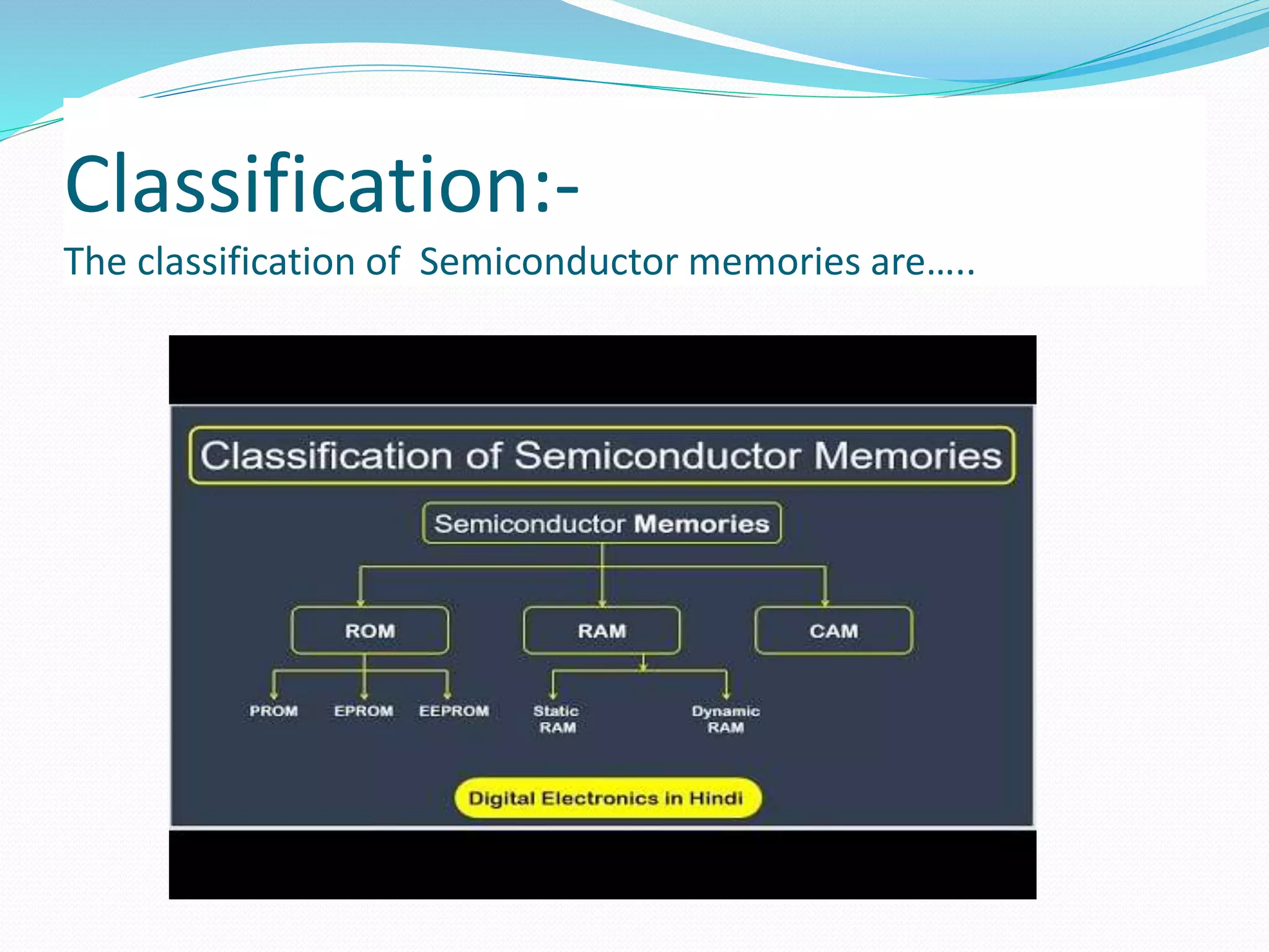
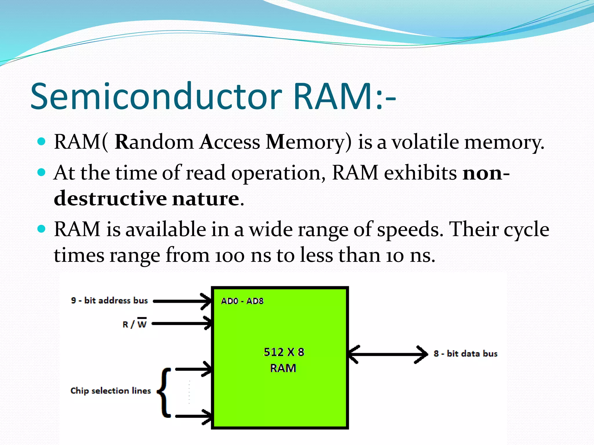
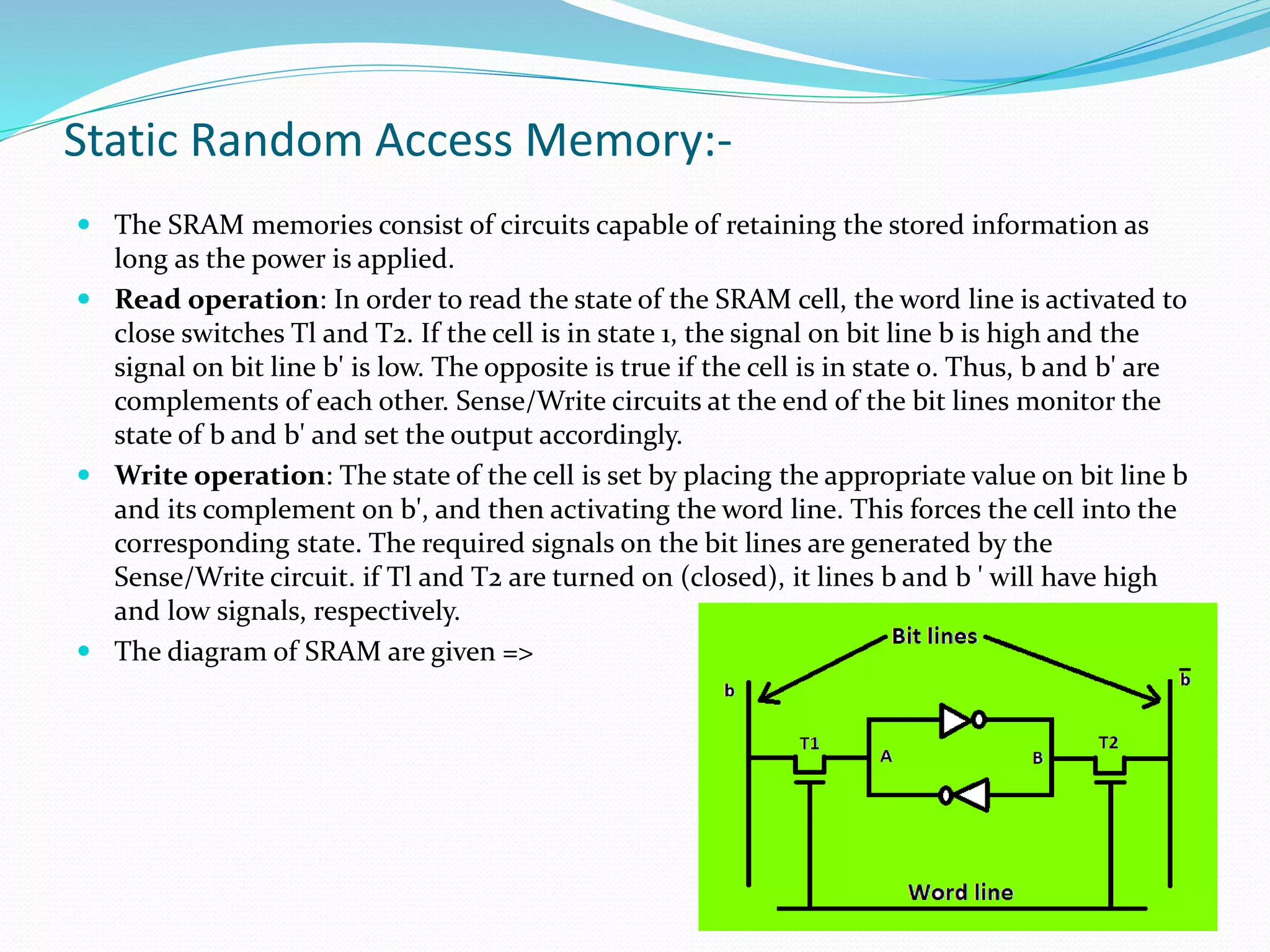
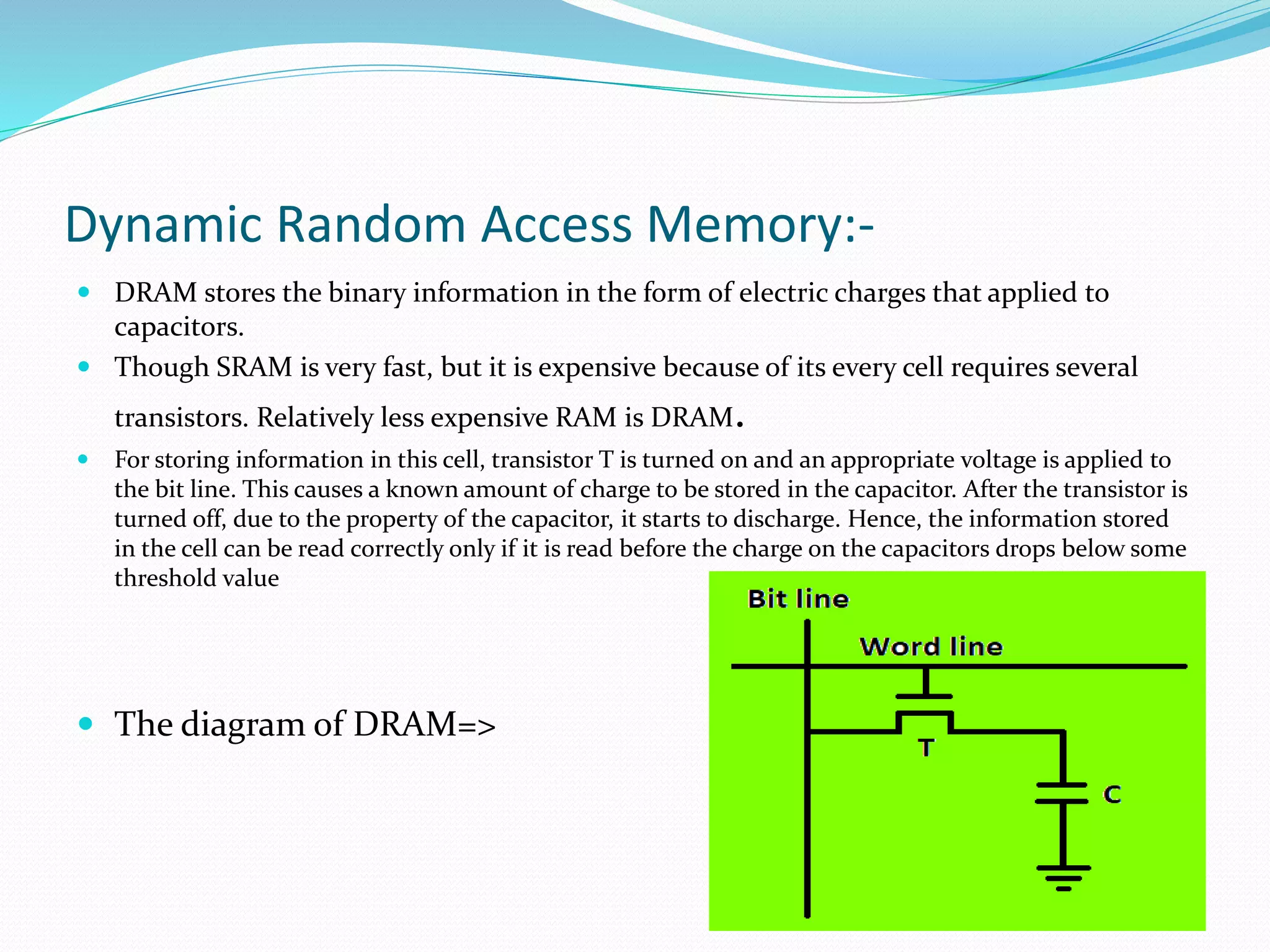
Name-Ritobeena Roy
& Muskan
Year- 3rd :
Branch-ECE :
Sem-5th
Roll- 8719210
Session- 2021-’22
Topic- SEMICONDUCTOR RAM
Semiconductor Memories:-
 Semiconductor memory is the main memory element
of a microcomputer-based system and is used to store
program and data.
 The semiconductor memory is directly accessible by
the microprocessor
 The fabrication of semiconductor memories is done
through CMOS technology.
Classification:-
The classification of Semiconductor memories are…..
Block Diagram:-
 In an IC of a semiconductor memory ,
Number of address lines=n ; Number of data lines=m.
The total memory capacity = 2n × m bits.
Memory Array:-
 The crossing points are referred to as memory cells.
 Each memory cell holds the ability to store one-bit of binary data. So,
whenever the processor sends an address to the memory IC then the row and
column decoder accordingly select one line, which correspondingly selects a
memory cell from the matrix.
Semiconductor RAM:-
 RAM( Random Access Memory) is a volatile memory.
 At the time of read operation, RAM exhibits non-
destructive nature.
 RAM is available in a wide range of speeds. Their cycle
times range from 100 ns to less than 10 ns.
INTERNAL ORGANIZATION OF RAM:-
 Read operation-The information stored in the cells selected by a word line
and transmit this information to the output data lines.
 Write operation -The Sense/Write circuits receive input information and
store it in the cells of the selected word.
Types of RAM:-
Static Random Access Memory:-
 The SRAM memories consist of circuits capable of retaining the stored information as
long as the power is applied.
 Read operation: In order to read the state of the SRAM cell, the word line is activated to
close switches Tl and T2. If the cell is in state 1, the signal on bit line b is high and the
signal on bit line b' is low. The opposite is true if the cell is in state 0. Thus, b and b' are
complements of each other. Sense/Write circuits at the end of the bit lines monitor the
state of b and b' and set the output accordingly.
 Write operation: The state of the cell is set by placing the appropriate value on bit line b
and its complement on b', and then activating the word line. This forces the cell into the
corresponding state. The required signals on the bit lines are generated by the
Sense/Write circuit. if Tl and T2 are turned on (closed), it lines b and b ' will have high
and low signals, respectively.
 The diagram of SRAM are given =>
Dynamic Random Access Memory:-
 DRAM stores the binary information in the form of electric charges that applied to
capacitors.
 Though SRAM is very fast, but it is expensive because of its every cell requires several
transistors. Relatively less expensive RAM is DRAM.
 For storing information in this cell, transistor T is turned on and an appropriate voltage is applied to
the bit line. This causes a known amount of charge to be stored in the capacitor. After the transistor is
turned off, due to the property of the capacitor, it starts to discharge. Hence, the information stored
in the cell can be read correctly only if it is read before the charge on the capacitors drops below some
threshold value
 The diagram of DRAM=>
Differences between SRAAM and DRAM:-
Thank You……

Presentation2.pptx

  • 1.
    Name-Ritobeena Roy & Muskan Year-3rd : Branch-ECE : Sem-5th Roll- 8719210 Session- 2021-’22 Topic- SEMICONDUCTOR RAM
  • 2.
    Semiconductor Memories:-  Semiconductormemory is the main memory element of a microcomputer-based system and is used to store program and data.  The semiconductor memory is directly accessible by the microprocessor  The fabrication of semiconductor memories is done through CMOS technology.
  • 3.
    Classification:- The classification ofSemiconductor memories are…..
  • 4.
    Block Diagram:-  Inan IC of a semiconductor memory , Number of address lines=n ; Number of data lines=m. The total memory capacity = 2n × m bits.
  • 5.
    Memory Array:-  Thecrossing points are referred to as memory cells.  Each memory cell holds the ability to store one-bit of binary data. So, whenever the processor sends an address to the memory IC then the row and column decoder accordingly select one line, which correspondingly selects a memory cell from the matrix.
  • 6.
    Semiconductor RAM:-  RAM(Random Access Memory) is a volatile memory.  At the time of read operation, RAM exhibits non- destructive nature.  RAM is available in a wide range of speeds. Their cycle times range from 100 ns to less than 10 ns.
  • 7.
    INTERNAL ORGANIZATION OFRAM:-  Read operation-The information stored in the cells selected by a word line and transmit this information to the output data lines.  Write operation -The Sense/Write circuits receive input information and store it in the cells of the selected word.
  • 8.
  • 9.
    Static Random AccessMemory:-  The SRAM memories consist of circuits capable of retaining the stored information as long as the power is applied.  Read operation: In order to read the state of the SRAM cell, the word line is activated to close switches Tl and T2. If the cell is in state 1, the signal on bit line b is high and the signal on bit line b' is low. The opposite is true if the cell is in state 0. Thus, b and b' are complements of each other. Sense/Write circuits at the end of the bit lines monitor the state of b and b' and set the output accordingly.  Write operation: The state of the cell is set by placing the appropriate value on bit line b and its complement on b', and then activating the word line. This forces the cell into the corresponding state. The required signals on the bit lines are generated by the Sense/Write circuit. if Tl and T2 are turned on (closed), it lines b and b ' will have high and low signals, respectively.  The diagram of SRAM are given =>
  • 10.
    Dynamic Random AccessMemory:-  DRAM stores the binary information in the form of electric charges that applied to capacitors.  Though SRAM is very fast, but it is expensive because of its every cell requires several transistors. Relatively less expensive RAM is DRAM.  For storing information in this cell, transistor T is turned on and an appropriate voltage is applied to the bit line. This causes a known amount of charge to be stored in the capacitor. After the transistor is turned off, due to the property of the capacitor, it starts to discharge. Hence, the information stored in the cell can be read correctly only if it is read before the charge on the capacitors drops below some threshold value  The diagram of DRAM=>
  • 11.
  • 12.