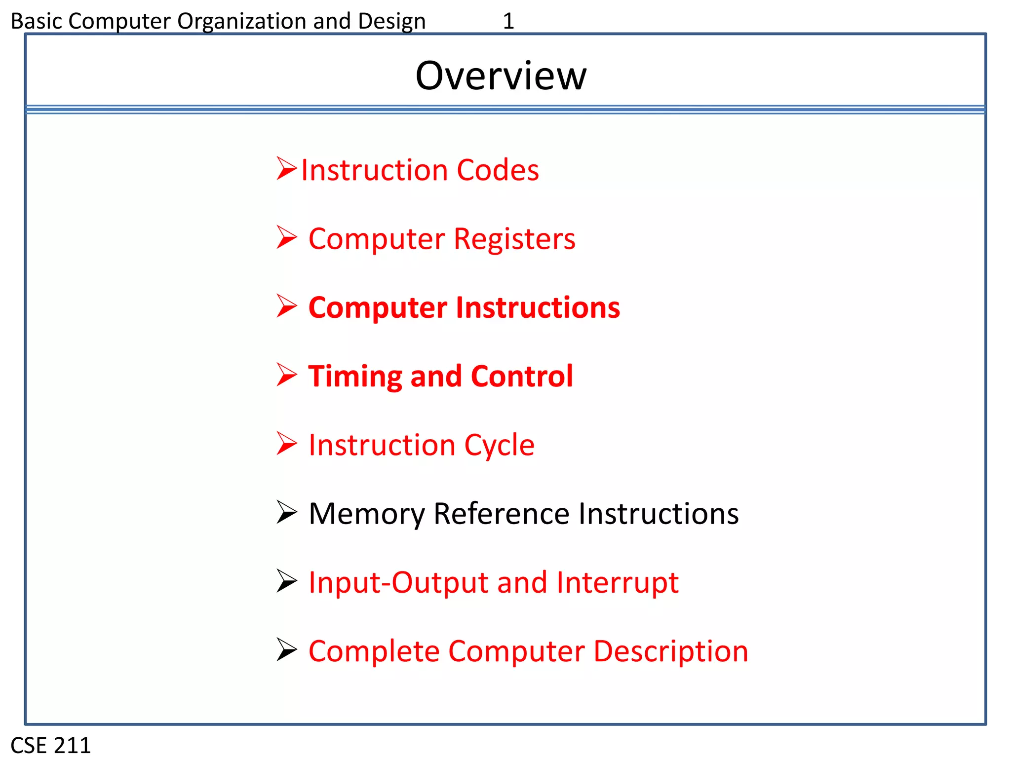
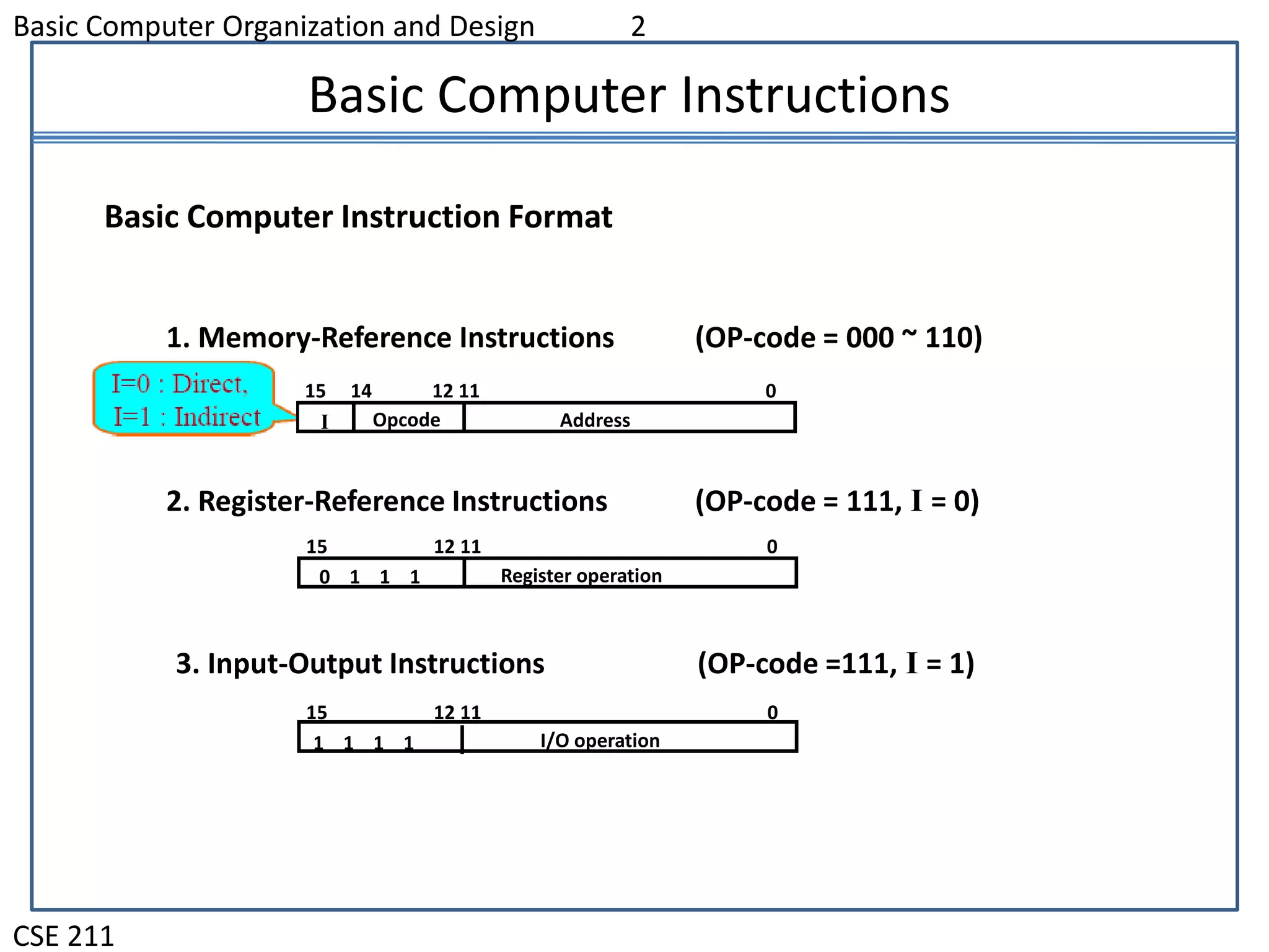
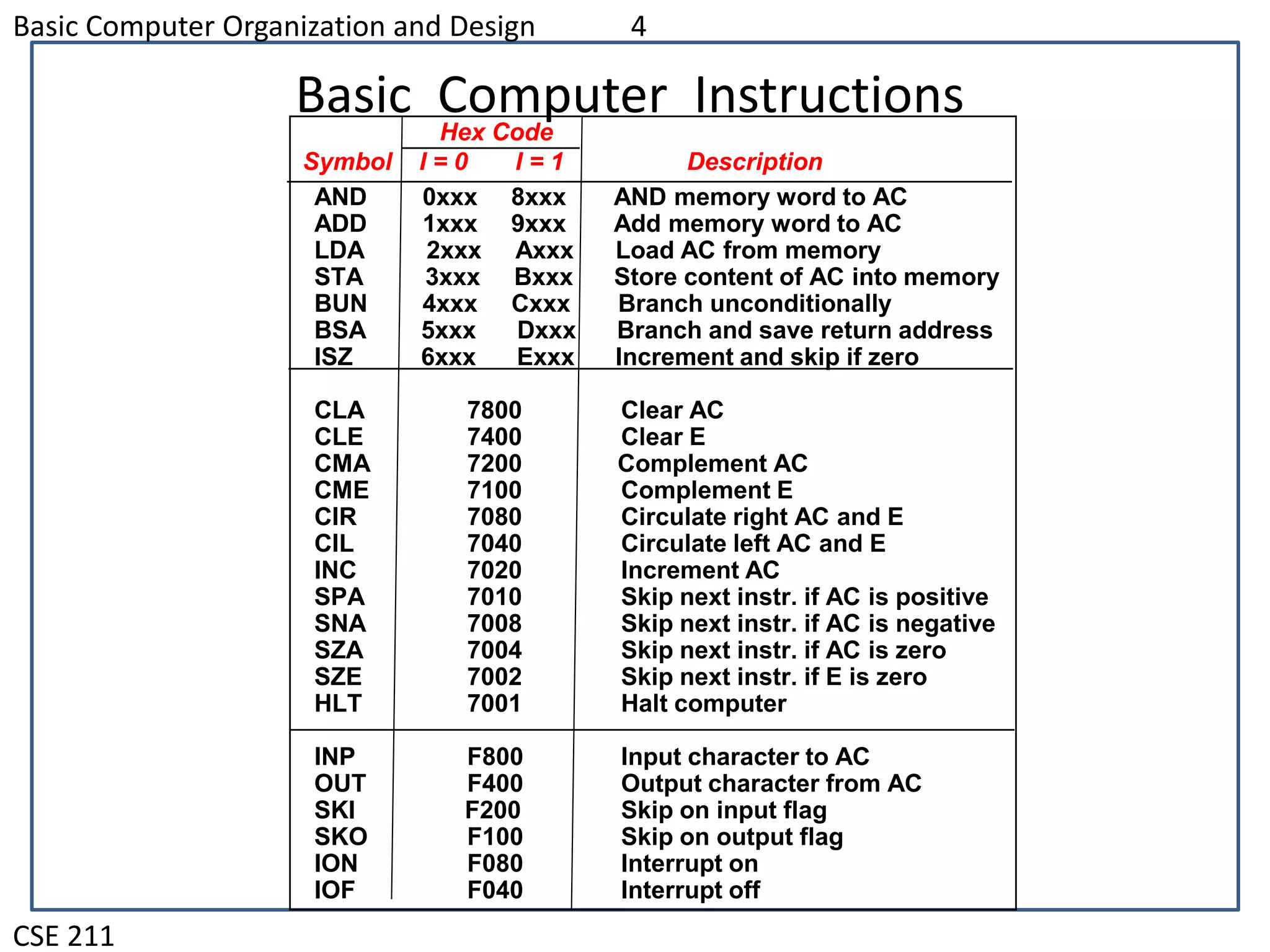
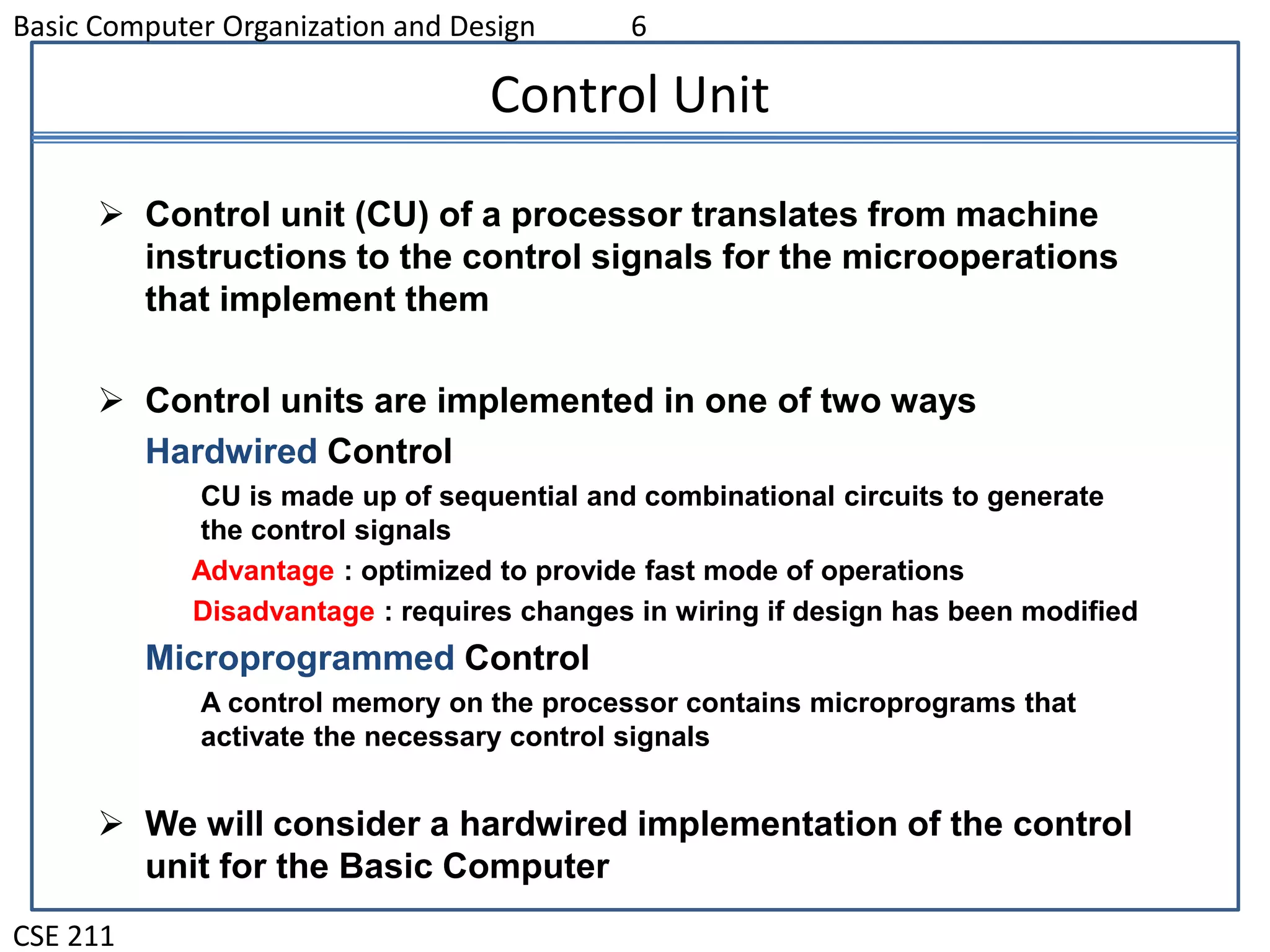
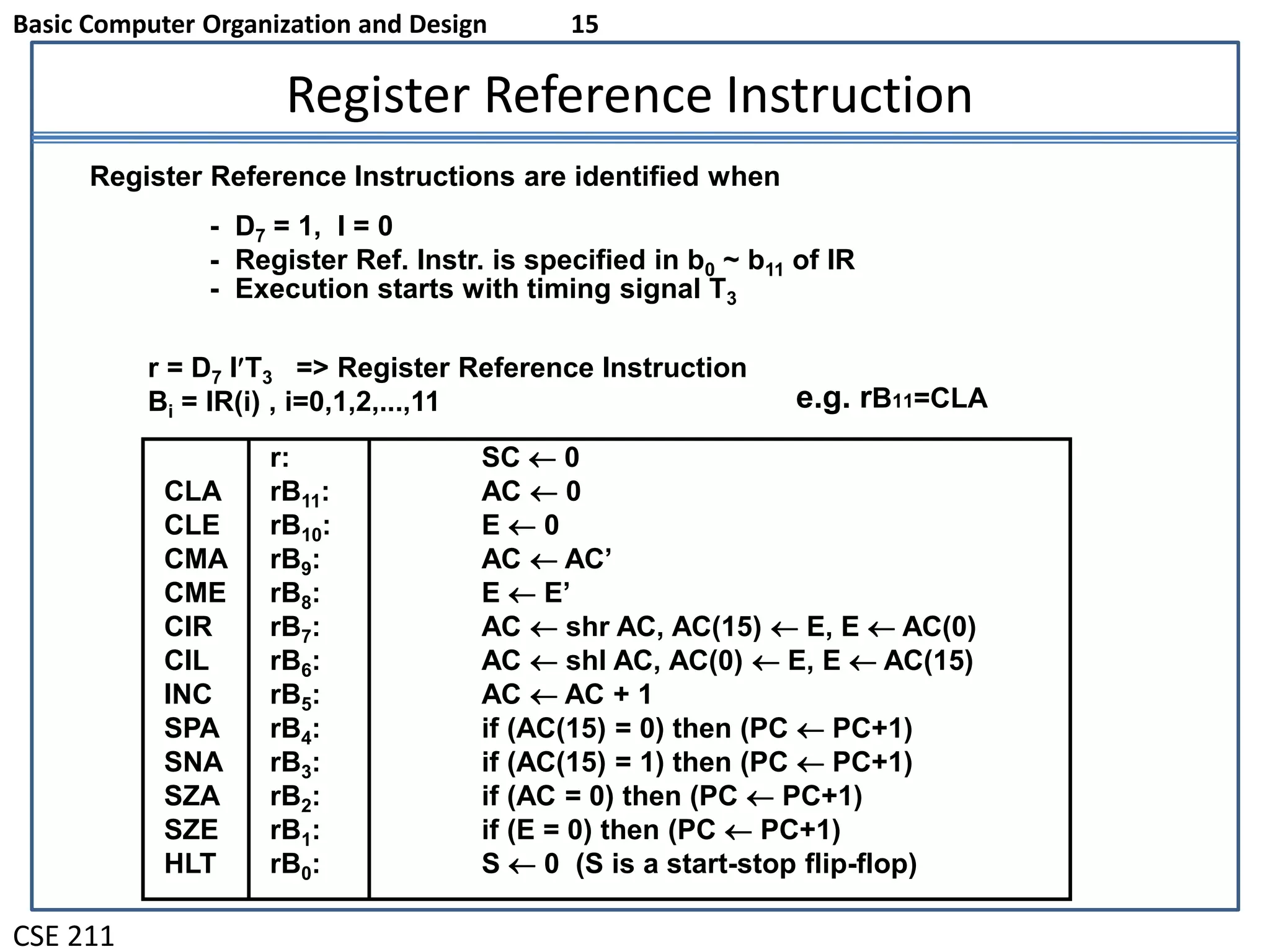
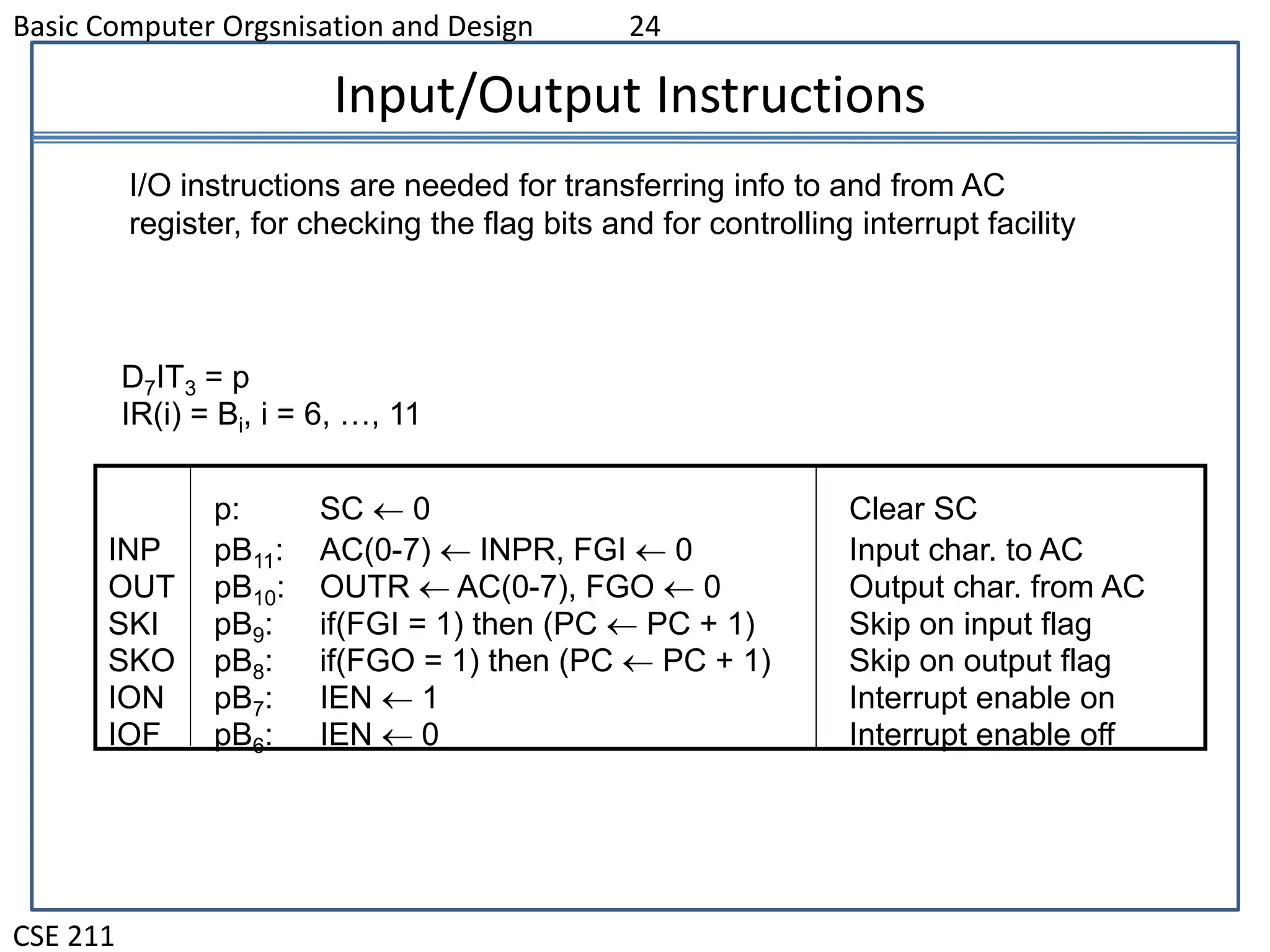
The document describes the instruction set and control unit design of a basic computer. It includes:
- Memory reference instructions like AND, ADD, LDA, STA, BUN, BSA, ISZ for arithmetic, data transfer, and control flow.
- Register reference instructions like CLA, CLE, CMA for operations using the accumulator and extended accumulator.
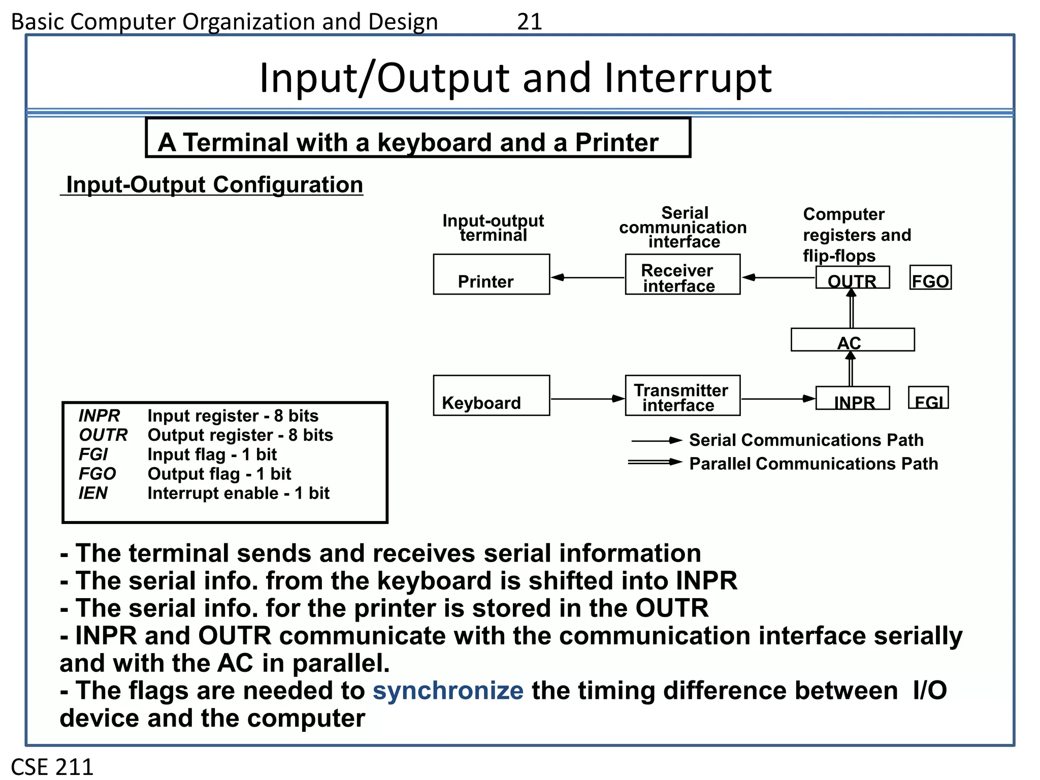
- Input/output instructions like INP, OUT for device I/O.
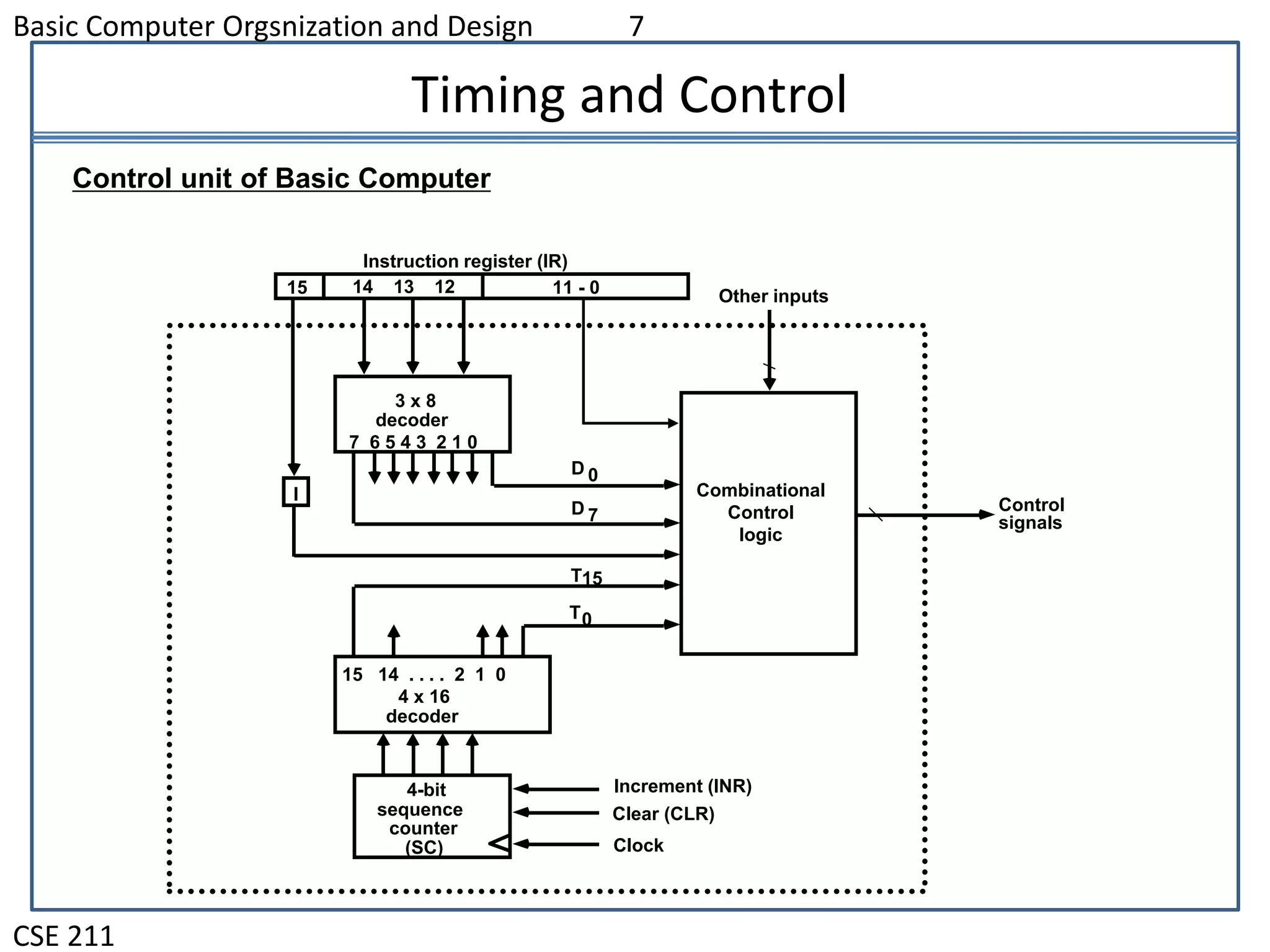
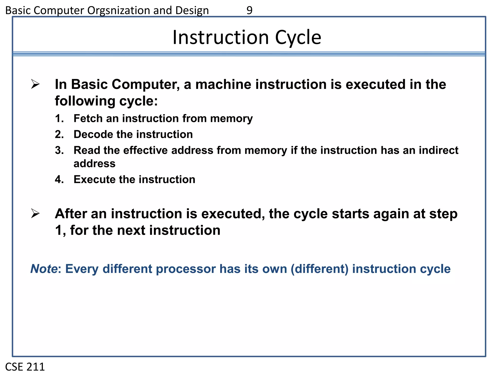
The control unit implements an instruction cycle of fetch, decode, execute through a hardwired design using a program counter, instruction register, decoders and timing signals from a sequence counter. The instruction format and timing of each instruction type is also explained.
![Basic Computer Organization and Design 10
CSE 211
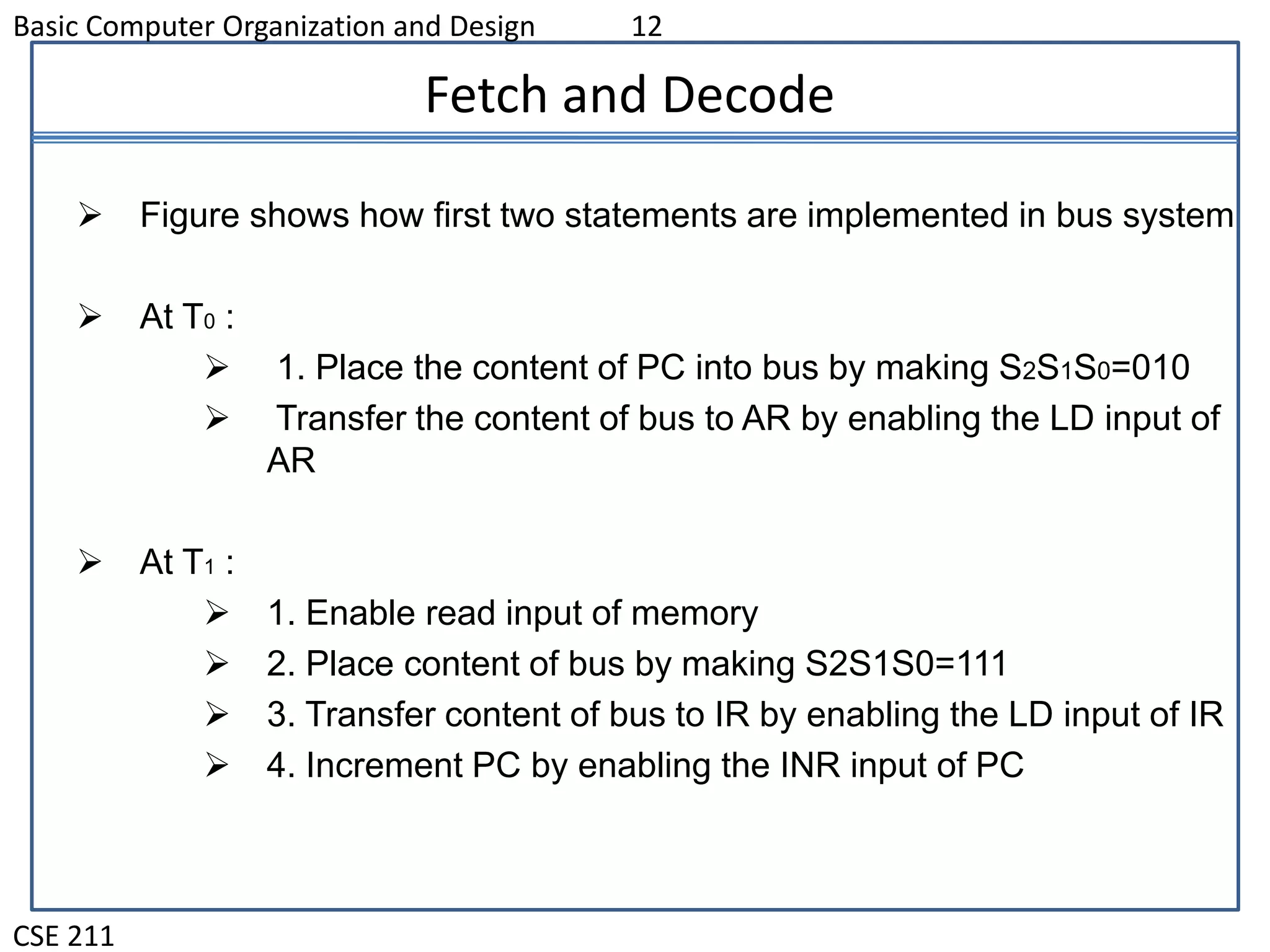
Fetch and Decode
T0: AR PC
T1: IR M [AR], PC PC + 1
T2: D0, . . . , D7 Decode IR(12-14), AR IR(0-11), I IR(15)
Initially PC loaded with address of first instruction and Sequence
counter cleared to 0, giving timing signal T0](https://image.slidesharecdn.com/chapter4-200907163811/75/Memory-Reference-instruction-10-2048.jpg)
![Basic Computer Organization and Design 11
CSE 211
Fetch and Decode
Fetch and Decode T0: AR PC (S0S1S2=010, T0=1)
T1: IR M [AR], PC PC + 1 (S0S1S2=111, T1=1)
T2: D0, . . . , D7 Decode IR(12-14), AR IR(0-11), I IR(15)
S2
S1
S0
Bus
7
Memory
unit
Address
Read
AR
LD
PC
INR
IR
LD Clock
1
2
5
Common bus
T1
T0](https://image.slidesharecdn.com/chapter4-200907163811/75/Memory-Reference-instruction-11-2048.jpg)
![Basic Computer Organization and Design 13
CSE 211
Determine the Type of Instructions
= 0 (direct)
Start
SC <-- 0
AR <-- PC
T0
IR <-- M[AR], PC <-- PC + 1
T1
AR <-- IR(0-11), I <-- IR(15)
Decode Opcode in IR(12-14),
T2
D7
= 0 (Memory-reference)(Register or I/O) = 1
II
Execute
register-reference
instruction
SC <-- 0
Execute
input-output
instruction
SC <-- 0
M[AR]<--AR Nothing
= 0 (register)(I/O) = 1 (indirect) = 1
T3 T3 T3 T3
Execute
memory-reference
instruction
SC <-- 0
T4
Fig : Flow chart for Instruction Cycle](https://image.slidesharecdn.com/chapter4-200907163811/75/Memory-Reference-instruction-13-2048.jpg)
![Basic Computer Organization and Design 14
CSE 211
Determining Type of Instruction
D'7IT3: AR M[AR]
D'7I'T3:Nothing
D7I'T3: Execute a register-reference instr.
D7IT3: Execute an input-output instr.](https://image.slidesharecdn.com/chapter4-200907163811/75/Memory-Reference-instruction-14-2048.jpg)
![Basic Computer Organization and Design 16
CSE 211
Memory Reference Instructions
AND to AC //performs AND logic with AC and memory word specified by EA
D0T4: DR M[AR] Read operand
D0T5: AC AC DR, SC 0 AND with AC
- The effective address of the instruction is in AR and was placed there during
timing signal T2 when I = 0, or during timing signal T3 when I = 1
- Memory cycle is assumed to be short enough to complete in a CPU cycle
- The execution of MR instruction starts with T4
Symbol
Operation
Decoder
Symbolic Description
AND D0 AC AC M[AR]
ADD D1 AC AC + M[AR], E Cout
LDA D2 AC M[AR]
STA D3 M[AR] AC
BUN D4 PC AR
BSA D5 M[AR] PC, PC AR + 1
ISZ D6 M[AR] M[AR] + 1, if M[AR] + 1 = 0 then PC PC+1](https://image.slidesharecdn.com/chapter4-200907163811/75/Memory-Reference-instruction-16-2048.jpg)
![Basic Computer Organization and Design 17
CSE 211
Memory Reference Instructions
ADD to AC // add content of memory word specified by EA to value of AC
sum is transferred to AC and Carry to E (Extended Accumulator)
D1T4: DR M[AR] Read operand
D1T5: AC AC + DR, E Cout, SC 0 Add to AC and store carry in E
LDA: Load to AC // Transfers memory word specified by memory address to AC
D2T4: DR M[AR]
D2T5: AC DR, SC 0
STA: Store AC // Stores the content of AC into memory specified by EA
D3T4: M[AR] AC, SC 0
BUN: Branch Unconditionally // Transfer program to instruction specified by EA
D4T4: PC AR, SC 0](https://image.slidesharecdn.com/chapter4-200907163811/75/Memory-Reference-instruction-17-2048.jpg)
![Basic Computer Organization and Design 18
CSE 211
Memory Reference Instructions
Memory, PC after execution
21
0 BSA 135
Next instruction
Subroutine
20
PC = 21
AR = 135
136
1 BUN 135
Memory, PC, AR at time T4
0 BSA 135
Next instruction
Subroutine
20
21
135
PC = 136
1 BUN 135
BSA: Branch and Save Return Address // 1. stores address of next instruction in
sequence (PC) into address specified by EA 2. EA+1 transfer to PC serve as 1st inst. In
subroutine
M[AR] PC, PC AR + 1
BSA:
D5T4: M[AR] PC, AR AR + 1
D5T5: PC AR, SC 0
BSA: Example
M[135] 21, PC 135 + 1=136](https://image.slidesharecdn.com/chapter4-200907163811/75/Memory-Reference-instruction-18-2048.jpg)
![Basic Computer Organization and Design 19
CSE 211
Memory Reference Instructions
ISZ: Increment and Skip-if-Zero
// increments the word specified by effective address,
and if incremented value=0 , PC incremented by 1
D6T4: DR M[AR]
D6T5: DR DR + 1
D6T4: M[AR] DR, if (DR = 0) then (PC PC + 1), SC 0](https://image.slidesharecdn.com/chapter4-200907163811/75/Memory-Reference-instruction-19-2048.jpg)
![Basic Computer Organization and Design 20
CSE 211
Flow Chart - Memory Reference Instructions
Memory-reference instruction
DR M[AR] DR M[AR] DR M[AR] M[AR] AC
SC 0
AND ADD LDA STA
AC AC DR
SC 0
AC AC + DR
E Cout
SC 0
AC DR
SC 0
D T0 4 D T1 4 D T2 4 D T3 4
D T0 5 D T1 5 D T2 5
PC AR
SC 0
M[AR] PC
AR AR + 1
DR M[AR]
BUN BSA ISZ
D T4 4 D T5 4 D T6 4
DR DR + 1
D T5 5 D T6 5
PC AR
SC 0
M[AR] DR
If (DR = 0)
then (PC PC + 1)
SC 0
D T6 6](https://image.slidesharecdn.com/chapter4-200907163811/75/Memory-Reference-instruction-20-2048.jpg)
![Basic Computer Organization and Design 27
CSE 211
Flow Chart of Interrupt Cycle
R = Interrupt f/f
- The interrupt cycle is a HW implementation of a branch and save return address
operation.
- At the beginning of the next instruction cycle, the instruction that is read from
memory is in address 1.
- At memory address 1, the programmer must store a branch instruction that sends
the control to an interrupt service routine
- The instruction that returns the control to the original program is "indirect BUN 0"
Store return address
R
=1=0
in location 0
M[0] PC
Branch to location 1
PC 1
IEN 0
R 0
Interrupt cycleInstruction cycle
Fetch and decode
instructions
IEN
FGI
FGO
Execute
instructions
R 1
=1
=1
=1
=0
=0
=0
INPR Input register - 8 bits
OUTR Output register - 8 bits
FGI Input flag - 1 bit
FGO Output flag - 1 bit
IEN Interrupt enable - 1 bit](https://image.slidesharecdn.com/chapter4-200907163811/75/Memory-Reference-instruction-26-2048.jpg)
![Basic Computer Orgsnization and Design 28
CSE 211
Register Transfer Operations in Interrupt Cycle
Register Transfer Statements for Interrupt Cycle
- R F/F 1 if IEN (FGI + FGO)T0T1T2
T0T1T2 (IEN)(FGI + FGO): R 1
- The fetch and decode phases of the instruction cycle
must be modified Replace T0, T1, T2 with R'T0, R'T1, R'T2
- The interrupt cycle :
RT0: AR 0, TR PC
RT1: M[AR] TR, PC 0
RT2: PC PC + 1, IEN 0, R 0, SC 0
After interrupt cycle
0 BUN 1120
0
1
PC = 256
255
1 BUN 0
Before interrupt
Main
Program
1120
I/O
Program
0 BUN 1120
0
PC = 1
256
255
1 BUN 0
Memory
Main
Program
1120
I/O
Program
256](https://image.slidesharecdn.com/chapter4-200907163811/75/Memory-Reference-instruction-27-2048.jpg)
![Basic Computer Organization and Design 29
CSE 211
Complete Computer Description
=1 (I/O) =0 (Register) =1(Indir) =0(Dir)
start
SC 0, IEN 0, R 0
R
AR PC
R’T0
IR M[AR], PC PC + 1
R’T1
AR IR(0~11), I IR(15)
D0...D7 Decode IR(12 ~ 14)
R’T2
AR 0, TR PC
RT0
M[AR] TR, PC 0
RT1
PC PC + 1, IEN 0
R 0, SC 0
RT2
D7
I I
Execute
I/O
Instruction
Execute
RR
Instruction
AR <- M[AR] Idle
D7IT3 D7I’T3 D7’IT3 D7’I’T3
Execute MR
Instruction
=0(Instruction =1(Interrupt
Cycle) Cycle)
=1(Register or I/O) =0(Memory Ref)
D7’T4
INPR Input register - 8 bits
OUTR Output register - 8 bits
FGI Input flag - 1 bit
FGO Output flag - 1 bit
IEN Interrupt enable - 1 bit](https://image.slidesharecdn.com/chapter4-200907163811/75/Memory-Reference-instruction-28-2048.jpg)
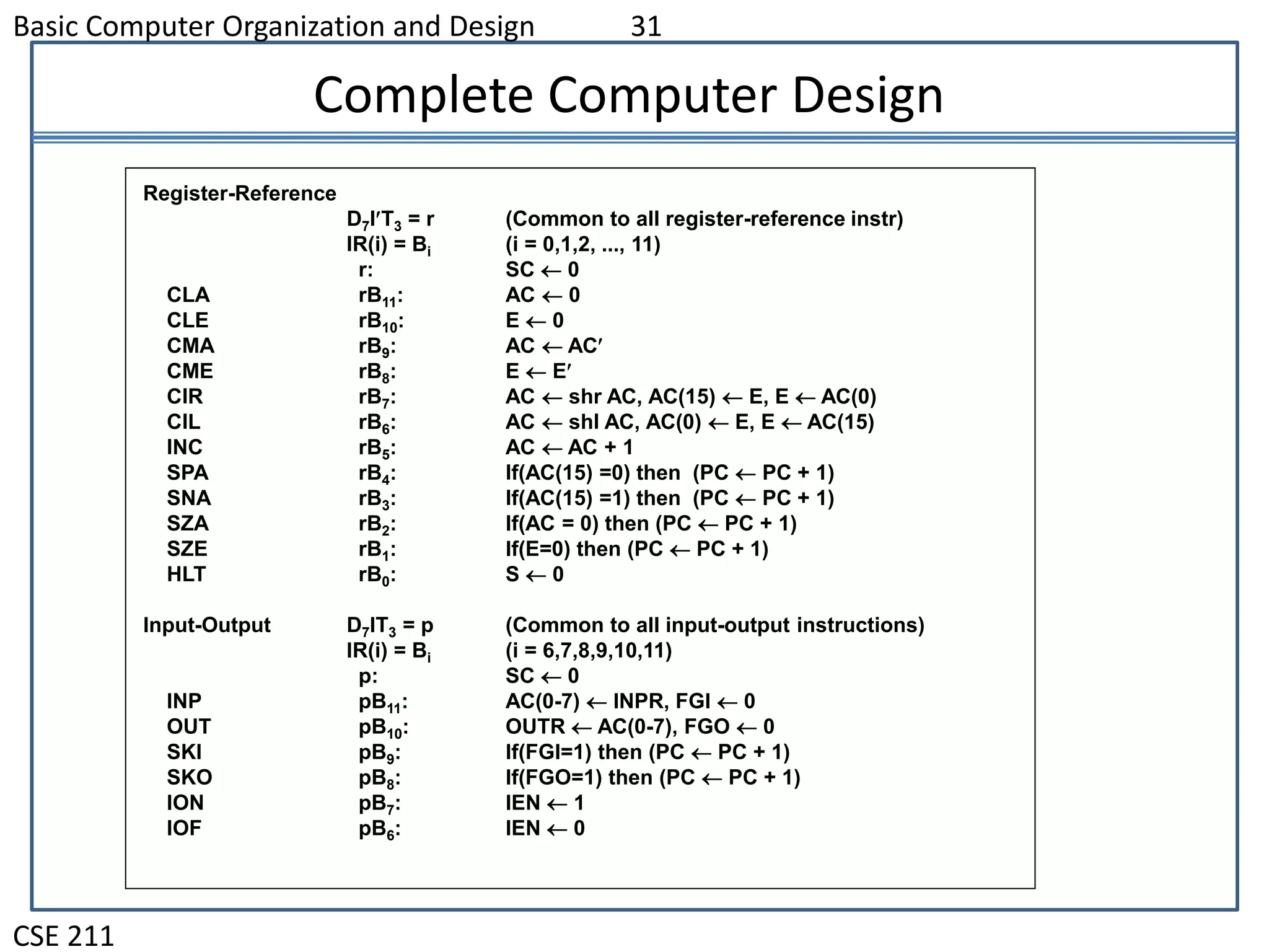
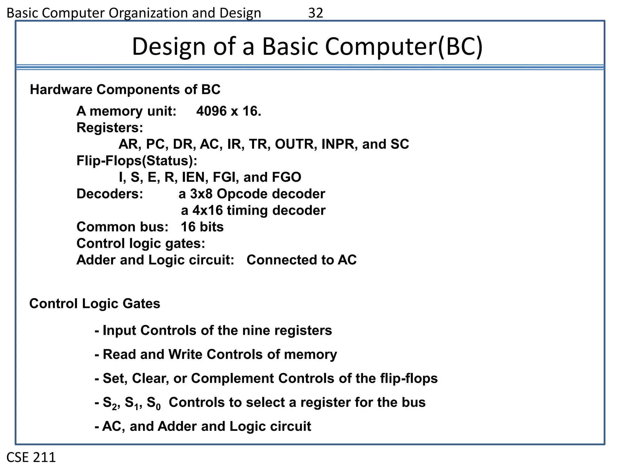
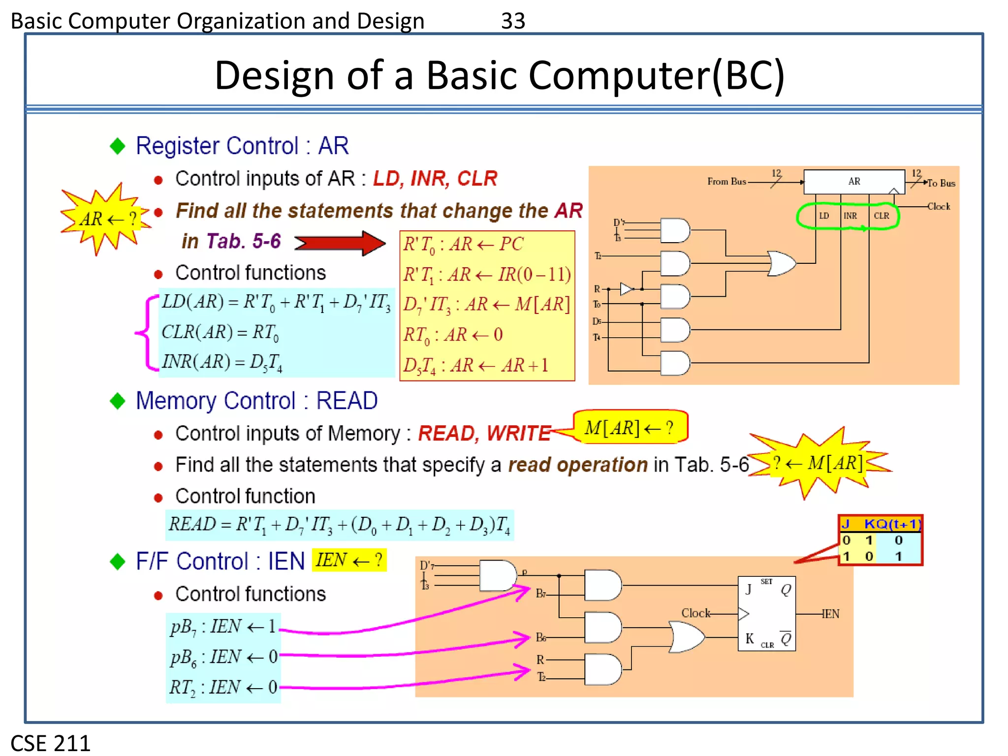
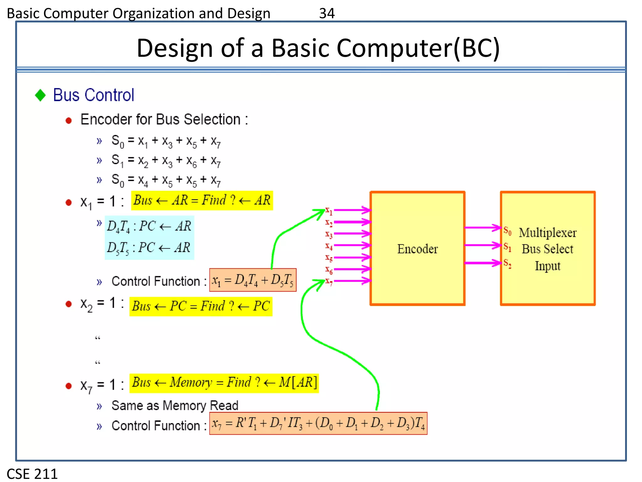
![Basic Computer Organization and Design 30
CSE 211
Complete Computer Design
Fetch
Decode
Indirect
Interrupt
Memory-Reference
AND
ADD
LDA
STA
BUN
BSA
ISZ
RT0:
RT1:
RT2:
D7IT3:
RT0:
RT1:
RT2:
D0T4:
D0T5:
D1T4:
D1T5:
D2T4:
D2T5:
D3T4:
D4T4:
D5T4:
D5T5:
D6T4:
D6T5:
D6T6:
AR PC
IR M[AR], PC PC + 1
D0, ..., D7 Decode IR(12 ~ 14),
AR IR(0 ~ 11), I IR(15)
AR M[AR]
R 1
AR 0, TR PC
M[AR] TR, PC 0
PC PC + 1, IEN 0, R 0, SC 0
DR M[AR]
AC AC DR, SC 0
DR M[AR]
AC AC + DR, E Cout, SC 0
DR M[AR]
AC DR, SC 0
M[AR] AC, SC 0
PC AR, SC 0
M[AR] PC, AR AR + 1
PC AR, SC 0
DR M[AR]
DR DR + 1
M[AR] DR, if(DR=0) then (PC PC + 1),
SC 0](https://image.slidesharecdn.com/chapter4-200907163811/75/Memory-Reference-instruction-29-2048.jpg)